JP5669606B2 - Liquid crystal display device and electronic device - Google Patents
Liquid crystal display device and electronic device Download PDFInfo
- Publication number
- JP5669606B2 JP5669606B2 JP2011024942A JP2011024942A JP5669606B2 JP 5669606 B2 JP5669606 B2 JP 5669606B2 JP 2011024942 A JP2011024942 A JP 2011024942A JP 2011024942 A JP2011024942 A JP 2011024942A JP 5669606 B2 JP5669606 B2 JP 5669606B2
- Authority
- JP
- Japan
- Prior art keywords
- liquid crystal
- image signal
- image
- display device
- crystal display
- Prior art date
- Legal status (The legal status is an assumption and is not a legal conclusion. Google has not performed a legal analysis and makes no representation as to the accuracy of the status listed.)
- Expired - Fee Related
Links
Images


Classifications
-
- G—PHYSICS
- G09—EDUCATION; CRYPTOGRAPHY; DISPLAY; ADVERTISING; SEALS
- G09G—ARRANGEMENTS OR CIRCUITS FOR CONTROL OF INDICATING DEVICES USING STATIC MEANS TO PRESENT VARIABLE INFORMATION
- G09G3/00—Control arrangements or circuits, of interest only in connection with visual indicators other than cathode-ray tubes
- G09G3/20—Control arrangements or circuits, of interest only in connection with visual indicators other than cathode-ray tubes for presentation of an assembly of a number of characters, e.g. a page, by composing the assembly by combination of individual elements arranged in a matrix no fixed position being assigned to or needed to be assigned to the individual characters or partial characters
- G09G3/34—Control arrangements or circuits, of interest only in connection with visual indicators other than cathode-ray tubes for presentation of an assembly of a number of characters, e.g. a page, by composing the assembly by combination of individual elements arranged in a matrix no fixed position being assigned to or needed to be assigned to the individual characters or partial characters by control of light from an independent source
- G09G3/36—Control arrangements or circuits, of interest only in connection with visual indicators other than cathode-ray tubes for presentation of an assembly of a number of characters, e.g. a page, by composing the assembly by combination of individual elements arranged in a matrix no fixed position being assigned to or needed to be assigned to the individual characters or partial characters by control of light from an independent source using liquid crystals
- G09G3/3611—Control of matrices with row and column drivers
- G09G3/3648—Control of matrices with row and column drivers using an active matrix
-
- G—PHYSICS
- G02—OPTICS
- G02F—OPTICAL DEVICES OR ARRANGEMENTS FOR THE CONTROL OF LIGHT BY MODIFICATION OF THE OPTICAL PROPERTIES OF THE MEDIA OF THE ELEMENTS INVOLVED THEREIN; NON-LINEAR OPTICS; FREQUENCY-CHANGING OF LIGHT; OPTICAL LOGIC ELEMENTS; OPTICAL ANALOGUE/DIGITAL CONVERTERS
- G02F1/00—Devices or arrangements for the control of the intensity, colour, phase, polarisation or direction of light arriving from an independent light source, e.g. switching, gating or modulating; Non-linear optics
- G02F1/01—Devices or arrangements for the control of the intensity, colour, phase, polarisation or direction of light arriving from an independent light source, e.g. switching, gating or modulating; Non-linear optics for the control of the intensity, phase, polarisation or colour
- G02F1/13—Devices or arrangements for the control of the intensity, colour, phase, polarisation or direction of light arriving from an independent light source, e.g. switching, gating or modulating; Non-linear optics for the control of the intensity, phase, polarisation or colour based on liquid crystals, e.g. single liquid crystal display cells
- G02F1/133—Constructional arrangements; Operation of liquid crystal cells; Circuit arrangements
- G02F1/136—Liquid crystal cells structurally associated with a semi-conducting layer or substrate, e.g. cells forming part of an integrated circuit
- G02F1/1362—Active matrix addressed cells
- G02F1/1368—Active matrix addressed cells in which the switching element is a three-electrode device
-
- G—PHYSICS
- G09—EDUCATION; CRYPTOGRAPHY; DISPLAY; ADVERTISING; SEALS
- G09G—ARRANGEMENTS OR CIRCUITS FOR CONTROL OF INDICATING DEVICES USING STATIC MEANS TO PRESENT VARIABLE INFORMATION
- G09G2300/00—Aspects of the constitution of display devices
- G09G2300/04—Structural and physical details of display devices
- G09G2300/0421—Structural details of the set of electrodes
- G09G2300/0426—Layout of electrodes and connections
-
- G—PHYSICS
- G09—EDUCATION; CRYPTOGRAPHY; DISPLAY; ADVERTISING; SEALS
- G09G—ARRANGEMENTS OR CIRCUITS FOR CONTROL OF INDICATING DEVICES USING STATIC MEANS TO PRESENT VARIABLE INFORMATION
- G09G2300/00—Aspects of the constitution of display devices
- G09G2300/08—Active matrix structure, i.e. with use of active elements, inclusive of non-linear two terminal elements, in the pixels together with light emitting or modulating elements
- G09G2300/0876—Supplementary capacities in pixels having special driving circuits and electrodes instead of being connected to common electrode or ground; Use of additional capacitively coupled compensation electrodes
-
- G—PHYSICS
- G09—EDUCATION; CRYPTOGRAPHY; DISPLAY; ADVERTISING; SEALS
- G09G—ARRANGEMENTS OR CIRCUITS FOR CONTROL OF INDICATING DEVICES USING STATIC MEANS TO PRESENT VARIABLE INFORMATION
- G09G2310/00—Command of the display device
- G09G2310/08—Details of timing specific for flat panels, other than clock recovery
-
- G—PHYSICS
- G09—EDUCATION; CRYPTOGRAPHY; DISPLAY; ADVERTISING; SEALS
- G09G—ARRANGEMENTS OR CIRCUITS FOR CONTROL OF INDICATING DEVICES USING STATIC MEANS TO PRESENT VARIABLE INFORMATION
- G09G2320/00—Control of display operating conditions
- G09G2320/02—Improving the quality of display appearance
- G09G2320/0247—Flicker reduction other than flicker reduction circuits used for single beam cathode-ray tubes
-
- G—PHYSICS
- G09—EDUCATION; CRYPTOGRAPHY; DISPLAY; ADVERTISING; SEALS
- G09G—ARRANGEMENTS OR CIRCUITS FOR CONTROL OF INDICATING DEVICES USING STATIC MEANS TO PRESENT VARIABLE INFORMATION
- G09G2330/00—Aspects of power supply; Aspects of display protection and defect management
- G09G2330/02—Details of power systems and of start or stop of display operation
- G09G2330/021—Power management, e.g. power saving
-
- G—PHYSICS
- G09—EDUCATION; CRYPTOGRAPHY; DISPLAY; ADVERTISING; SEALS
- G09G—ARRANGEMENTS OR CIRCUITS FOR CONTROL OF INDICATING DEVICES USING STATIC MEANS TO PRESENT VARIABLE INFORMATION
- G09G2340/00—Aspects of display data processing
- G09G2340/04—Changes in size, position or resolution of an image
- G09G2340/0407—Resolution change, inclusive of the use of different resolutions for different screen areas
- G09G2340/0435—Change or adaptation of the frame rate of the video stream
Landscapes
- Physics & Mathematics (AREA)
- Engineering & Computer Science (AREA)
- General Physics & Mathematics (AREA)
- Crystallography & Structural Chemistry (AREA)
- Chemical & Material Sciences (AREA)
- Theoretical Computer Science (AREA)
- Computer Hardware Design (AREA)
- Nonlinear Science (AREA)
- Microelectronics & Electronic Packaging (AREA)
- Mathematical Physics (AREA)
- Optics & Photonics (AREA)
- Control Of Indicators Other Than Cathode Ray Tubes (AREA)
- Liquid Crystal Display Device Control (AREA)
- Liquid Crystal (AREA)
- Thin Film Transistor (AREA)
Description
本発明は、液晶表示装置に関する。または、液晶表示装置の駆動方法に関する。または、液晶表示装置を具備する電子機器に関する。 The present invention relates to a liquid crystal display device. Alternatively, the present invention relates to a driving method of a liquid crystal display device. Alternatively, the present invention relates to an electronic device including a liquid crystal display device.
液晶表示装置は、テレビ受像機などの大型表示装置から携帯電話などの小型表示装置に至るまで、普及が進んでいる。今後は、より付加価値の高い製品が求められており開発が進められている。近年では、地球環境への関心の高まり、及びモバイル機器の利便性向上の点から、低消費電力型の液晶表示装置の開発が注目されている。 Liquid crystal display devices are spreading from large display devices such as television receivers to small display devices such as mobile phones. In the future, products with higher added value are required and are being developed. In recent years, attention has been focused on the development of a low power consumption type liquid crystal display device from the viewpoint of increasing interest in the global environment and improving the convenience of mobile devices.
非特許文献1では、液晶表示装置の低消費電力化を図るために、動画表示と静止画表示の際のリフレッシュレートを異ならせる構成について開示している。そして静止画表示の際の、休止期間と走査期間の信号切り替えに伴ってドレイン−コモン電圧の変動を伴い、フリッカが知覚されてしまうのを防ぐために、休止期間中にも信号線とコモン電極とに同位相の交流信号を印加してドレイン−コモン電圧の変動を防ぐ構成について開示している。
Non-Patent
上記非特許文献1のように、静止画を表示する際のリフレッシュレートを小さくすることで低消費電力化を図ることができる。しかしながら、画素トランジスタのオフ電流、及び/または液晶からの電流のリークにより画素電極の電位が変化するため、画素電極とコモン電極との間の電圧が一定に保持できないことがある。その結果、液晶に印加される電圧が変化することにより、所望の階調が得られず表示する画像が劣化してしまう問題がある。
As in
多階調の表示を行う際には階調の変化が生じやすいため、階調が変化しない程度にリフレッシュレートを保つ必要がある。その結果、リフレッシュレートを小さくすることによる液晶表示装置の低消費電力化を十分に図ることができないといった問題がある。 When multi-gradation display is performed, a change in gradation is likely to occur. Therefore, it is necessary to maintain the refresh rate to such an extent that the gradation does not change. As a result, there is a problem that the power consumption of the liquid crystal display device cannot be sufficiently reduced by reducing the refresh rate.
そこで、本発明の一態様は、リフレッシュレートを低減して静止画を表示する際の、階調が変化することによる画質の劣化を抑制することを課題の一とする。 In view of the above, an object of one embodiment of the present invention is to suppress deterioration in image quality due to a change in gradation when a still image is displayed at a reduced refresh rate.
本発明の一態様は、駆動回路によって制御される表示部と、駆動回路を制御するためのタイミングコントローラと、を有し、タイミングコントローラには、静止画を表示するための画像信号が供給されており、タイミングコントローラにより、画像信号の階調数が小さいほど、表示部において画像信号に応じた画像を表示する際のリフレッシュレートを小さくする液晶表示装置である。 One embodiment of the present invention includes a display portion controlled by a drive circuit and a timing controller for controlling the drive circuit, and the timing controller is supplied with an image signal for displaying a still image. In the liquid crystal display device, the refresh rate when the image corresponding to the image signal is displayed on the display unit is decreased as the number of gradations of the image signal is decreased by the timing controller.
本発明の一態様は、駆動回路によって制御される表示部と、駆動回路を制御するためのタイミングコントローラと、を有し、タイミングコントローラにより、表示部で静止画を表示するための第1の階調数の第1の画像信号に応じた画像を表示する際のリフレッシュレートよりも、第1の階調数より小さい第2の階調数の第2の画像信号に応じた画像を表示する際のリフレッシュレートを小さくする液晶表示装置である。 One embodiment of the present invention includes a display portion controlled by a drive circuit, and a timing controller for controlling the drive circuit, and a first floor for displaying a still image on the display portion by the timing controller. When displaying an image according to a second image signal having a second gradation number smaller than the first gradation number than a refresh rate when displaying an image according to the first image signal having a logarithm. This is a liquid crystal display device that reduces the refresh rate.
本発明の一態様において、タイミングコントローラは、画像信号の階調数を判定するための分析部と、分析部からの信号をもとにリフレッシュレートを記憶するルックアップテーブル部と、ルックアップテーブル部により制御されるパネルコントローラと、を有する液晶表示装置でもよい。 In one embodiment of the present invention, a timing controller includes an analysis unit for determining the number of gradations of an image signal, a lookup table unit that stores a refresh rate based on a signal from the analysis unit, and a lookup table unit And a liquid crystal display device having a panel controller controlled by the control unit.
本発明の一態様において、分析部は、画像信号のビット毎に設けられたカウンタ回路と、カウンタ回路でのカウント値をもとに階調値を判定する判定部と、を有する液晶表示装置でもよい。 In one embodiment of the present invention, the analysis unit may be a liquid crystal display device including a counter circuit provided for each bit of the image signal and a determination unit that determines a gradation value based on a count value in the counter circuit. Good.
本発明の一態様において、表示部の各画素は、画像信号の書き込みを制御するためのトランジスタを有し、トランジスタの半導体層は酸化物半導体である液晶表示装置でもよい。 In one embodiment of the present invention, each pixel of the display portion may include a transistor for controlling writing of an image signal, and the semiconductor layer of the transistor may be a liquid crystal display device that is an oxide semiconductor.
本発明の一態様により、リフレッシュレートを低減して静止画を表示する際の、階調が変化することによる画質の劣化を小さくすることができる。また、静止画を表示する際にリフレッシュレートを小さくすることで、低消費電力化を図ることができる。 According to one embodiment of the present invention, when a still image is displayed with a reduced refresh rate, deterioration in image quality due to change in gradation can be reduced. In addition, the power consumption can be reduced by reducing the refresh rate when displaying a still image.
以下、本発明の実施の形態について図面を参照しながら説明する。但し、本発明は多くの異なる態様で実施することが可能であり、本発明の趣旨及びその範囲から逸脱することなくその形態及び詳細を様々に変更し得ることは当業者であれば容易に理解される。従って実施の形態の記載内容に限定して解釈されるものではない。なお、以下に説明する本発明の構成において、同じ物を指し示す符号は異なる図面間において共通とする。 Hereinafter, embodiments of the present invention will be described with reference to the drawings. However, the present invention can be implemented in many different modes, and those skilled in the art can easily understand that the modes and details can be variously changed without departing from the spirit and scope of the present invention. Is done. Therefore, the present invention is not construed as being limited to the description of the embodiments. Note that in the structures of the present invention described below, the same reference numeral is used in different drawings.
なお、各実施の形態の図面等において示す各構成の、大きさ、層の厚さ、信号波形、又は領域は、明瞭化のために誇張されて表記している場合がある。よって、必ずしもそのスケールに限定されない。 Note that the size, layer thickness, signal waveform, or region of each structure illustrated in drawings and the like in the embodiments is exaggerated for simplicity in some cases. Therefore, it is not necessarily limited to the scale.
なお本明細書にて用いる第1、第2、第3、乃至第N(Nは自然数)という用語は、構成要素の混同を避けるために付したものであり、数的に限定するものではないことを付記する。 Note that the terms “first”, “second”, “third” to “N” (N is a natural number) used in this specification are given to avoid confusion of components and are not limited numerically. I will add that.
(実施の形態1)
本実施の形態では、液晶表示装置について説明するための概念図、液晶表示装置のブロック図、及び液晶素子の特性と階調数の関係図について示し、説明する。
(Embodiment 1)
In this embodiment, a conceptual diagram for describing a liquid crystal display device, a block diagram of the liquid crystal display device, and a relationship diagram between characteristics of a liquid crystal element and the number of gradation levels are shown and described.
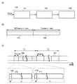
まず図1(A)乃至(C)では、液晶表示装置について説明するための概念図、及び液晶表示装置の簡単なブロック図を示し、本明細書に係る液晶表示装置について説明する。 First, in FIGS. 1A to 1C, a conceptual diagram for describing a liquid crystal display device and a simple block diagram of the liquid crystal display device are shown, and the liquid crystal display device according to this specification will be described.
図1(A)で示す液晶表示装置100は、タイミングコントローラ101(タイミング制御回路ともいう)、駆動回路102、表示部103を有する。タイミングコントローラ101には、外部より画像信号Dataが供給される。
A liquid
図1(A)で示すタイミングコントローラ101は、画像信号Dataの階調数(画像信号Dataにより表示される画像の階調数のことをいう)に応じてリフレッシュレートを変換するための機能を有する。より具体的には、表示部が有する画素に書き込んだ画像信号の保持期間を変換するための機能を有する。
The
図1(A)で示す駆動回路102は、ゲート線駆動回路(走査線駆動回路ともいう)、ソース線駆動回路(信号線駆動回路ともいう)を有する。ゲート線駆動回路、ソース線駆動回路は、複数の画素を有する表示部103を駆動するための駆動回路であり、シフトレジスタ回路(シフトレジスタともいう)又はデコーダ回路を有する。なお、ゲート線駆動回路、及びソース線駆動回路は、表示部103と同じ基板に形成されるものでもよいし、別の基板に形成されるものであってもよい。
A
図1(A)で示す表示部103は、複数の画素と、複数の画素を走査して選択するためのゲート線(走査線ともいう)と、複数の画素に画像信号を供給するためのソース線(信号線ともいう)を有する。ゲート線はゲート線駆動回路によって制御され、ソース線はソース線駆動回路によって制御される。画素はスイッチング素子としてトランジスタ、容量素子、及び液晶素子を有する。
A
本実施の形態で示す液晶表示装置100は、図1(B)に示すように動画表示期間104、及び静止画表示期間105を有する。なお本実施の形態で述べる構成では、特に静止画表示期間105での各フレーム期間における画像信号の書き込み期間、及び保持期間について説明するものである。
A liquid
なお動画表示期間104は、1フレーム期間の周期(またはフレーム周波数)が、1/60秒以下(60Hz以上)であることが望ましい。フレーム周波数を高くすることで、画像をみる人がちらつき(フリッカ)を感じないようにすることができる。また静止画表示期間105は、1フレーム期間の周期を極端に長く、例えば1分以上(0.017Hz以下)とすることが望ましい。フレーム周波数を低くすることで、複数回にわたって同じ画像を切り替える場合と比較して眼の疲労を低減するといったことも可能である。なお、フレーム周波数はリフレッシュレートのことであり、1秒間あたりの画面表示の繰り返しの回数のことである。
In the moving
なお動画表示期間104と静止画表示期間105との切り替えは、外部から切り替えるための信号を供給する構成でもよいし、画像信号Dataをもとに動画表示期間104または静止画表示期間105を判定する構成としてもよい。なお、画像信号Dataをもとに動画表示期間104と静止画表示期間105との切り替えを判定することにより切り替える場合には、図1(A)で示すタイミングコントローラ101によって、表示部103の各画素に書き込まれる画像信号が前の期間に書き込んだ画像信号と異なる画像信号である場合に逐次画像信号を書き込んで動画を表示させる動画表示期間と、表示部103の各画素に書き込まれる画像信号が前の期間に書き込んだ画像信号と同じ場合に当該画像信号の書き込みを停止し書き込まれた当該画像信号を各画素において保持して静止画を表示する静止画表示期間と、を切り替える構成とすればよい。
The switching between the moving
次いで図1(A)で示すタイミングコントローラ101の動作について説明するため、具体的な画像信号Dataとして複数の画像信号、ここでは第1の画像信号及び第2の画像信号を示し、図1(C)に示す概念図にて説明する。なお図1(C)において、第1の画像信号は第1の階調数(具体的にはM階調:Mは自然数)の画像信号であり、期間T1は第1の階調数で表示が行われる期間を示し、第2の画像信号は第2の階調数(具体的にはN階調:Nは自然数)の画像信号であり、期間T2は第2の階調数で表示が行われる期間を示す。なお第1の階調数Mは第2の階調数Nより大きい、すなわち第1の画像信号は第2の画像信号より多くの階調により画像を表示するものである。図1(C)での期間T1において示す1フレーム期間となる期間106は第1の画像信号による1フレーム期間について表したものである。図1(C)での期間T2において示す1フレーム期間となる期間107は第2の画像信号による1フレーム期間について表したものである。なお第1の階調数Mは、第2の階調数Nより大きい(M>N)ものとして以下説明するものである。
Next, in order to describe the operation of the
なお階調数は、画像を構成する画素での色の濃淡を表す際の区切りの数のことをいい、画素に書き込まれる画像信号の電圧の高低(以下、電圧レベル)によって表されるものである。具体的にいえば、液晶素子に電圧を印加することで表現される白色から黒色への変化を表す、電圧レベルの勾配を複数段に分割して得られる電圧レベルの総数である。または階調数とは、液晶素子に電圧を印加することで表現される白色から黒色への変化を表す、電圧レベルの勾配を複数段に分割して得られる電圧レベルによって表されるもののうち、実際に1フレーム期間に画像を構成する画素に供給された電圧レベルの数のことをいう。具体的には、画像を構成する画素に供給された電圧レベルの数が、そのまま階調数として表されるものである。なお複数の画像信号とは、階調数の異なる画像信号、例えば上述の第1の画像信号及び第2の画像信号のように、互いに異なる階調数の画像信号が複数供給されるものをいう。 The number of gradations refers to the number of divisions when expressing the color density of the pixels constituting the image, and is represented by the level of the voltage of the image signal written to the pixels (hereinafter referred to as voltage level). is there. Specifically, it is the total number of voltage levels obtained by dividing the voltage level gradient into a plurality of stages, which represents a change from white to black expressed by applying a voltage to the liquid crystal element. Or, the number of gradations represents a change from white to black expressed by applying a voltage to the liquid crystal element, among those expressed by the voltage level obtained by dividing the gradient of the voltage level into a plurality of stages, It means the number of voltage levels actually supplied to the pixels constituting the image in one frame period. Specifically, the number of voltage levels supplied to the pixels constituting the image is directly expressed as the number of gradations. Note that the plurality of image signals refers to an image signal having a different number of gradations, for example, a plurality of image signals having different numbers of gradations, such as the first image signal and the second image signal described above. .
本実施の形態で述べる構成では、特に静止画表示期間での画像信号により表示される画像の階調数に応じてリフレッシュレートを変換、換言すれば1フレーム期間の長さを変換する構成である。図1(C)に示すように異なる階調数の画像信号に応じてリフレッシュレートを変換、即ち期間106と期間107の長さを異ならせる。具体的には、第2の階調数Nの画像信号である期間107は、第1の階調数Mの画像信号である期間106より長く設定、即ち第1の階調数Mの画像信号によるリフレッシュレートを第2の階調数Nの画像信号によるリフレッシュレートより小さくするよう動作させる。また、リフレッシュレートをちいさくすることは、1フレーム期間長さを小さくすることに相当する。なお図1(C)では、期間106は第1の画像信号を画素に書き込む期間108(図中「W」で表記)、及び第1の画像信号を画素に保持する期間109(図中「H」で表記)を有する。期間107は第2の画像信号を画素に書き込む期間110(図中「W」で表記)、及び第2の画像信号を画素に保持する期間111(図中「H」で表記)を有する。ここで期間106と期間107の長さを異ならせるということは、第1の画像信号を画素に保持する期間109と、第2の画像信号を画素に保持する期間111との長さを異ならせるということに相当する。期間106と期間107の長さを、第1の階調数M及び第2の階調数Nに応じて変換することでリフレッシュレートを低減して静止画を表示する際の、階調が変化することによる画質の劣化を低減することができる。そして、静止画を表示する際にリフレッシュレートを小さくすることで、画像信号の書き込み頻度を低減でき、低消費電力化を図ることができる。また、同一の画像を複数回書き換えて静止画を表示する場合、画像の切り替わりが視認できると、人間は目に疲労を感じることもあり得る。そのためリフレッシュレートを大幅に小さくすることで、目の疲労を減らすといった効果もある。
In the configuration described in this embodiment, the refresh rate is converted according to the number of gradations of the image displayed by the image signal in the still image display period, in other words, the length of one frame period is converted. . As shown in FIG. 1C, the refresh rate is converted in accordance with the image signals having different gradation numbers, that is, the lengths of the
次いで本実施の形態の構成による効果について説明するため、一例として図1(C)で説明した第1の階調数M、第2の階調数Nに応じた画像信号の電圧と、液晶素子の透過率の関係について図2(A)、(B)に示す。なお図2(A)、(B)では、一例として、液晶素子に0[V]を印加する際に透過率が高い、所謂ノーマリーホワイトの液晶素子の透過率について示している。なお本実施の形態の構成は、ノーマリーブラックの液晶素子であっても同様の効果を奏するものである。また液晶素子を駆動する際には、液晶素子に印加する電圧の反転または非反転を選択する様々な反転駆動と組み合わせることができる。なお本実施の形態においては、電圧と透過率との関係は、正の極性の場合のみを示しているが、負の極性でも同様である。 Next, in order to describe the effect of the structure of this embodiment mode, as an example, the voltage of the image signal corresponding to the first number of gradations M and the second number of gradations N described in FIG. FIG. 2A and FIG. 2B show the relationship of transmittance. 2A and 2B show, as an example, the transmittance of a so-called normally white liquid crystal element that has a high transmittance when 0 [V] is applied to the liquid crystal element. Note that the configuration of this embodiment has the same effect even with a normally black liquid crystal element. Further, when driving the liquid crystal element, it can be combined with various inversion driving for selecting inversion or non-inversion of the voltage applied to the liquid crystal element. In the present embodiment, the relationship between the voltage and the transmittance is shown only in the case of positive polarity, but the same applies to the case of negative polarity.
図2(A)は、画像信号が第1の階調数Mでの電圧と透過率との関係を示している。そして図2(B)は、画像信号が第2の階調数Nでの電圧と透過率との関係を示している。 FIG. 2A shows the relationship between the voltage and transmittance of the image signal at the first number of gradations M. FIG. FIG. 2B shows the relationship between the voltage and transmittance of the image signal at the second gradation number N.
図2(A)では第1の階調数Mのうち、電圧V1が1階調201(黒)に相当し、電圧V2が2階調202(中間調)に相当し、電圧V3が3階調203(中間調)に相当し、電圧V4が4階調204(中間調)に相当し、電圧VMがM階調205(白)に相当するものとして示している。図2(B)では第2の階調数Nのうち、電圧V1が1階調211(黒)に相当し、電圧V2が2階調212(中間調)に相当し、電圧VNがN階調213(白)に相当するものとして示している。なお前述の電圧が液晶素子の両端の電極に印加される電圧である。図2(A)及び図2(B)に示すように、第1の階調数M及び第2の階調数Nとでは画像信号の階調数が少ない第2の階調数Nの方が階調間の電圧の間隔(差)が大きくなる。そのため、画素に書き込まれた画像信号の電圧が時間と共に変化しても、画像信号の階調数が小さいほど、階調の変化は少なくなる。 In FIG. 2A, among the first number of gradations M, the voltage V1 corresponds to one gradation 201 (black), the voltage V2 corresponds to two gradations 202 (halftone), and the voltage V3 is the third floor. It corresponds to the tone 203 (halftone), the voltage V4 corresponds to the four gradations 204 (halftone), and the voltage VM corresponds to the M gradation 205 (white). In FIG. 2B, out of the second gradation number N, the voltage V1 corresponds to one gradation 211 (black), the voltage V2 corresponds to two gradations 212 (halftone), and the voltage VN is Nth order. It is shown as corresponding to the key 213 (white). The aforementioned voltage is a voltage applied to the electrodes at both ends of the liquid crystal element. As shown in FIGS. 2A and 2B, the first gradation number M and the second gradation number N have a smaller gradation number of the image signal, and the second gradation number N is smaller. However, the voltage interval (difference) between gradations increases. For this reason, even if the voltage of the image signal written to the pixel changes with time, the change in gradation decreases as the number of gradations in the image signal decreases.
図3(A)及び図3(B)では、図2(A)及び図2(B)で示した電圧と透過率との関係について、さらに具体的に説明する。図3(A)は、図2(A)で示した中間調のi(iは1乃至M階調のいずれか一)階調目の前後に注目した電圧と透過率との関係を示す。図3(B)は、図2(B)で示した中間調のj(jは1乃至N階調のいずれか一)階調目の前後に注目した電圧と透過率との関係を示す。例えば図3(A)において、画像信号が第1の階調数Mの場合、電圧Viがi階調303(中間調)に相当し、電圧Vi+1が(i+1)階調304(中間調)に相当し、電圧Vi+2が(i+2)階調305(中間調)に相当し、電圧Vi−1が(i―1)階調302(中間調)に相当し、電圧Vi−2が(i−2)階調301(中間調)に相当にするものとして示している。図3(B)において、画像信号が第2の階調数Nの場合、電圧Vjがj階調312(中間調)に相当し、電圧Vj+1が(j+1)階調313(中間調)に相当し、電圧Vj−1が(j−1)階調311(中間調)に相当するものとして示している。 3A and 3B, the relationship between the voltage and the transmittance shown in FIGS. 2A and 2B will be described more specifically. FIG. 3A shows the relationship between the transmissivity and the voltage noted before and after the halftone i (i is one of 1 to M gradations) shown in FIG. 2A. FIG. 3B shows the relationship between the transmissivity and the voltage noticed before and after the halftone j (j is one of 1 to N gradations) shown in FIG. 2B. For example, in FIG. 3A, when the image signal has the first gradation number M, the voltage V i corresponds to the i gradation 303 (halftone), and the voltage V i + 1 corresponds to the (i + 1) gradation 304 (halftone). ), The voltage V i + 2 corresponds to the (i + 2) gradation 305 (halftone), the voltage V i-1 corresponds to the (i-1) gradation 302 (halftone), and the voltage V i-2. Is shown as equivalent to (i-2) gradation 301 (halftone). In FIG. 3B, when the image signal has the second gradation number N, the voltage V j corresponds to the j gradation 312 (halftone), and the voltage V j + 1 corresponds to the (j + 1) gradation 313 (halftone). The voltage V j−1 is shown as corresponding to (j−1) gradation 311 (halftone).
図3(A)において、i階調303とするために液晶素子に電圧Viを印加する。また図3(B)において、j階調312とするために液晶素子に電圧Vjを印加する。そして電圧Vi、電圧Vjを印加した後、時間の経過と共に、液晶素子に印加する電圧がα(αは正の数)だけ減少し、電圧Vi−α、電圧Vj−αとなるとする。図3(A)において電圧Vi−αとなった電圧値は、(i+1)階調304(中間調)と(i+2)階調305との間の階調306に減少すること(図3(A))中、矢印307参照)となり、電圧の減少により(i+1)階調304(中間調)または(i+2)階調の階調として視認されることとなる。また図3(B)において電圧Vj−αとなった電圧値は、j階調312(中間調)と(j+1)階調313との間の階調314に減少すること(図3(B))中、矢印315参照)となり、電圧の減少によりj階調312(中間調)または(j+1)階調313の階調として視認されることとなる。図3(A)、図3(B)から、液晶素子に印加される電圧Vi、電圧Vjは、同じ電圧αだけ減少したにも係わらず、画像信号が第1の階調数Mの場合(図3(A))よりも、画像信号が第2の階調数Nの場合(図3(B))のほうが、電圧の変化による階調の変化が小さいことが分かる。つまり、階調数の大きい第1の階調数Mによる画像信号よりも、階調数の小さい第2の階調数Nの画像信号の方が、画素に書き込んだ画像信号を保持したまま同じ期間が経過することによる電圧の減少が生じる際に、階調の変化による画質の劣化を小さくすることができる。そのため、階調数の小さい第2の階調数Nの画像信号に応じた画像を表示する際には、階調数の大きい第1の階調数Mによる画像信号に応じた画像を表示する場合に比べて、リフレッシュレートを小さくしても静止画を表示する際の、階調が変化することによる画質の劣化を小さくすることができる。そして階調数の小さい第2の階調数Nの画像信号に応じた画像を表示する際には、階調数の大きい第1の階調数Mによる画像信号に応じた画像を表示する場合に比べて、画像信号の保持期間を長く設定することができるため、静止画を表示する際にリフレッシュレートを小さくすることで、低消費電力化を図ることができる。
In FIG. 3 (A), for applying a voltage V i to the liquid crystal element to the
なお本実施の形態におけるタイミングコントローラは、画像信号Dataの階調数に応じてリフレッシュレートを変換する構成の他に、デジタル値の画像信号Dataにおける階調を表すための各ビット値を分析することによりリフレッシュレートを変換する構成とすることもできる。ここでビット値を分析してリフレッシュレートを変換する構成について、図4(A)、(B)で具体例を示し説明する。 Note that the timing controller according to the present embodiment analyzes each bit value for representing the gradation in the digital image signal Data, in addition to the configuration for converting the refresh rate according to the number of gradations in the image signal Data. Thus, the refresh rate can be converted. Here, a configuration for analyzing the bit value and converting the refresh rate will be described with reference to FIGS. 4A and 4B.
図4(A)に示す構成は、図1(A)に示したブロック図におけるタイミングコントローラの詳細について示したブロック図である。図4(A)に示すタイミングコントローラ101は、分析部401、ルックアップテーブル部402、パネルコントローラ403(表示制御回路ともいう)を有する。図4(A)に示す分析部401は、n(nは自然数)ビットの画像信号Dataのビット値をビット毎に読み取って、各ビット値が全ての画素において同じかどうか、及び/または各ビット値が全ての画素においていくつかのビットのみ同じであるかどうかを分析し、当該分析結果をルックアップテーブル部402に出力する。ルックアップテーブル部402は、当該分析結果に基づいたリフレッシュレートとするためのルックアップテーブルを記憶しておき、当該ルックアップテーブルに応じた信号に基づいてパネルコントローラ403を制御するものである。
The configuration illustrated in FIG. 4A is a block diagram illustrating details of the timing controller in the block diagram illustrated in FIG. A
分析部401の構成について図4(B)に示す。図4(B)に示す分析部は、複数のカウンタ回路411、判定部412を有する。複数のカウンタ回路411はビット毎に設けられており、入力される画像信号Dataのビット値に応じてカウント値を切り替えることでカウントする回路である。例えば具体的な動作について述べると、複数のカウンタ回路411では、複数のカウンタ回路411のうち、少なくともいずれか一でカウント値が切り替わることにより、各ビット値が全ての画素において同じでないということとなる。判定部412は、複数のカウンタ回路411でカウント値が切り替わったかを判定し、その結果をルックアップテーブル部402に出力するためのものである。
The structure of the
ここで図4(A)、図4(B)に示すタイミングコントローラ101の具体的な動作の一例を説明するため、6ビットの画像信号を考える。各画素に供給される画像信号の階調をバイナリで表すと「000000」が0階調目、「000001」が1階調目、「000010」が2階調目、「000011」が3階調目、「000100」が4階調目、「000101」が5階調目、「000110」が6階調目、「000111」が7階調目、「001000」が8階調目とする。このとき、図1(C)での期間T1において示す1フレーム期間となる期間106での第1の画像信号の最下位ビットが全ての画素において同じであれば、液晶素子に印加する電圧の降下に伴う階調のずれは、少なくとも2階調分許容されるものとなる。また、図1(C)での期間T2において示す1フレーム期間となる期間107での第2の画像信号の下位2ビットが全ての画素において同じであれば、液晶素子に印加する電圧の降下に伴う階調のずれは、少なくとも4階調分許容されるものとなる。つまり、最下位ビットが全ての画素において同じ場合よりも、下位2ビットが全ての画素で同じ場合の方が、図3(A)及び図3(B)で説明したような液晶素子に印加する電圧の降下に伴う階調のずれが小さくなり、リフレッシュレートを小さくすることができる。
Here, in order to explain an example of a specific operation of the
以上説明したように、本実施の形態の構成による静止画を表示する期間では、リフレッシュレートを小さくすることで、階調が変化することによる画質の劣化を予め小さくすることができる。また、静止画を表示する際にリフレッシュレートを小さくすることで、低消費電力化を図ることができる。 As described above, in a period during which a still image is displayed according to the structure of this embodiment, image quality deterioration due to a change in gradation can be reduced in advance by reducing the refresh rate. In addition, the power consumption can be reduced by reducing the refresh rate when displaying a still image.
本実施の形態は、他の実施の形態に記載した構成と適宜組み合わせて実施することが可能である。 This embodiment can be implemented in appropriate combination with the structures described in the other embodiments.
(実施の形態2)
本実施の形態では、本発明の液晶表示装置、及び低消費電力化を図ることができる液晶表示装置の一形態を、図5乃至図8を用いて説明する。
(Embodiment 2)
In this embodiment, one embodiment of a liquid crystal display device of the present invention and a liquid crystal display device with low power consumption will be described with reference to FIGS.
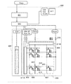
本実施の形態で例示する液晶表示装置800の各構成を、図5のブロック図に示す。液晶表示装置800は、画像処理回路801、タイミングコントローラ802、表示パネル803を有する。透過型液晶表示装置、又は半透過型液晶表示装置の場合、さらに光源としてバックライト部804を設ける。
Each structure of the liquid
液晶表示装置800は、接続された外部機器から画像信号(画像信号Data)が供給されている。なお、電源電位(高電源電位Vdd、低電源電位Vss、及び共通電位Vcom)は液晶表示装置の電源817をオン状態として電力供給を開始することによって供給され、制御信号(スタートパルスSP、及びクロック信号CK)はタイミングコントローラ802によって供給される。
The liquid
なお高電源電位Vddとは、基準電位より高い電位のことであり、低電源電位Vssとは基準電位以下の電位のことをいう。なお高電源電位Vdd及び低電源電位Vssともに、トランジスタが動作できる程度の電位であることが望ましい。なお高電源電位Vdd及び低電源電位Vssを併せて、電源電圧と呼ぶこともある。 Note that the high power supply potential Vdd is a potential higher than the reference potential, and the low power supply potential Vss is a potential lower than the reference potential. Note that it is desirable that both the high power supply potential Vdd and the low power supply potential Vss have such a potential that the transistor can operate. Note that the high power supply potential Vdd and the low power supply potential Vss may be collectively referred to as a power supply voltage.
共通電位Vcomは、一方の電極(画素電極)に供給される画像信号の電位に対して基準となる固定電位であればよく、一例としてはグラウンド電位であってもよい。 The common potential Vcom may be a fixed potential that serves as a reference with respect to the potential of the image signal supplied to one electrode (pixel electrode), and may be a ground potential as an example.
画像信号Dataは、ドット反転駆動、ソースライン反転駆動、ゲートライン反転駆動、フレーム反転駆動等に応じて適宜反転させて液晶表示装置800に入力される構成とすればよい。また、画像信号がアナログの信号の場合には、A/Dコンバータ等を介してデジタルの信号に変換して、液晶表示装置800に供給する構成とすればよい。
The image signal Data may be input to the liquid
本実施の形態では、液晶素子805の他方の電極(対向電極)及び容量素子813の一方の電極には、電源817よりタイミングコントローラ802を介して固定電位である共通電位Vcomが与えられている。
In this embodiment, a common potential Vcom that is a fixed potential is supplied from the
画像処理回路801は、入力される画像信号Dataを解析、演算、及び/または加工し、処理した画像信号Dataを判定信号と共にタイミングコントローラ802に出力する。
The
具体的には画像処理回路801は、入力される画像信号Dataを解析し動画であるか静止画であるかを判断し、判断結果を含む判定信号をタイミングコントローラ802に出力する。画像処理回路801は、静止画であれば、動画または静止画を含む画像信号Dataから1フレームの静止画を切り出し、静止画であることを意味する判定信号と共にタイミングコントローラ802に出力する。また、画像処理回路801は、動画であれば、入力される画像信号Dataを動画であることを意味する判定信号と共にタイミングコントローラ802に出力する。なお、上述した機能は画像処理回路801が有する機能の一例であり、表示装置の用途に応じて種々の画像処理機能を選択して適用すればよい。
Specifically, the
タイミングコントローラ802は、上記実施の形態1で述べた機能の他に、表示パネル803へ、処理した画像信号Data、並びに制御信号(具体的にはスタートパルスSP、及びクロック信号CK等の制御信号の供給または停止の切り替えを制御するための信号)、電源電位(高電源電位Vdd、低電源電位Vss、及び共通電位Vcom)を供給する回路である。
In addition to the functions described in
なお、デジタル信号に変換された画像信号は演算(例えば画像信号の差分を検出する等)が容易であるため、入力される画像信号(画像信号Data)がアナログの信号の場合には、A/Dコンバータ等を画像処理回路801に設ける構成とすればよい。
Since the image signal converted into the digital signal can be easily calculated (for example, detecting a difference between the image signals), when the input image signal (image signal Data) is an analog signal, A / A structure in which a D converter or the like is provided in the
表示パネル803は液晶素子805を一対の基板(第1の基板と第2の基板)間に挟持する構成を有し、第1の基板には駆動回路部806、画素部807が設けられる。また、第2の基板には共通接続部(コモンコンタクトともいう)、及び共通電極(コモン電極、または対向電極ともいう)が設けられる。なお、共通接続部は第1の基板と第2の基板とを電気的に接続するものであって、共通接続部は第1の基板上に設けられていてもよい。
The
画素部807には、複数のゲート線808(走査線)、及びソース線809(信号線)が設けられており、複数の画素810がゲート線808及びソース線809に環囲されてマトリクス状に設けられている。なお、本実施の形態で例示する表示パネルにおいては、ゲート線808はゲート線駆動回路811Aから延在し、ソース線809はソース線駆動回路811Bから延在している。
The
また、画素810はスイッチング素子としてトランジスタ812、該トランジスタ812に接続された容量素子813、及び液晶素子805を有する。
The
液晶素子805は、液晶の光学的変調作用によって光の透過又は非透過を制御する素子である。液晶の光学的変調作用は、液晶にかかる電界によって制御される。液晶にかかる電界方向は液晶材料、駆動方法、及び電極構造によって異なり、適宜選択することができる。例えば、液晶の厚さ方向(いわゆる縦方向)に電界をかける駆動方法を用いる場合は液晶を挟持するように第1の基板に画素電極を、第2の基板に共通電極をそれぞれ設ける構造とすればよい。また、液晶に基板面内方向(いわゆる横電界)に電界をかける駆動方法を用いる場合は、液晶に対して同一面に、画素電極と共通電極を設ける構造とすればよい。また画素電極及び共通電極は、多様な開口パターンを有する形状としてもよい。本実施の形態においては光学的変調作用によって光の透過又は非透過を制御する素子であれば、液晶材料、駆動方法、及び電極構造は特に限定されない。
The
トランジスタ812は、画素部807に設けられた複数のゲート線808のうちの一つとゲート電極が接続され、ソース電極またはドレイン電極の一方が複数のソース線809のうちの一つと接続され、ソース電極またはドレイン電極の他方が容量素子813の一方の電極、及び液晶素子805の一方の電極(画素電極)と接続される。
The
トランジスタ812は、オフ電流が低減されたトランジスタを用いることが好ましい。トランジスタ812がオフ状態のとき、オフ電流が低減されたトランジスタ812に接続された液晶素子805、及び容量素子813に蓄えられた電荷は、トランジスタ812を介して漏れ難く、トランジスタ812がオフ状態になる前に書き込まれた状態を、次に信号が書き込まれるまで安定して保持できる。従って、オフ電流が低減されたトランジスタ812に接続された容量素子813を用いることなく、画素810を構成することもできる。
As the
このような構成とすることで、容量素子813は液晶素子805に加える電圧を保持することができる。また、容量素子813の電極は、別途設けた容量線に接続する構成としてもよい。
With such a structure, the
駆動回路部806は、ゲート線駆動回路811A、ソース線駆動回路811Bを有する。ゲート線駆動回路811A、ソース線駆動回路811Bは、複数の画素を有する画素部807を駆動するための駆動回路であり、シフトレジスタ回路(シフトレジスタともいう)を有する。
The
なお、ゲート線駆動回路811A、及びソース線駆動回路811Bは、画素部807と同じ基板に形成されるものでもよいし、別の基板に形成されるものであってもよい。
Note that the gate
なお駆動回路部806には、タイミングコントローラ802によって制御された高電源電位Vdd、低電源電位Vss、スタートパルスSP、クロック信号CK、画像信号Dataが供給される。
Note that a high power supply potential Vdd, a low power supply potential Vss, a start pulse SP, a clock signal CK, and an image signal Data that are controlled by the
端子部816は、タイミングコントローラ802が出力する所定の信号(高電源電位Vdd、低電源電位Vss、スタートパルスSP、クロック信号CK、画像信号Data、共通電位Vcom等)等を駆動回路部806に供給する入力端子である。
The
また、液晶表示装置は、測光回路を有していてもよい。測光回路を設けた液晶表示装置は当該液晶表示装置がおかれている環境の明るさを検知できる。その結果、測光回路が接続されたタイミングコントローラ802は、測光回路から入力される信号に応じて、バックライト、サイドライト等の光源の駆動方法を制御することができる。
The liquid crystal display device may have a photometric circuit. A liquid crystal display device provided with a photometric circuit can detect the brightness of the environment in which the liquid crystal display device is placed. As a result, the
バックライト部804はバックライト制御回路814、及びバックライト815を有する。バックライト815は、液晶表示装置800の用途に応じて選択して組み合わせればよく、発光ダイオード(LED)などを用いることができる。バックライト815には例えば白色の発光素子(例えばLED)を配置することができる。バックライト制御回路814には、タイミングコントローラ802からバックライトを制御するバックライト信号、及び電源電位が供給される。
The
なお、カラー表示を行う場合は、カラーフィルタを組み合わせることで表示が可能である。また、他の光学フィルム(偏光フィルム、位相差フィルム、反射防止フィルムなど)も組み合わせて用いることができる。透過型液晶表示装置、又は半透過型液晶表示装置の場合に用いられるバックライト等の光源は、液晶表示装置800の用途に応じて選択して組み合わせればよく、冷陰極管や発光ダイオード(LED)などを用いることができる。また複数のLED光源、または複数のエレクトロルミネセンス(EL)光源などを用いて面光源を構成してもよい。面光源として、3種類以上のLEDを用いてもよいし、白色発光のLEDを用いてもよい。なお、バックライトにRGBの発光ダイオード等を配置し、時分割によりカラー表示する継時加法混色法(フィールドシーケンシャル法)を採用するときには、カラーフィルタを設けない場合もある。
In addition, when performing color display, it can display by combining a color filter. Also, other optical films (polarizing film, retardation film, antireflection film, etc.) can be used in combination. A light source such as a backlight used in the case of a transmissive liquid crystal display device or a transflective liquid crystal display device may be selected and combined depending on the application of the liquid
次に、画素に供給する信号の様子を、図5に示す画素の回路図、及び図6に示すタイミングチャートを用いて説明する。 Next, a state of a signal supplied to the pixel will be described with reference to a circuit diagram of the pixel shown in FIG. 5 and a timing chart shown in FIG.
図6に、タイミングコントローラ802がゲート線駆動回路811Aに供給するクロック信号GCK、及びスタートパルスGSPを示す。また、タイミングコントローラ802がソース線駆動回路811Bに供給するクロック信号SCK、及びスタートパルスSSPを示す。なお、クロック信号の出力のタイミングを説明するために、図6ではクロック信号の波形を単純な矩形波で示す。
FIG. 6 shows a clock signal GCK and a start pulse GSP that the
また図6に、ソース線809の電位(Data line)、画素電極の電位、並びに共通電極の電位を示す。 FIG. 6 shows the potential of the source line 809 (Data line), the potential of the pixel electrode, and the potential of the common electrode.
図6において期間901は、動画を表示するための画像信号を書き込む期間に相当する。期間901では画像信号、共通電位が画素部807の各画素、共通電極に供給されるように動作する。
In FIG. 6, a
また、期間902は、静止画を表示する期間に相当する。期間902では、画素部807の各画素への画像信号、共通電極への共通電位を停止することとなる。なお図6に示す期間902では、駆動回路部の動作を停止するよう各信号を供給する構成について示したが、期間902の長さ及びリフレッシュレートによって、定期的に画像信号を書き込むことで静止画の画質の劣化を防ぐ構成とすることが好ましい。このリフレッシュレートを上記実施の形態1で示した構成とすることで、階調が変化することによる画質の劣化を小さくすることができる。
A
まず、期間901におけるタイミングチャートを説明する。期間901では、クロック信号GCKとして、常時クロック信号が供給され、スタートパルスGSPとして、垂直同期周波数に応じたパルスが供給される。また、期間901では、クロック信号SCKとして、常時クロック信号が供給され、スタートパルスSSPとして、1ゲート選択期間に応じたパルスが供給される。
First, a timing chart in the
また、各行の画素に画像信号Dataがソース線809を介して供給され、ゲート線808の電位に応じて画素電極にソース線809の電位が供給される。
Further, the image signal Data is supplied to the pixels in each row through the
一方、期間902は、静止画を表示する期間である。次に、期間902におけるタイミングチャートを説明する。期間902では、クロック信号GCK、スタートパルスGSP、クロック信号SCK、及びスタートパルスSSPは共に停止する。また、期間902において、ソース線809に供給していた画像信号Dataは停止する。クロック信号GCK及びスタートパルスGSPが共に停止する期間902では、トランジスタ812が非導通状態となり画素電極の電位が浮遊状態となる。
On the other hand, the
期間902では、液晶素子805の両端の電極、即ち画素電極及び共通電極の電位を浮遊状態にして、新たに電位を供給することなく、静止画の表示を行うことができる。
In the
また、ゲート線駆動回路811A、及びソース線駆動回路811Bに供給するクロック信号、及びスタートパルスを停止することにより低消費電力化を図ることができる。
In addition, power consumption can be reduced by stopping the clock signal and the start pulse supplied to the gate
特に、トランジスタ812をオフ電流が低減されたトランジスタを用いることにより、液晶素子805の両端子に加わる電圧が経時的に低下する現象を抑制できる。
In particular, the use of a transistor with reduced off-state current as the
次に、動画から静止画に切り替わる期間(図6中の期間903)、及び静止画から動画に切り替わる期間(図6中の期間904)におけるパネルコントローラの動作を、図7(A)、(B)を用いて説明する。図7(A)、(B)はパネルコントローラが出力する、高電源電位Vdd、クロック信号(ここではGCK)、及びスタートパルス信号(ここではGSP)の電位を示す。
Next, the operation of the panel controller in the period for switching from a moving image to a still image (
動画から静止画に切り替わる期間903のパネルコントローラの動作を図7(A)に示す。パネルコントローラは、スタートパルスGSPを停止する(図7(A)のE1、第1のステップ)。次いで、スタートパルス信号GSPの停止後、パルス出力がシフトレジスタの最終段まで達した後に、複数のクロック信号GCKを停止する(図7(A)のE2、第2のステップ)。次いで、電源電圧の高電源電位Vddを低電源電位Vssにする(図7(A)のE3、第3のステップ)。
FIG. 7A shows the operation of the panel controller in the
以上の手順をもって、駆動回路部806の誤動作を引き起こすことなく、駆動回路部806に供給する信号を停止できる。動画から静止画に切り替わる際の誤動作はノイズを生じ、ノイズは静止画として保持されるため、誤動作が少ないパネルコントローラを搭載した液晶表示装置は、階調が変化することによる画質の劣化が少ない静止画を表示できる。
With the above procedure, the signal supplied to the
なお信号の停止とは、配線への所定の電位の供給を停止し、所定の固定電位が供給される配線、例えば低電源電位Vssが供給された配線、に接続することをいう。 Note that the stop of the signal means that the supply of a predetermined potential to the wiring is stopped and the wiring is connected to a wiring supplied with a predetermined fixed potential, for example, a wiring supplied with the low power supply potential Vss.
次に静止画から動画に切り替わる期間904のパネルコントローラの動作を図7(B)に示す。パネルコントローラは、電源電圧を低電源電位Vssから高電源電位Vddにする(図7(B)のS1、第1のステップ)。次いで、クロック信号GCKとして先にハイの電位を与えた後、複数のクロック信号GCKを供給する(図7(B)のS2、第2のステップ)。次いでスタートパルス信号GSPを供給する(図7(B)のS3、第3のステップ)。
Next, FIG. 7B illustrates the operation of the panel controller in the
以上の手順をもって、駆動回路部806の誤動作を引き起こすことなく駆動回路部806に駆動信号の供給を再開できる。各配線の電位を適宜順番に動画表示時に戻すことで、誤動作なく駆動回路部の駆動を行うことができる。
With the above procedure, the supply of the drive signal to the
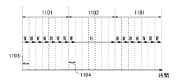
また、図8に、動画を表示する期間1101、または静止画を表示する期間1102における、フレーム期間毎の画像信号の書き込み頻度を模式的に示す。図8中、「W」は画像信号の書き込み期間であることをあらわし、「H」は画像信号を保持する期間であることを示している。また、図8中、期間1103は1フレーム期間を表したものであるが、別の期間であってもよい。
FIG. 8 schematically shows the frequency of writing image signals for each frame period in a
このように、本実施の形態の液晶表示装置の構成において、期間1102で表示される静止画の画像信号は期間1104に書き込まれ、期間1104で書き込まれた画像信号は、期間1102の他の期間で保持される。
As described above, in the structure of the liquid crystal display device in this embodiment, the still image signal displayed in the
本実施の形態に例示した液晶表示装置は、静止画を表示する期間において画像信号の書き込み頻度を低減できる。その結果、静止画を表示する際の低消費電力化を図ることができる。 The liquid crystal display device exemplified in this embodiment can reduce the frequency of writing image signals in a period during which a still image is displayed. As a result, it is possible to reduce power consumption when displaying a still image.
また、同一の画像を複数回書き換えて静止画を表示する場合、画像の切り替わりが視認できると、人間は目に疲労を感じることもあり得る。本実施の形態の液晶表示装置は、画像信号の書き込み頻度が削減されているため、目の疲労を減らすといった効果もある。 In addition, when a still image is displayed by rewriting the same image a plurality of times, if the switching of images can be visually recognized, humans may feel tired in the eyes. The liquid crystal display device of this embodiment has an effect of reducing eye fatigue because the frequency of writing image signals is reduced.
特に、本実施の形態の液晶表示装置は、オフ電流が低減されたトランジスタを各画素、並びに共通電極のスイッチング素子に適用することにより、保持容量で電圧を保持する期間(時間)を長く取ることができる。その結果、画像信号の書き込み頻度を小さくすることが可能になり、静止画を表示する際の低消費電力化、及び目の疲労の低減に、顕著な効果を有する。 In particular, in the liquid crystal display device in this embodiment, a transistor whose off-state current is reduced is applied to each pixel and the switching element of the common electrode, so that a period (time) in which the voltage is held in the storage capacitor is long. Can do. As a result, it is possible to reduce the frequency of writing image signals, which has a remarkable effect in reducing power consumption and reducing eye fatigue when displaying a still image.
(実施の形態3)
本実施の形態では、本明細書に開示する液晶表示装置に適用できるトランジスタの例を示す。
(Embodiment 3)
In this embodiment, an example of a transistor that can be applied to the liquid crystal display device disclosed in this specification will be described.
図9(A)乃至(D)にトランジスタの断面構造の一例を示す。 FIGS. 9A to 9D illustrate an example of a cross-sectional structure of the transistor.
図9(A)に示すトランジスタ1210は、ボトムゲート構造のトランジスタの一つであり、逆スタガ型トランジスタともいう。
A
トランジスタ1210は、絶縁表面を有する基板1200上に、ゲート電極層1201、ゲート絶縁層1202、半導体層1203、ソース電極層1205a、及びドレイン電極層1205bを含む。また、トランジスタ1210を覆い、半導体層1203に積層する絶縁層1207が設けられている。絶縁層1207上にはさらに保護絶縁層1209が形成されている。
The
図9(B)に示すトランジスタ1220は、チャネル保護型(チャネルストップ型ともいう)と呼ばれるボトムゲート構造の一つであり逆スタガ型トランジスタともいう。
A
トランジスタ1220は、絶縁表面を有する基板1200上に、ゲート電極層1201、ゲート絶縁層1202、半導体層1203、半導体層1203のチャネル形成領域上に設けられたチャネル保護層として機能する絶縁層1227、ソース電極層1205a、及びドレイン電極層1205bを含む。また、トランジスタ1220を覆い、保護絶縁層1209が形成されている。
The
図9(C)示すトランジスタ1230はボトムゲート型のトランジスタであり、絶縁表面を有する基板である基板1200上に、ゲート電極層1201、ゲート絶縁層1202、ソース電極層1205a、ドレイン電極層1205b、及び半導体層1203を含む。また、トランジスタ1230を覆い、半導体層1203に接する絶縁層1207が設けられている。絶縁層1207上にはさらに保護絶縁層1209が形成されている。
A
トランジスタ1230においては、ゲート絶縁層1202は基板1200及びゲート電極層1201上に接して設けられ、ゲート絶縁層1202上にソース電極層1205a、ドレイン電極層1205bが接して設けられている。そして、ゲート絶縁層1202、及びソース電極層1205a、ドレイン電極層1205b上に半導体層1203が設けられている。
In the
図9(D)に示すトランジスタ1240は、トップゲート構造のトランジスタの一つである。トランジスタ1240は、絶縁表面を有する基板1200上に、絶縁層1247、半導体層1203、ソース電極層1205a、及びドレイン電極層1205b、ゲート絶縁層1202、ゲート電極層1201を含み、ソース電極層1205a、ドレイン電極層1205bにそれぞれ配線層1246a、配線層1246bが接して設けられ電気的に接続している。
A
本実施の形態では、半導体層1203として酸化物半導体を用いる。
In this embodiment, an oxide semiconductor is used for the
酸化物半導体としては、四元系金属酸化物であるIn−Sn−Ga−Zn−O系金属酸化物や、三元系金属酸化物であるIn−Ga−Zn−O系金属酸化物、In−Sn−Zn−O系金属酸化物、In−Al−Zn−O系金属酸化物、Sn−Ga−Zn−O系金属酸化物、Al−Ga−Zn−O系金属酸化物、Sn−Al−Zn−O系金属酸化物や、二元系金属酸化物であるIn−Zn−O系金属酸化物、Sn−Zn−O系金属酸化物、Al−Zn−O系金属酸化物、Zn−Mg−O系金属酸化物、Sn−Mg−O系金属酸化物、In−Mg−O系金属酸化物や、In−O系、Sn−O系金属酸化物、Zn−O系金属酸化物などを用いることができる。また、上記金属酸化物の半導体にSiO2を含んでもよい。ここで、例えば、In−Ga−Zn−O系金属酸化物とは、少なくともInとGaとZnを含む酸化物であり、その組成比に特に制限はない。また、InとGaとZn以外の元素を含んでもよい。 As the oxide semiconductor, an In—Sn—Ga—Zn—O-based metal oxide that is a quaternary metal oxide, an In—Ga—Zn—O-based metal oxide that is a ternary metal oxide, In -Sn-Zn-O-based metal oxide, In-Al-Zn-O-based metal oxide, Sn-Ga-Zn-O-based metal oxide, Al-Ga-Zn-O-based metal oxide, Sn-Al -Zn-O-based metal oxides, binary metal oxides such as In-Zn-O-based metal oxides, Sn-Zn-O-based metal oxides, Al-Zn-O-based metal oxides, Zn- Mg-O-based metal oxide, Sn-Mg-O-based metal oxide, In-Mg-O-based metal oxide, In-O-based, Sn-O-based metal oxide, Zn-O-based metal oxide, etc. Can be used. The metal oxide semiconductor may contain SiO 2 . Here, for example, an In—Ga—Zn—O-based metal oxide is an oxide containing at least In, Ga, and Zn, and there is no particular limitation on the composition ratio thereof. Moreover, elements other than In, Ga, and Zn may be included.
また、酸化物半導体は、化学式InMO3(ZnO)m(m>0)で表記される薄膜を用いることができる。ここで、Mは、Ga、Al、MnおよびCoから選ばれた一または複数の金属元素を示す。例えばMとして、Ga、Ga及びAl、Ga及びMn、またはGa及びCoなどがある。 As the oxide semiconductor, a thin film represented by the chemical formula, InMO 3 (ZnO) m (m> 0) can be used. Here, M represents one or more metal elements selected from Ga, Al, Mn, and Co. For example, M includes Ga, Ga and Al, Ga and Mn, or Ga and Co.
なお本実施の形態の構成において酸化物半導体は、n型不純物である水素を酸化物半導体から除去し、酸化物半導体の主成分以外の不純物が極力含まれないように高純度化することにより真性(i型)とし、又は真性型としたものである。すなわち、不純物を添加してi型化するのでなく、水素や水等の不純物を極力除去したことにより、高純度化されたi型(真性半導体)又はそれに近づけたものである。加えて、酸化物半導体は、2.0eV以上、好ましくは2.5eV以上、より好ましくは3.0eV以上のバンドギャップを有する。そのため、酸化物半導体は、熱励起に起因するキャリアの発生を抑制することができる。その結果、酸化物半導体によってチャネル形成領域が構成されたトランジスタの動作温度の上昇に伴うオフ電流の増加を低減することができる。 Note that in the structure of this embodiment, the oxide semiconductor is intrinsic by removing hydrogen, which is an n-type impurity, from the oxide semiconductor and highly purified so that impurities other than the main component of the oxide semiconductor are included as much as possible. (I-type) or intrinsic type. That is, it is not made i-type by adding impurities, but is made highly purified i-type (intrinsic semiconductor) or close to it by removing impurities such as hydrogen and water as much as possible. In addition, the oxide semiconductor has a band gap of 2.0 eV or more, preferably 2.5 eV or more, more preferably 3.0 eV or more. Therefore, the oxide semiconductor can suppress generation of carriers due to thermal excitation. As a result, an increase in off-state current accompanying an increase in operating temperature of a transistor in which a channel formation region is formed using an oxide semiconductor can be reduced.
また、高純度化された酸化物半導体中にはキャリアが極めて少なく(ゼロに近い)、キャリア濃度は1×10¹⁴/cm3未満、好ましくは1×1012/cm3未満、さらに好ましくは1×1011/cm3未満である。 The highly purified oxide semiconductor has very few carriers (close to zero), and the carrier concentration is less than 1 × 10 14 / cm 3 , preferably less than 1 × 10 12 / cm 3 , and more preferably 1 It is less than × 10 11 / cm 3 .
酸化物半導体中にキャリアが極めて少ないため、トランジスタのオフ電流を少なくすることができる。具体的には、上述の酸化物半導体を半導体層に用いたトランジスタは、チャネル幅1μmあたりのオフ電流を10aA/μm(1×10−17A/μm)以下にすること、さらには1aA/μm(1×10−18A/μm)以下、さらには10zA/μm(1×10−20A/μm)にすることが可能である。つまりトランジスタの非導通状態において、酸化物半導体は絶縁体とみなせて回路設計を行うことができる。一方で、酸化物半導体は、トランジスタの導通状態においては、非晶質シリコンで形成される半導体層よりも高い電流供給能力を見込むことができる。 Since the number of carriers in the oxide semiconductor is extremely small, the off-state current of the transistor can be reduced. Specifically, a transistor in which the above oxide semiconductor is used for a semiconductor layer has an off-current per channel width of 1 μm of 10 aA / μm (1 × 10 −17 A / μm) or less, and further 1 aA / μm. (1 × 10 −18 A / μm) or less, further 10 zA / μm (1 × 10 −20 A / μm) is possible. That is, in the non-conducting state of the transistor, the oxide semiconductor can be regarded as an insulator and circuit design can be performed. On the other hand, an oxide semiconductor can expect a higher current supply capability than a semiconductor layer formed using amorphous silicon in a conductive state of a transistor.
酸化物半導体を半導体層1203に用いたトランジスタ1210、1220、1230、1240は、オフ状態における電流値(オフ電流値)を低くすることができる。よって、画像イメージデータ等の電気信号の保持時間を長くすることができ、書き込み間隔も長く設定できる。よって、リフレッシュレートを小さくすることができるため、より消費電力を抑制する効果を高くできる。
The
また、酸化物半導体を半導体層1203に用いたトランジスタ1210、1220、1230、1240は、非晶質半導体を用いたものとしては比較的高い電界効果移動度が得られるため、高速駆動が可能である。よって、表示装置の高機能化及び高速応答化が実現できる。
In addition, the
絶縁表面を有する基板1200に使用することができる基板に大きな制限はないが、少なくとも、後の加熱処理に耐えうる程度の耐熱性を有していることが必要となる。バリウムホウケイ酸ガラスやアルミノホウケイ酸ガラスなどのガラス基板を用いることができる。
There is no particular limitation on a substrate that can be used as the
また、ガラス基板としては、後の加熱処理の温度が高い場合には、歪み点が730℃以上のものを用いると良い。また、ガラス基板には、例えば、アルミノシリケートガラス、アルミノホウケイ酸ガラス、バリウムホウケイ酸ガラスなどのガラス材料が用いられている。なお、実用的な耐熱ガラスである、酸化ホウ素(B2O3)より酸化バリウム(BaO)を多く含むガラス基板を用いてもよい。 As the glass substrate, a glass substrate having a strain point of 730 ° C. or higher is preferably used when the temperature of the subsequent heat treatment is high. For the glass substrate, for example, a glass material such as aluminosilicate glass, aluminoborosilicate glass, or barium borosilicate glass is used. Note that a glass substrate containing more barium oxide (BaO) than boron oxide (B 2 O 3 ), which is a practical heat-resistant glass, may be used.
なお、上記のガラス基板に代えて、セラミック基板、石英基板、サファイア基板などの絶縁体でなる基板を用いても良い。他にも、結晶化ガラスなどを用いることができる。また、プラスチック基板等も適宜用いることができる。 Note that a substrate formed of an insulator such as a ceramic substrate, a quartz substrate, or a sapphire substrate may be used instead of the glass substrate. In addition, crystallized glass or the like can be used. A plastic substrate or the like can also be used as appropriate.
ボトムゲート構造のトランジスタ1210、1220、1230において、下地膜となる絶縁膜を基板とゲート電極層の間に設けてもよい。下地膜は、基板からの不純物元素の拡散を防止する機能があり、窒化シリコン膜、酸化シリコン膜、窒化酸化シリコン膜、又は酸化窒化シリコン膜から選ばれた一又は複数の膜による積層構造により形成することができる。
In the
ゲート電極層1201の材料は、モリブデン、チタン、クロム、タンタル、タングステン、アルミニウム、銅、ネオジム、スカンジウム等の金属材料またはこれらを主成分とする合金材料を用いて、単層でまたは積層して形成することができる。
The material of the
例えば、ゲート電極層1201の2層の積層構造としては、アルミニウム層上にモリブデン層が積層された2層の積層構造、または銅層上にモリブデン層を積層した2層構造、または銅層上に窒化チタン層若しくは窒化タンタルを積層した2層構造、窒化チタン層とモリブデン層とを積層した2層構造とすることが好ましい。3層の積層構造としては、タングステン層または窒化タングステンと、アルミニウムとシリコンの合金層またはアルミニウムとチタンの合金層と、窒化チタン層またはチタン層とを積層した積層とすることが好ましい。なお、透光性を有する導電膜を用いてゲート電極層を形成することもできる。透光性を有する導電膜としては、透光性導電性酸化物等をその例に挙げることができる。
For example, as a two-layer structure of the
ゲート絶縁層1202は、プラズマCVD法又はスパッタリング法等を用いて、酸化シリコン層、窒化シリコン層、酸化窒化シリコン層、窒化酸化シリコン層、酸化アルミニウム層、窒化アルミニウム層、酸化窒化アルミニウム層、窒化酸化アルミニウム層、又は酸化ハフニウム層を単層で又は積層して形成することができる。
The
ゲート絶縁層1202は、ゲート電極層側から窒化シリコン層と酸化シリコン層を積層した構造とすることもできる。例えば、第1のゲート絶縁層としてスパッタリング法により膜厚50nm以上200nm以下の窒化シリコン層(SiNy(y>0))を形成し、第1のゲート絶縁層上に第2のゲート絶縁層として膜厚5nm以上300nm以下の酸化シリコン層(SiOx(x>0))を積層して、膜厚100nmのゲート絶縁層とする。ゲート絶縁層1202の膜厚は、トランジスタに要求される特性によって適宜設定すればよく350nm乃至400nm程度でもよい。
The
ソース電極層1205a、ドレイン電極層1205bに用いる導電膜としては、例えば、Al、Cr、Cu、Ta、Ti、Mo、Wからから選ばれた元素、または上述した元素を成分とする合金か、上述した元素を組み合わせた合金膜等を用いることができる。また、Al、Cuなどの金属層の下側又は上側の一方または双方にCr、Ta、Ti、Mo、Wなどの高融点金属層を積層させた構成としても良い。また、Si、Ti、Ta、W、Mo、Cr、Nd、Sc、YなどAl膜に生ずるヒロックやウィスカーの発生を防止する元素が添加されているAl材料を用いることで耐熱性を向上させることが可能となる。
As the conductive film used for the
ソース電極層1205a、ドレイン電極層1205bに接続する配線層1246a、配線層1246bのような導電膜も、ソース電極層1205a、ドレイン電極層1205bと同様な材料を用いることができる。
The conductive film such as the
また、ソース電極層1205a、ドレイン電極層1205bは、単層構造でも、2層以上の積層構造としてもよい。例えば、シリコンを含むアルミニウム膜の単層構造、アルミニウム膜上にチタン膜を積層する2層構造、Ti膜と、そのTi膜上に重ねてアルミニウム膜を積層し、さらにその上にTi膜を成膜する3層構造などが挙げられる。
The
また、ソース電極層1205a、ドレイン電極層1205b(これと同じ層で形成される配線層を含む)となる導電膜を導電性の金属酸化物で形成しても良い。導電性の金属酸化物としては酸化インジウム(In2O3)、酸化スズ(SnO2)、酸化亜鉛(ZnO)、酸化インジウム酸化スズ合金(In2O3―SnO2、ITOと略記する)、酸化インジウム酸化亜鉛合金(In2O3―ZnO)または前記金属酸化物材料にシリコン若しくは酸化シリコンを含ませたものを用いることができる。
Alternatively, the conductive film to be the
絶縁層1207、1227、1247、保護絶縁層1209としては、酸化絶縁層、又は窒化絶縁層などの無機絶縁膜を好適に用いることができる。
As the insulating
絶縁層1207、1227、1247は、代表的には酸化シリコン膜、酸化窒化シリコン膜、酸化アルミニウム膜、または酸化窒化アルミニウム膜などの無機絶縁膜を用いることができる。
As the insulating
保護絶縁層1209は、窒化シリコン膜、窒化アルミニウム膜、窒化酸化シリコン膜、窒化酸化アルミニウム膜などの無機絶縁膜を用いることができる。
As the protective insulating
また、保護絶縁層1209上にトランジスタ起因の表面凹凸を低減するために平坦化絶縁膜を形成してもよい。平坦化絶縁膜としては、ポリイミド、アクリル、ベンゾシクロブテン、ポリアミド、エポキシ等の、耐熱性を有する有機材料を用いることができる。また上記有機材料の他に、低誘電率材料(low−k材料)、シロキサン系樹脂、PSG(リンガラス)、BPSG(リンボロンガラス)等を用いることができる。なお、これらの材料で形成される絶縁膜を複数積層させることで、平坦化絶縁膜を形成してもよい。
Further, a planarization insulating film may be formed over the protective insulating
このように、本実施の形態において、酸化物半導体を半導体層に用いたトランジスタを用いることにより、さらに低消費電力化が達成された高機能な液晶表示装置を提供することができる。 As described above, in this embodiment, a high-performance liquid crystal display device in which lower power consumption is achieved can be provided by using a transistor in which an oxide semiconductor is used for a semiconductor layer.
本実施の形態は、他の実施の形態に記載した構成と適宜組み合わせて実施することが可能である。 This embodiment can be implemented in appropriate combination with the structures described in the other embodiments.
(実施の形態4)
トランジスタを作製し、該トランジスタを画素部、さらには駆動回路に用いて表示機能を有する液晶表示装置を作製することができる。また、トランジスタを駆動回路の一部または全体を、画素部と同じ基板上に一体形成し、システムオンパネルを形成することができる。
(Embodiment 4)
A transistor is manufactured, and a liquid crystal display device having a display function can be manufactured using the transistor in a pixel portion and further in a driver circuit. In addition, a part or the whole of the driver circuit of the transistor can be formed over the same substrate as the pixel portion to form a system-on-panel.
なお液晶表示装置とは、コネクター、例えばFPC(Flexible printed circuit)もしくはTAB(Tape Automated Bonding)テープもしくはTCP(Tape Carrier Package)が取り付けられたモジュール、TABテープやTCPの先にプリント配線板が設けられたモジュール、または表示素子にCOG(Chip On Glass)方式によりIC(集積回路)が直接実装されたモジュールも全て表示装置に含むものとする。 A liquid crystal display device is a module in which a connector, for example, an FPC (Flexible printed circuit) or TAB (Tape Automated Bonding) tape or TCP (Tape Carrier Package) is attached, and a printed wiring board is provided at the end of the TAB tape or TCP. In addition, all the modules in which an IC (integrated circuit) is directly mounted on a display element or a display element by a COG (Chip On Glass) method are included in the display device.
液晶表示装置の外観及び断面について、図10(A1)、(A2)、および(B)を用いて説明する。図10(A1)、(A2)は、トランジスタ4010、4011、及び液晶素子4013を、第1の基板4001と第2の基板4006との間にシール材4005によって封止した、パネルの平面図であり、図10(B)は、図10(A1)(A2)のM−Nにおける断面図に相当する。
The appearance and a cross section of the liquid crystal display device will be described with reference to FIGS. 10A1, 10 </ b> A <b> 2, and 10 </ b> B. 10A1 and 10A2 are plan views of a panel in which the
第1の基板4001上に設けられた画素部4002と、走査線駆動回路4004とを囲むようにして、シール材4005が設けられている。また画素部4002と、走査線駆動回路4004の上に第2の基板4006が設けられている。よって画素部4002と、走査線駆動回路4004とは、第1の基板4001とシール材4005と第2の基板4006とによって、液晶層4008と共に封止されている。また第1の基板4001上のシール材4005によって囲まれている領域とは異なる領域に、別途用意された基板上に単結晶半導体膜又は多結晶半導体膜で形成された信号線駆動回路4003が実装されている。
A
なお、別途形成した駆動回路の接続方法は、特に限定されるものではなく、COG方法、ワイヤボンディング方法、或いはTAB方法などを用いることができる。図10(A1)は、COG方法により信号線駆動回路4003を実装する例であり、図10(A2)は、TAB方法により信号線駆動回路4003を実装する例である。
Note that a connection method of a driver circuit which is separately formed is not particularly limited, and a COG method, a wire bonding method, a TAB method, or the like can be used. FIG. 10A1 illustrates an example in which the signal
また第1の基板4001上に設けられた画素部4002と、走査線駆動回路4004は、トランジスタを複数有しており、図10(B)では、画素部4002に含まれるトランジスタ4010と、走査線駆動回路4004に含まれるトランジスタ4011とを例示している。トランジスタ4010、4011上には絶縁層4041a、4041b、4042a、4042b、4020、4021が設けられている。
In addition, the
トランジスタ4010、4011は、酸化物半導体を半導体層に用いたトランジスタを適用することができる。本実施の形態において、トランジスタ4010、4011はnチャネル型トランジスタである。
As the
絶縁層4021上において、駆動回路用のトランジスタ4011の酸化物半導体を用いたチャネル形成領域と重なる位置に導電層4040が設けられている。導電層4040を酸化物半導体を用いたチャネル形成領域と重なる位置に設けることによって、BT(Bias Temperature)試験前後におけるトランジスタ4011のしきい値電圧の変化量を低減することができる。また、導電層4040は、電位がトランジスタ4011のゲート電極層と同じでもよいし、異なっていても良く、第2のゲート電極層として機能させることもできる。また、導電層4040の電位がGND、0V、或いはフローティング状態であってもよい。
A
また、液晶素子4013が有する画素電極層4030は、トランジスタ4010と電気的に接続されている。そして液晶素子4013の対向電極層4031は第2の基板4006上に形成されている。画素電極層4030と対向電極層4031と液晶層4008とが重なっている部分が、液晶素子4013に相当する。なお、画素電極層4030、対向電極層4031はそれぞれ配向膜として機能する絶縁層4032、4033が設けられ、絶縁層4032、4033を介して液晶層4008を挟持している。
In addition, the
なお、第1の基板4001、第2の基板4006としては、透光性基板を用いることができ、ガラス、セラミックス、プラスチックを用いることができる。プラスチックとしては、FRP(Fiberglass−Reinforced Plastics)板、PVF(ポリビニルフルオライド)フィルム、ポリエステルフィルムまたはアクリル樹脂フィルムを用いることができる。
Note that a light-transmitting substrate can be used as the
また4035は絶縁膜を選択的にエッチングすることで得られる柱状のスペーサであり、画素電極層4030と対向電極層4031との間の距離(セルギャップ)を制御するために設けられている。なお球状のスペーサを用いていても良い。また、対向電極層4031は、トランジスタ4010と同一基板上に設けられる共通電位線と電気的に接続される。共通接続部を用いて、一対の基板間に配置される導電性粒子を介して対向電極層4031と共通電位線とを電気的に接続することができる。なお、導電性粒子はシール材4005に含有させることができる。
また、配向膜を用いないブルー相を示す液晶を用いてもよい。ブルー相は液晶相の一つであり、コレステリック液晶を昇温していくと、コレステリック相から等方相へ転移する直前に発現する相である。ブルー相は狭い温度範囲でしか発現しないため、温度範囲を改善するために5重量%以上のカイラル剤を混合させた液晶組成物を用いて液晶層4008に用いる。ブルー相を示す液晶とカイラル剤とを含む液晶組成物は、応答速度が1msec以下と短く、光学的等方性であるため配向処理が不要であり、視野角依存性が小さい。
Alternatively, a liquid crystal exhibiting a blue phase for which an alignment film is unnecessary may be used. The blue phase is one of the liquid crystal phases. When the temperature of the cholesteric liquid crystal is increased, the blue phase appears immediately before the transition from the cholesteric phase to the isotropic phase. Since the blue phase appears only in a narrow temperature range, a liquid crystal composition mixed with 5% by weight or more of a chiral agent is used for the
なお透過型液晶表示装置の他に、半透過型液晶表示装置でも適用できる。 In addition to the transmissive liquid crystal display device, a transflective liquid crystal display device can also be applied.
また、液晶表示装置では、基板の外側(視認側)に偏光板を設け、内側に着色層、表示素子に用いる電極層という順に設ける例を示すが、偏光板は基板の内側に設けてもよい。また、偏光板と着色層の積層構造も本実施の形態に限定されず、偏光板及び着色層の材料や作製工程条件によって適宜設定すればよい。また、表示部以外にブラックマトリクスとして機能する遮光膜を設けてもよい。 In the liquid crystal display device, a polarizing plate is provided on the outer side (viewing side) of the substrate, a colored layer is provided on the inner side, and an electrode layer used for the display element is provided in this order. . In addition, the stacked structure of the polarizing plate and the colored layer is not limited to this embodiment mode, and may be set as appropriate depending on the material and manufacturing process conditions of the polarizing plate and the colored layer. In addition to the display portion, a light shielding film functioning as a black matrix may be provided.
トランジスタ4011は、チャネル保護層として機能する絶縁層4041aと、酸化物半導体を用いた半導体層の積層の周縁部(側面を含む)を覆う絶縁層4041bとが形成されている。同様にトランジスタ4010は、チャネル保護層として機能する絶縁層4042aと、酸化物半導体を用いた半導体層の積層の周縁部(側面を含む)を覆う絶縁層4042bとが形成されている。
In the
酸化物半導体を用いた半導体層の周縁部(側面を含む)を覆う酸化物絶縁層である絶縁層4041b、4042bは、ゲート電極層と、その上方または周辺に形成される配線層(ソース配線層や容量配線層など)との距離を大きくし、寄生容量の低減を図ることができる。また、トランジスタの表面凹凸を低減するため平坦化絶縁膜として機能する絶縁層4021で覆う構成となっている。ここでは、絶縁層4041a、4041b、4042a、4042bとして、一例としてスパッタ法により酸化珪素膜を形成する。
Insulating
また、絶縁層4041a、4041b、4042a、4042b上に絶縁層4020が形成されている。絶縁層4020は、一例としてRFスパッタ法により窒化珪素膜を形成する。
An insulating
また、平坦化絶縁膜として絶縁層4021を形成する。絶縁層4021としては、ポリイミド、アクリル、ベンゾシクロブテン、ポリアミド、エポキシ等の、耐熱性を有する有機材料を用いることができる。また上記有機材料の他に、低誘電率材料(low−k材料)、シロキサン系樹脂、PSG(リンガラス)、BPSG(リンボロンガラス)等を用いることができる。なお、これらの材料で形成される絶縁膜を複数積層させることで、絶縁層4021を形成してもよい。
In addition, the insulating
本実施の形態では、画素部の複数のトランジスタをまとめて窒化物絶縁膜で囲む構成としてもよい。絶縁層4020とゲート絶縁層とに窒化物絶縁膜を用いて、少なくともアクティブマトリクス基板の画素部の周縁を囲むように絶縁層4020とゲート絶縁層とが接する領域を設ける構成とすればよい。この製造プロセスでは、外部からの水分の侵入を防ぐことができる。また、液晶表示装置としてデバイスが完成した後にも長期的に、外部からの水分の侵入を防ぐことができデバイスの長期信頼性を向上することができる。
In this embodiment, a plurality of transistors in the pixel portion may be collectively surrounded by a nitride insulating film. A nitride insulating film may be used for the insulating
なおシロキサン系樹脂とは、シロキサン系材料を出発材料として形成されたSi−O−Si結合を含む樹脂に相当する。シロキサン系樹脂は置換基としては有機基(例えばアルキル基やアリール基)やフルオロ基を用いても良い。また、有機基はフルオロ基を有していても良い。 Note that the siloxane-based resin corresponds to a resin including a Si—O—Si bond formed using a siloxane-based material as a starting material. Siloxane resins may use organic groups (for example, alkyl groups and aryl groups) and fluoro groups as substituents. The organic group may have a fluoro group.
絶縁層4021の形成法は、特に限定されず、その材料に応じて、スパッタ法、SOG法、スピンコート、ディップ、スプレー塗布、液滴吐出法(インクジェット法、スクリーン印刷、オフセット印刷等)、ドクターナイフ、ロールコーター、カーテンコーター、ナイフコーター等を用いることができる。絶縁層4021の焼成工程と半導体層のアニールを兼ねることで効率よく液晶表示装置を作製することが可能となる。
The formation method of the insulating
画素電極層4030、対向電極層4031は、酸化タングステンを含むインジウム酸化物、酸化タングステンを含むインジウム亜鉛酸化物、酸化チタンを含むインジウム酸化物、酸化チタンを含むインジウム錫酸化物、インジウム錫酸化物(以下、ITOと示す)、インジウム亜鉛酸化物、酸化ケイ素を添加したインジウム錫酸化物などの透光性の導電性材料を用いることができる。
The
また、画素電極層4030、対向電極層4031として、導電性高分子(導電性ポリマーともいう)を含む導電性組成物を用いて形成することができる。導電性組成物を用いて形成した画素電極は、シート抵抗が10000Ω/□以下、波長550nmにおける透光率が70%以上であることが好ましい。また、導電性組成物に含まれる導電性高分子の抵抗率が0.1Ω・cm以下であることが好ましい。
The
導電性高分子としては、いわゆるπ電子共役系導電性高分子が用いることができる。例えば、ポリアニリンまたはその誘導体、ポリピロールまたはその誘導体、ポリチオフェンまたはその誘導体、若しくはアリニン、ピロールおよびチオフェンの2種以上からなる共重合体若しくはその誘導体などがあげられる。 As the conductive polymer, a so-called π-electron conjugated conductive polymer can be used. For example, polyaniline or a derivative thereof, polypyrrole or a derivative thereof, polythiophene or a derivative thereof, a copolymer of two or more of arinin, pyrrole, and thiophene or a derivative thereof can be given.
また別途形成された信号線駆動回路4003と、走査線駆動回路4004または画素部4002に与えられる各種信号及び電位は、FPC4018から供給されている。
In addition, a variety of signals and potentials are supplied to the signal
接続端子電極4015が、液晶素子4013が有する画素電極層4030と同じ導電膜から形成され、端子電極4016は、トランジスタ4010、4011のソース電極層及びドレイン電極層と同じ導電膜で形成されている。
The
接続端子電極4015は、FPC4018が有する端子と、異方性導電膜4019を介して電気的に接続されている。
The
また図10(A1)、(A2)においては、信号線駆動回路4003を別途形成し、第1の基板4001に実装している例を示しているがこの構成に限定されない。走査線駆動回路を別途形成して実装しても良いし、信号線駆動回路の一部または走査線駆動回路の一部のみを別途形成して実装しても良い。
10A1 and 10A2 illustrate an example in which the signal
図11は、液晶表示装置を構成する一例を示している。 FIG. 11 shows an example of a liquid crystal display device.
図11は液晶表示装置の一例であり、TFT基板2600と対向基板2601がシール材2602により固着され、その間にTFT等を含む画素部2603、液晶層を含む表示素子2604、着色層2605が設けられ表示領域を形成している。着色層2605はカラー表示を行う場合に必要であり、RGB方式の場合は、赤、緑、青の各色に対応した着色層が各画素に対応して設けられている。TFT基板2600と対向基板2601の外側には偏光板2606、偏光板2607、拡散板2613が配設されている。光源は冷陰極管2610と反射板2611により構成される。回路基板2612は、フレキシブル配線基板2609によりTFT基板2600の配線回路部2608と接続され、コントロール回路や電源回路などの外部回路が組みこまれている。また偏光板と、液晶層との間に位相差板を有した状態で積層してもよい。
FIG. 11 illustrates an example of a liquid crystal display device. A
液晶表示装置の駆動方式には、TN(Twisted Nematic)モード、IPS(In−Plane−Switching)モード、FFS(Fringe Field Switching)モード、MVA(Multi−domain Vertical Alignment)モード、PVA(Patterned Vertical Alignment)モード、ASM(Axially Symmetric aligned Micro−cell)モード、OCB(Optically Compensated Birefringence)モード、FLC(Ferroelectric Liquid Crystal)モード、AFLC(AntiFerroelectric Liquid Crystal)などを用いることができる。 The driving method of the liquid crystal display device includes a TN (Twisted Nematic) mode, an IPS (In-Plane-Switching) mode, an FFS (Fringe Field Switching) mode, an MVA (Multi-domain Vertical Alignment) mode, and a PVA (Pattern Alignment). Mode, ASM (Axial Symmetrically Aligned Micro-cell) mode, OCB (Optically Compensated Birefringence) mode, FLC (Ferroelectric Liquid Crystal) mode, AFLC (Antiferrofluid Crystal) It can be used.
以上の工程により、静止画表示を行う際、階調が変化することによる画質の劣化を小さくすることができる液晶表示装置を作製することができる。 Through the above steps, a liquid crystal display device that can reduce deterioration in image quality due to a change in gradation when performing still image display can be manufactured.
本実施の形態は、他の実施の形態に記載した構成と適宜組み合わせて実施することが可能である。 This embodiment can be implemented in appropriate combination with the structures described in the other embodiments.
(実施の形態5)
本実施の形態では、上記実施の形態で示す液晶表示装置において、タッチパネル機能を付加した液晶表示装置の構成について、図12(A)、(B)を用いて説明する。
(Embodiment 5)
In this embodiment, a structure of a liquid crystal display device to which a touch panel function is added in the liquid crystal display device described in the above embodiment will be described with reference to FIGS.
図12(A)は、本実施の形態の液晶表示装置の概略図である。図12(A)には、上記実施の形態の液晶表示装置である液晶表示パネル1501にタッチパネルユニット1502を重畳して設け、筐体1503(ケース)にて合着させる構成について示している。タッチパネルユニット1502は、抵抗膜方式、表面型静電容量方式、投影型静電容量方式等を適宜用いることができる。
FIG. 12A is a schematic diagram of the liquid crystal display device of this embodiment. FIG. 12A illustrates a structure in which a
図12(A)に示すように、液晶表示パネル1501とタッチパネルユニット1502とを別々に作製し重畳することにより、タッチパネル機能を付加した液晶表示装置の作製に係るコストの削減を図ることができる。
As shown in FIG. 12A, the liquid
図12(A)とは異なるタッチパネル機能を付加した液晶表示装置の構成について、図12(B)に示す。図12(B)に示す液晶表示装置1504は、複数設けられる画素1505に光センサ1506、液晶素子1507を有する。そのため、図12(A)とは異なり、タッチパネルユニット1502を重畳して作製する必要がなく、液晶表示装置の薄型化を図ることができる。なお、画素1505とともにゲート線側駆動回路1508、信号線側駆動回路1509、光センサ用駆動回路1510を画素1505と同じ基板上に作製することで、液晶表示装置の小型化を図ることができる。なお光センサ1506は、アモルファスシリコン等で形成し、酸化物半導体を用いたトランジスタと重畳して形成する構成としてもよい。
FIG. 12B illustrates a structure of a liquid crystal display device to which a touch panel function different from that in FIG. A liquid
本実施の形態により、タッチパネルの機能を付加した液晶表示装置において、酸化物半導体膜を用いたトランジスタを用いることで、静止画の表示の際の、画像の保持特性を向上させることができる。そしてリフレッシュレートを低減して静止画表示を行う際、階調が変化することによる画質の劣化を小さくすることができる。 According to this embodiment, in a liquid crystal display device to which a touch panel function is added, by using a transistor including an oxide semiconductor film, image retention characteristics when a still image is displayed can be improved. When still image display is performed at a reduced refresh rate, it is possible to reduce deterioration in image quality due to a change in gradation.
なお、本実施の形態は、他の実施の形態と適宜組み合わせることができる。 Note that this embodiment can be combined with any of the other embodiments as appropriate.
(実施の形態6)
本実施の形態においては、上記実施の形態で説明した液晶表示装置を具備する電子機器の例について説明する。
(Embodiment 6)
In this embodiment, examples of electronic devices each including the liquid crystal display device described in the above embodiment will be described.
図13(A)は携帯型遊技機であり、筐体9630、表示部9631、スピーカ9633、操作キー9635、接続端子9636、記録媒体読込部9672、等を有することができる。図13(A)に示す携帯型遊技機は、記録媒体に記録されているプログラム又はデータを読み出して表示部に表示する機能、他の携帯型遊技機と無線通信を行って情報を共有する機能、等を有することができる。なお、図13(A)に示す携帯型遊技機が有する機能はこれに限定されず、様々な機能を有することができる。
FIG. 13A illustrates a portable game machine that can include a
図13(B)はデジタルカメラであり、筐体9630、表示部9631、スピーカ9633、操作キー9635、接続端子9636、シャッターボタン9676、受像部9677、等を有することができる。図13(B)に示すデジタルカメラは、静止画を撮影する機能、動画を撮影する機能、撮影した画像を自動または手動で補正する機能、アンテナから様々な情報を取得する機能、撮影した画像、又はアンテナから取得した情報を保存する機能、撮影した画像、又はアンテナから取得した情報を表示部に表示する機能、等を有することができる。なお、図13(B)に示すデジタルカメラが有する機能はこれに限定されず、様々な機能を有することができる。
FIG. 13B illustrates a digital camera which can include a
図13(C)はテレビ受像器であり、筐体9630、表示部9631、スピーカ9633、操作キー9635、接続端子9636、等を有することができる。図13(C)に示すテレビ受像機は、テレビ用電波を処理して画像信号に変換する機能、画像信号を処理して表示に適した信号に変換する機能、画像信号のフレーム周波数を変換する機能、等を有することができる。なお、図13(C)に示すテレビ受像機が有する機能はこれに限定されず、様々な機能を有することができる。
FIG. 13C illustrates a television receiver that can include a
図13(D)は、電子計算機(パーソナルコンピュータ)用途のモニター(PCモニターともいう)であり、筐体9630、表示部9631等を有することができる。図13(D)に示すモニターは、ウインドウ型表示部9653が表示部9631にある例について示している。なお説明のために表示部9631にウインドウ型表示部9653を示したが、他のシンボル、例えばアイコン、画像等であってもよい。パーソナルコンピュータ用途のモニターでは、入力時にのみ画像信号が書き換えられる場合が多く、上記実施の形態における液晶表示装置の駆動方法を適用する際に好適である。なお、図13(D)に示すモニターが有する機能はこれに限定されず、様々な機能を有することができる。
FIG. 13D illustrates a monitor (also referred to as a PC monitor) for use in an electronic computer (personal computer), which can include a
図14(A)はコンピュータであり、筐体9630、表示部9631、スピーカ9633、操作キー9635、接続端子9636、ポインティングデバイス9681、外部接続ポート9680等を有することができる。図14(A)に示すコンピュータは、様々な情報(静止画、動画、テキスト画像など)を表示部に表示する機能、様々なソフトウェア(プログラム)によって処理を制御する機能、無線通信又は有線通信などの通信機能、通信機能を用いて様々なコンピュータネットワークに接続する機能、通信機能を用いて様々なデータの送信又は受信を行う機能、等を有することができる。なお、図14(A)に示すコンピュータが有する機能はこれに限定されず、様々な機能を有することができる。
FIG. 14A illustrates a computer which can include a
次に、図14(B)は携帯電話であり、筐体9630、表示部9631、スピーカ9633、操作キー9635、マイクロフォン9638等を有することができる。図14(B)に示した携帯電話は、様々な情報(静止画、動画、テキスト画像など)を表示する機能、カレンダー、日付又は時刻などを表示部に表示する機能、表示部に表示した情報を操作又は編集する機能、様々なソフトウェア(プログラム)によって処理を制御する機能、等を有することができる。なお、図14(B)に示した携帯電話が有する機能はこれに限定されず、様々な機能を有することができる。
Next, FIG. 14B illustrates a cellular phone, which can include a
次に、図14(C)は電子ペーパー(E−bookともいう)であり、筐体9630、表示部9631、操作キー9632等を有することができる。図14(C)に示した電子ペーパーは、様々な情報(静止画、動画、テキスト画像など)を表示する機能、カレンダー、日付又は時刻などを表示部に表示する機能、表示部に表示した情報を操作又は編集する機能、様々なソフトウェア(プログラム)によって処理を制御する機能、等を有することができる。なお、図14(C)に示した電子ペーパーが有する機能はこれに限定されず、様々な機能を有することができる。別の電子ペーパーの構成について図14(D)に示す。図14(D)に示す電子ペーパーは、図14(C)の電子ペーパーに太陽電池9651、及びバッテリー9652を付加した構成について示している。表示部9631として反射型の液晶表示装置を用いる場合、比較的明るい状況下での使用が予想され、太陽電池9651による発電、及びバッテリー9652での充電を効率よく行うことができ、好適である。なおバッテリー9652としては、リチウムイオン電池を用いると、小型化を図れる等の利点がある。
Next, FIG. 14C illustrates electronic paper (also referred to as E-book), which can include a
本実施の形態において述べた電子機器は、リフレッシュレートを低減して静止画表示を行う際、階調が変化することによる画質の劣化を小さくすることができる。 The electronic device described in this embodiment can reduce deterioration in image quality due to a change in gradation when a still image is displayed at a reduced refresh rate.
本実施の形態は、他の実施の形態に記載した構成と適宜組み合わせて実施することが可能である。 This embodiment can be implemented in appropriate combination with the structures described in the other embodiments.
100 液晶表示装置
101 タイミングコントローラ
102 駆動回路
103 表示部
104 動画表示期間
105 静止画表示期間
106 期間
107 期間
108 期間
109 期間
110 期間
111 期間
201 1階調
202 2階調
203 3階調
204 4階調
205 M階調
211 1階調
212 2階調
213 N階調
301 (i−2)階調
302 (i−1)階調
303 i階調
304 (i+1)階調
305 (i+2)階調
306 階調
307 矢印
311 (j−1)階調
312 j階調
313 (j+1)階調
314 階調
315 矢印
401 分析部
402 ルックアップテーブル部
403 パネルコントローラ
411 カウンタ回路
412 判定部
800 液晶表示装置
801 画像処理回路
802 タイミングコントローラ
803 表示パネル
804 バックライト部
805 液晶素子
806 駆動回路部
807 画素部
808 ゲート線
809 ソース線
810 画素
811A ゲート線駆動回路
811B ソース線駆動回路
812 トランジスタ
813 容量素子
814 バックライト制御回路
815 バックライト
816 端子部
817 電源
901 期間
902 期間
903 期間
904 期間
1101 期間
1102 期間
1103 期間
1104 期間
1200 基板
1201 ゲート電極層
1202 ゲート絶縁層
1203 半導体層
1205a ソース電極層
1205b ドレイン電極層
1207 絶縁層
1209 保護絶縁層
1210 トランジスタ
1220 トランジスタ
1227 絶縁層
1230 トランジスタ
1240 トランジスタ
1246a 配線層
1246b 配線層
1247 絶縁層
1501 液晶表示パネル
1502 タッチパネルユニット
1503 筐体
1504 液晶表示装置
1505 画素
1506 光センサ
1507 液晶素子
1508 ゲート線駆動回路
1509 信号線駆動回路
1510 光センサ用駆動回路
2600 TFT基板
2601 対向基板
2602 シール材
2603 画素部
2604 表示素子
2605 着色層
2606 偏光板
2607 偏光板
2608 配線回路部
2609 フレキシブル配線基板
2610 冷陰極管
2611 反射板
2612 回路基板
2613 拡散板
4001 基板
4002 画素部
4003 信号線駆動回路
4004 走査線駆動回路
4005 シール材
4006 基板
4008 液晶層
4010 トランジスタ
4011 トランジスタ
4013 液晶素子
4015 接続端子電極
4016 端子電極
4018 FPC
4019 異方性導電膜
4020 絶縁層
4021 絶縁層
4030 画素電極層
4031 対向電極層
4032 絶縁層
4033 絶縁層
4040 導電層
4041a 絶縁層
4041b 絶縁層
4042a 絶縁層
4042b 絶縁層
9630 筐体
9631 表示部
9632 操作キー
9633 スピーカ
9635 操作キー
9636 接続端子
9638 マイクロフォン
9651 太陽電池
9652 バッテリー
9653 ウインドウ型表示部
9672 記録媒体読込部
9676 シャッターボタン
9677 受像部
9680 外部接続ポート
9681 ポインティングデバイス
100 liquid crystal display device 101 timing controller 102 drive circuit 103 display unit 104 moving image display period 105 still image display period 106 period 107 period 108 period 109 period 110 period 111 period 201 1 gradation 202 2 gradation 203 3 gradation 204 4 gradation 205 M gradation 211 1 gradation 212 2 gradation 213 N gradation 301 (i-2) gradation 302 (i-1) gradation 303 i gradation 304 (i + 1) gradation 305 (i + 2) gradation 306 Key 307 Arrow 311 (j-1) Gradation 312 j Gradation 313 (j + 1) Gradation 314 Gradation 315 Arrow 401 Analysis unit 402 Look-up table unit 403 Panel controller 411 Counter circuit 412 Determination unit 800 Liquid crystal display device 801 Image processing Circuit 802 Timing controller 803 Display panel 804 Buckler 805 Liquid crystal element 806 Drive circuit portion 807 Pixel portion 808 Gate line 809 Source line 810 Pixel 811A Gate line drive circuit 811B Source line drive circuit 812 Transistor 813 Capacitance element 814 Backlight control circuit 815 Backlight 816 Terminal portion 817 Power source 901 Period 902 period 903 period 904 period 1101 period 1102 period 1103 period 1104 period 1200 substrate 1201 gate electrode layer 1202 gate insulating layer 1203 semiconductor layer 1205a source electrode layer 1205b drain electrode layer 1207 insulating layer 1209 protective insulating layer 1210 transistor 1220 transistor 1227 insulating layer 1230 Transistor 1240 Transistor 1246a Wiring layer 1246b Wiring layer 1247 Insulating layer 1501 Liquid crystal display panel 1502 Panel unit 1503 Case 1504 Liquid crystal display device 1505 Pixel 1506 Photo sensor 1507 Liquid crystal element 1508 Gate line drive circuit 1509 Signal line drive circuit 1510 Photo sensor drive circuit 2600 TFT substrate 2601 Counter substrate 2602 Sealing material 2603 Pixel portion 2604 Display element 2605 Coloring Layer 2606 Polarizing plate 2607 Polarizing plate 2608 Wiring circuit portion 2609 Flexible wiring substrate 2610 Cold cathode tube 2611 Reflecting plate 2612 Circuit substrate 2613 Diffusion plate 4001 Substrate 4002 Pixel portion 4003 Signal line driving circuit 4004 Scanning line driving circuit 4005 Sealing material 4006 Substrate 4008 Liquid crystal Layer 4010 Transistor 4011 Transistor 4013 Liquid crystal element 4015 Connection terminal electrode 4016 Terminal electrode 4018 FPC
4019 Anisotropic
Claims (7)
前記駆動回路を制御するためのタイミングコントローラと、を有し、
前記タイミングコントローラには、静止画を表示するための画像信号が供給されており、
前記タイミングコントローラにより、前記画像信号の最下位ビットが全画素において同じである場合よりも、前記画像信号の下位2ビットが全画素において同じである場合の方が、前記表示部において前記画像信号に応じた画像を表示する際のリフレッシュレートを小さくし、
前記タイミングコントローラは、
前記画像信号の階調数を判定するための分析部と、
前記分析部からの信号を元にリフレッシュレートを記憶したルックアップテーブル部と、
前記ルックアップテーブル部により制御されるパネルコントローラと、
を有することを特徴とする液晶表示装置。 A display controlled by a drive circuit;
A timing controller for controlling the drive circuit,
The timing controller is supplied with an image signal for displaying a still image,
When the least significant bit of the image signal is the same in all pixels by the timing controller, the display unit displays the image signal in the case where the lower 2 bits of the image signal are the same in all pixels. Reduce the refresh rate when displaying the corresponding image,
The timing controller is
An analysis unit for determining the number of gradations of the image signal;
A lookup table unit that stores a refresh rate based on a signal from the analysis unit;
A panel controller controlled by the lookup table unit;
A liquid crystal display device comprising:
前記駆動回路を制御するためのタイミングコントローラと、を有し、
前記タイミングコントローラにより、前記表示部で静止画を表示するための全画素において最下位ビットが同じである第1の画像信号に応じた画像を表示する際のリフレッシュレートよりも、全画素において下位2ビットが同じである第2の画像信号に応じた画像を表示する際のリフレッシュレートを小さくし、
前記タイミングコントローラは、
前記画像信号の階調数を判定するための分析部と、
前記分析部からの信号を元にリフレッシュレートを記憶したルックアップテーブル部と、
前記ルックアップテーブル部により制御されるパネルコントローラと、
を有することを特徴とする液晶表示装置。 A display controlled by a drive circuit;
A timing controller for controlling the drive circuit,
The timing controller uses a lower 2 bit in all pixels than the refresh rate for displaying an image according to the first image signal in which the least significant bit is the same in all pixels for displaying a still image on the display unit. Reducing the refresh rate when displaying an image according to the second image signal having the same bit ,
The timing controller is
An analysis unit for determining the number of gradations of the image signal;
A lookup table unit that stores a refresh rate based on a signal from the analysis unit;
A panel controller controlled by the lookup table unit;
A liquid crystal display device comprising:
前記分析部は、前記画像信号のビット毎に設けられたカウンタ回路と、
前記カウンタ回路でのカウント値を元に階調値を判定する判定部と、
を有することを特徴とする液晶表示装置。 In claim 1 or 2,
The analysis unit includes a counter circuit provided for each bit of the image signal;
A determination unit that determines a gradation value based on a count value in the counter circuit;
A liquid crystal display device comprising:
前記表示部の各画素は、画像信号の書き込みを制御するためのトランジスタを有し、
前記トランジスタの半導体層は酸化物半導体であることを特徴とする液晶表示装置。 In any one of Claim 1 thru | or 3,
Each pixel of the display unit includes a transistor for controlling writing of an image signal,
A liquid crystal display device, wherein the semiconductor layer of the transistor is an oxide semiconductor.
前記タイミングコントローラは、前記画像信号を画素に保持する期間の長さを制御することにより、リフレッシュレートを制御することを特徴とする液晶表示装置。The liquid crystal display device, wherein the timing controller controls a refresh rate by controlling a length of a period during which the image signal is held in a pixel.
前記画像信号を画素に保持する期間において、前記駆動回路への信号の供給が停止されることを特徴とする液晶表示装置。The liquid crystal display device is characterized in that supply of the signal to the driver circuit is stopped in a period in which the image signal is held in the pixel.
Priority Applications (1)
| Application Number | Priority Date | Filing Date | Title |
|---|---|---|---|
| JP2011024942A JP5669606B2 (en) | 2010-02-12 | 2011-02-08 | Liquid crystal display device and electronic device |
Applications Claiming Priority (3)
| Application Number | Priority Date | Filing Date | Title |
|---|---|---|---|
| JP2010028965 | 2010-02-12 | ||
| JP2010028965 | 2010-02-12 | ||
| JP2011024942A JP5669606B2 (en) | 2010-02-12 | 2011-02-08 | Liquid crystal display device and electronic device |
Related Child Applications (2)
| Application Number | Title | Priority Date | Filing Date |
|---|---|---|---|
| JP2012189463A Division JP5178946B2 (en) | 2010-02-12 | 2012-08-30 | Liquid crystal display device and electronic device |
| JP2014253820A Division JP5921660B2 (en) | 2010-02-12 | 2014-12-16 | Display device and driving method of display device |
Publications (3)
| Publication Number | Publication Date |
|---|---|
| JP2011186449A JP2011186449A (en) | 2011-09-22 |
| JP2011186449A5 JP2011186449A5 (en) | 2014-02-27 |
| JP5669606B2 true JP5669606B2 (en) | 2015-02-12 |
Family
ID=44367657
Family Applications (3)
| Application Number | Title | Priority Date | Filing Date |
|---|---|---|---|
| JP2011024942A Expired - Fee Related JP5669606B2 (en) | 2010-02-12 | 2011-02-08 | Liquid crystal display device and electronic device |
| JP2012189463A Active JP5178946B2 (en) | 2010-02-12 | 2012-08-30 | Liquid crystal display device and electronic device |
| JP2014253820A Expired - Fee Related JP5921660B2 (en) | 2010-02-12 | 2014-12-16 | Display device and driving method of display device |
Family Applications After (2)
| Application Number | Title | Priority Date | Filing Date |
|---|---|---|---|
| JP2012189463A Active JP5178946B2 (en) | 2010-02-12 | 2012-08-30 | Liquid crystal display device and electronic device |
| JP2014253820A Expired - Fee Related JP5921660B2 (en) | 2010-02-12 | 2014-12-16 | Display device and driving method of display device |
Country Status (6)
| Country | Link |
|---|---|
| US (1) | US8619104B2 (en) |
| JP (3) | JP5669606B2 (en) |
| KR (1) | KR101814222B1 (en) |
| CN (1) | CN102763156B (en) |
| TW (1) | TWI528348B (en) |
| WO (1) | WO2011099376A1 (en) |
Families Citing this family (48)
| Publication number | Priority date | Publication date | Assignee | Title |
|---|---|---|---|---|
| EP2513893A4 (en) * | 2009-12-18 | 2016-09-07 | Semiconductor Energy Lab | Liquid crystal display device and electronic device |
| TWI525377B (en) | 2010-01-24 | 2016-03-11 | 半導體能源研究所股份有限公司 | Display device |
| US9349325B2 (en) | 2010-04-28 | 2016-05-24 | Semiconductor Energy Laboratory Co., Ltd. | Liquid crystal display device and electronic device |
| US20130188324A1 (en) * | 2010-09-29 | 2013-07-25 | Posco | Method for Manufacturing a Flexible Electronic Device Using a Roll-Shaped Motherboard, Flexible Electronic Device, and Flexible Substrate |
| TWI462075B (en) * | 2012-01-20 | 2014-11-21 | Hung Ta Liu | A driving method and a display structure using the driving method |
| JP2014032399A (en) | 2012-07-13 | 2014-02-20 | Semiconductor Energy Lab Co Ltd | Liquid crystal display device |
| JP2014032396A (en) * | 2012-07-13 | 2014-02-20 | Semiconductor Energy Lab Co Ltd | Display device driving method and display device |
| KR20140013931A (en) | 2012-07-26 | 2014-02-05 | 가부시키가이샤 한도오따이 에네루기 켄큐쇼 | Liquid crystal display device |
| US9984644B2 (en) * | 2012-08-08 | 2018-05-29 | Semiconductor Energy Laboratory Co., Ltd. | Liquid crystal display device and method for driving the same |
| US9761201B2 (en) * | 2012-09-28 | 2017-09-12 | Sharp Kabushiki Kaisha | Liquid-crystal display device and drive method thereof |
| US20140111558A1 (en) * | 2012-10-23 | 2014-04-24 | Semiconductor Energy Laboratory Co., Ltd. | Display device and program |
| JP2014112213A (en) * | 2012-10-30 | 2014-06-19 | Semiconductor Energy Lab Co Ltd | Method for driving display device |
| WO2014077295A1 (en) * | 2012-11-15 | 2014-05-22 | Semiconductor Energy Laboratory Co., Ltd. | Liquid crystal display device |
| KR101773269B1 (en) | 2012-11-20 | 2017-08-31 | 샤프 가부시키가이샤 | Control device, display device, and display device control method |
| JP2014130336A (en) * | 2012-11-30 | 2014-07-10 | Semiconductor Energy Lab Co Ltd | Display device |
| JP6205249B2 (en) * | 2012-11-30 | 2017-09-27 | 株式会社半導体エネルギー研究所 | Driving method of information processing apparatus |
| US20140184484A1 (en) * | 2012-12-28 | 2014-07-03 | Semiconductor Energy Laboratory Co., Ltd. | Display device |
| CN105051596B (en) | 2013-03-27 | 2019-01-29 | 株式会社半导体能源研究所 | Display device and electronic equipment |
| KR102008912B1 (en) * | 2013-04-22 | 2019-08-09 | 삼성디스플레이 주식회사 | Display device and driving method thereof |
| TWI636309B (en) | 2013-07-25 | 2018-09-21 | 日商半導體能源研究所股份有限公司 | Liquid crystal display device and electronic device |
| KR101481072B1 (en) * | 2013-10-15 | 2015-01-13 | 빛샘전자주식회사 | Image display device having variable refresh rate according to gradation bit(data), image processing method and electronic display system using the same |
| KR102133978B1 (en) | 2013-11-13 | 2020-07-14 | 삼성전자주식회사 | Timing controller for performing panel self refresh using compressed data, method thereof, and data processing system having the same |
| KR102148482B1 (en) * | 2013-12-31 | 2020-08-26 | 엘지디스플레이 주식회사 | Flat panel display and driving method the same |
| KR102169034B1 (en) | 2014-07-25 | 2020-10-23 | 엘지디스플레이 주식회사 | Display device and manufacturing for method of the same |
| KR102254762B1 (en) | 2014-08-01 | 2021-05-25 | 삼성디스플레이 주식회사 | Display apparatus |
| US9710013B2 (en) | 2014-08-08 | 2017-07-18 | Semiconductor Energy Laboratory Co., Ltd. | Display panel, data processing device, program |
| KR102232915B1 (en) | 2014-09-01 | 2021-03-29 | 삼성디스플레이 주식회사 | Display device |
| TW201614626A (en) | 2014-09-05 | 2016-04-16 | Semiconductor Energy Lab | Display device and electronic device |
| US9952642B2 (en) * | 2014-09-29 | 2018-04-24 | Apple Inc. | Content dependent display variable refresh rate |
| WO2016087999A1 (en) | 2014-12-01 | 2016-06-09 | 株式会社半導体エネルギー研究所 | Display device, display module having said display device, and electronic device having said display device or said display module |
| CN105825822B (en) * | 2015-01-04 | 2018-10-02 | 联咏科技股份有限公司 | The control method of display device and its again refreshing frequency |
| KR102516643B1 (en) | 2015-04-30 | 2023-04-04 | 삼성디스플레이 주식회사 | Pixel and organic light emitting display device using the same |
| WO2017035383A1 (en) * | 2015-08-26 | 2017-03-02 | Parade Technologies, Ltd. | Data pattern-based charge sharing for display panel systems |
| US10467964B2 (en) * | 2015-09-29 | 2019-11-05 | Apple Inc. | Device and method for emission driving of a variable refresh rate display |
| JP2017083655A (en) | 2015-10-28 | 2017-05-18 | 株式会社ジャパンディスプレイ | Display device |
| CN106710540B (en) * | 2015-11-12 | 2020-03-17 | 小米科技有限责任公司 | Liquid crystal display method and device |
| CN106710539B (en) * | 2015-11-12 | 2020-06-02 | 小米科技有限责任公司 | Liquid crystal display method and device |
| CN113470589B (en) | 2016-04-04 | 2022-12-30 | 株式会社半导体能源研究所 | Display device, display module, and electronic apparatus |
| TWI718208B (en) | 2016-06-30 | 2021-02-11 | 日商半導體能源研究所股份有限公司 | Display device, working method thereof and electronic device |
| CN107797958B (en) | 2016-09-06 | 2023-07-28 | 株式会社半导体能源研究所 | Electronic device, image display method, program, and display system |
| CN107710317A (en) * | 2016-09-27 | 2018-02-16 | 深圳市柔宇科技有限公司 | A kind of OLED screen curtain guard method and protection system |
| CN109716426A (en) * | 2016-09-30 | 2019-05-03 | 株式会社半导体能源研究所 | Display system and electronic equipment |
| KR20210010739A (en) | 2019-07-18 | 2021-01-28 | 삼성디스플레이 주식회사 | Display apparatus, method of driving display panel using the same |
| KR20210012089A (en) | 2019-07-23 | 2021-02-03 | 삼성디스플레이 주식회사 | Method of obtaining overdriving data of a display device, method of operating a display device, and display device |
| US11210048B2 (en) | 2019-10-04 | 2021-12-28 | Semiconductor Energy Laboratory Co., Ltd. | Display device, display module, and electronic device |
| KR20210157523A (en) | 2020-06-19 | 2021-12-29 | 삼성디스플레이 주식회사 | Display device and driving method thereof |
| KR20220022526A (en) | 2020-08-18 | 2022-02-28 | 삼성디스플레이 주식회사 | Gate driver and display apparatus having the same |
| CN116189628A (en) * | 2022-11-30 | 2023-05-30 | 重庆惠科金渝光电科技有限公司 | Display device driving method and display device |
Family Cites Families (127)
| Publication number | Priority date | Publication date | Assignee | Title |
|---|---|---|---|---|
| JP3240218B2 (en) * | 1992-08-19 | 2001-12-17 | 株式会社日立製作所 | Information processing device capable of multi-color display |
| JP3476241B2 (en) * | 1994-02-25 | 2003-12-10 | 株式会社半導体エネルギー研究所 | Display method of active matrix type display device |
| US5821910A (en) * | 1995-05-26 | 1998-10-13 | National Semiconductor Corporation | Clock generation circuit for a display controller having a fine tuneable frame rate |
| US5900886A (en) * | 1995-05-26 | 1999-05-04 | National Semiconductor Corporation | Display controller capable of accessing an external memory for gray scale modulation data |
| DE69635107D1 (en) | 1995-08-03 | 2005-09-29 | Koninkl Philips Electronics Nv | SEMICONDUCTOR ARRANGEMENT WITH A TRANSPARENT CIRCUIT ELEMENT |
| JP3625598B2 (en) | 1995-12-30 | 2005-03-02 | 三星電子株式会社 | Manufacturing method of liquid crystal display device |
| JPH11133921A (en) * | 1997-10-28 | 1999-05-21 | Sharp Corp | Display control circuit and display control method |
| JP4170454B2 (en) | 1998-07-24 | 2008-10-22 | Hoya株式会社 | Article having transparent conductive oxide thin film and method for producing the same |
| JP2000150861A (en) | 1998-11-16 | 2000-05-30 | Tdk Corp | Oxide thin film |
| JP3276930B2 (en) | 1998-11-17 | 2002-04-22 | 科学技術振興事業団 | Transistor and semiconductor device |
| JP2000214831A (en) * | 1999-01-27 | 2000-08-04 | Hitachi Ltd | Display processor and information processor |
| TW460731B (en) | 1999-09-03 | 2001-10-21 | Ind Tech Res Inst | Electrode structure and production method of wide viewing angle LCD |
| JP4089858B2 (en) | 2000-09-01 | 2008-05-28 | 国立大学法人東北大学 | Semiconductor device |
| JP2002149118A (en) * | 2000-11-07 | 2002-05-24 | Matsushita Electric Ind Co Ltd | Color liquid crystal display method, its apparatus, and personal digital assistant apparatus having color liquid crystal display mounted thereon |
| KR20020038482A (en) | 2000-11-15 | 2002-05-23 | 모리시타 요이찌 | Thin film transistor array, method for producing the same, and display panel using the same |
| JP2002196729A (en) * | 2000-12-27 | 2002-07-12 | Matsushita Electric Ind Co Ltd | Matrix type display device and adjusting method therefor |
| JP3730159B2 (en) * | 2001-01-12 | 2005-12-21 | シャープ株式会社 | Display device driving method and display device |
| JP2002236465A (en) * | 2001-02-09 | 2002-08-23 | Matsushita Electric Ind Co Ltd | Display device and its driving method and transmission format |
| JP3997731B2 (en) | 2001-03-19 | 2007-10-24 | 富士ゼロックス株式会社 | Method for forming a crystalline semiconductor thin film on a substrate |
| JP2002289859A (en) | 2001-03-23 | 2002-10-04 | Minolta Co Ltd | Thin-film transistor |
| JP2002328655A (en) * | 2001-04-27 | 2002-11-15 | Sanyo Electric Co Ltd | Active matrix type display |
| US6956553B2 (en) | 2001-04-27 | 2005-10-18 | Sanyo Electric Co., Ltd. | Active matrix display device |
| GB2378343B (en) * | 2001-08-03 | 2004-05-19 | Sendo Int Ltd | Image refresh in a display |
| JP3925839B2 (en) | 2001-09-10 | 2007-06-06 | シャープ株式会社 | Semiconductor memory device and test method thereof |
| JP4090716B2 (en) | 2001-09-10 | 2008-05-28 | 雅司 川崎 | Thin film transistor and matrix display device |
| JP4164562B2 (en) | 2002-09-11 | 2008-10-15 | 独立行政法人科学技術振興機構 | Transparent thin film field effect transistor using homologous thin film as active layer |
| US7061014B2 (en) | 2001-11-05 | 2006-06-13 | Japan Science And Technology Agency | Natural-superlattice homologous single crystal thin film, method for preparation thereof, and device using said single crystal thin film |
| JP4083486B2 (en) | 2002-02-21 | 2008-04-30 | 独立行政法人科学技術振興機構 | Method for producing LnCuO (S, Se, Te) single crystal thin film |
| CN1445821A (en) | 2002-03-15 | 2003-10-01 | 三洋电机株式会社 | Forming method of ZnO film and ZnO semiconductor layer, semiconductor element and manufacturing method thereof |
| JP3933591B2 (en) | 2002-03-26 | 2007-06-20 | 淳二 城戸 | Organic electroluminescent device |
| US7339187B2 (en) | 2002-05-21 | 2008-03-04 | State Of Oregon Acting By And Through The Oregon State Board Of Higher Education On Behalf Of Oregon State University | Transistor structures |
| JP2004022625A (en) | 2002-06-13 | 2004-01-22 | Murata Mfg Co Ltd | Manufacturing method of semiconductor device and its manufacturing method |
| US7105868B2 (en) | 2002-06-24 | 2006-09-12 | Cermet, Inc. | High-electron mobility transistor with zinc oxide |
| JP4638117B2 (en) * | 2002-08-22 | 2011-02-23 | シャープ株式会社 | Display device and driving method thereof |
| US7067843B2 (en) | 2002-10-11 | 2006-06-27 | E. I. Du Pont De Nemours And Company | Transparent oxide semiconductor thin film transistors |
| JP5116202B2 (en) * | 2002-11-14 | 2013-01-09 | 株式会社半導体エネルギー研究所 | Driving method of display device |
| JP4166105B2 (en) | 2003-03-06 | 2008-10-15 | シャープ株式会社 | Semiconductor device and manufacturing method thereof |
| JP2004273732A (en) | 2003-03-07 | 2004-09-30 | Sharp Corp | Active matrix substrate and its producing process |
| JP4108633B2 (en) | 2003-06-20 | 2008-06-25 | シャープ株式会社 | THIN FILM TRANSISTOR, MANUFACTURING METHOD THEREOF, AND ELECTRONIC DEVICE |
| US7262463B2 (en) | 2003-07-25 | 2007-08-28 | Hewlett-Packard Development Company, L.P. | Transistor including a deposited channel region having a doped portion |
| JP2005140959A (en) * | 2003-11-06 | 2005-06-02 | Rohm Co Ltd | Display device and portable equipment using the same |
| JP4016942B2 (en) * | 2003-12-10 | 2007-12-05 | セイコーエプソン株式会社 | PWM signal generation circuit and display driver |
| CN102856390B (en) | 2004-03-12 | 2015-11-25 | 独立行政法人科学技术振兴机构 | Comprise the LCD of thin-film transistor or the transition components of OLED display |
| US7297977B2 (en) | 2004-03-12 | 2007-11-20 | Hewlett-Packard Development Company, L.P. | Semiconductor device |
| US7282782B2 (en) | 2004-03-12 | 2007-10-16 | Hewlett-Packard Development Company, L.P. | Combined binary oxide semiconductor device |
| US7145174B2 (en) | 2004-03-12 | 2006-12-05 | Hewlett-Packard Development Company, Lp. | Semiconductor device |
| US7211825B2 (en) | 2004-06-14 | 2007-05-01 | Yi-Chi Shih | Indium oxide-based thin film transistors and circuits |
| JP2006100760A (en) | 2004-09-02 | 2006-04-13 | Casio Comput Co Ltd | Thin-film transistor and its manufacturing method |
| US7285501B2 (en) | 2004-09-17 | 2007-10-23 | Hewlett-Packard Development Company, L.P. | Method of forming a solution processed device |
| US7298084B2 (en) | 2004-11-02 | 2007-11-20 | 3M Innovative Properties Company | Methods and displays utilizing integrated zinc oxide row and column drivers in conjunction with organic light emitting diodes |
| US7863611B2 (en) | 2004-11-10 | 2011-01-04 | Canon Kabushiki Kaisha | Integrated circuits utilizing amorphous oxides |
| US7791072B2 (en) | 2004-11-10 | 2010-09-07 | Canon Kabushiki Kaisha | Display |
| BRPI0517560B8 (en) | 2004-11-10 | 2018-12-11 | Canon Kk | field effect transistor |
| US7829444B2 (en) | 2004-11-10 | 2010-11-09 | Canon Kabushiki Kaisha | Field effect transistor manufacturing method |
| WO2006051994A2 (en) | 2004-11-10 | 2006-05-18 | Canon Kabushiki Kaisha | Light-emitting device |
| EP1812969B1 (en) | 2004-11-10 | 2015-05-06 | Canon Kabushiki Kaisha | Field effect transistor comprising an amorphous oxide |
| US7453065B2 (en) | 2004-11-10 | 2008-11-18 | Canon Kabushiki Kaisha | Sensor and image pickup device |
| US7692642B2 (en) * | 2004-12-30 | 2010-04-06 | Intel Corporation | Method and apparatus for controlling display refresh |
| US7579224B2 (en) | 2005-01-21 | 2009-08-25 | Semiconductor Energy Laboratory Co., Ltd. | Method for manufacturing a thin film semiconductor device |
| TWI569441B (en) | 2005-01-28 | 2017-02-01 | 半導體能源研究所股份有限公司 | Semiconductor device, electronic device, and method of manufacturing semiconductor device |
| TWI472037B (en) | 2005-01-28 | 2015-02-01 | Semiconductor Energy Lab | Semiconductor device, electronic device, and method of manufacturing semiconductor device |
| US7858451B2 (en) | 2005-02-03 | 2010-12-28 | Semiconductor Energy Laboratory Co., Ltd. | Electronic device, semiconductor device and manufacturing method thereof |
| US7948171B2 (en) | 2005-02-18 | 2011-05-24 | Semiconductor Energy Laboratory Co., Ltd. | Light emitting device |
| US20060197092A1 (en) | 2005-03-03 | 2006-09-07 | Randy Hoffman | System and method for forming conductive material on a substrate |
| US8681077B2 (en) | 2005-03-18 | 2014-03-25 | Semiconductor Energy Laboratory Co., Ltd. | Semiconductor device, and display device, driving method and electronic apparatus thereof |
| US7544967B2 (en) | 2005-03-28 | 2009-06-09 | Massachusetts Institute Of Technology | Low voltage flexible organic/transparent transistor for selective gas sensing, photodetecting and CMOS device applications |
| US7645478B2 (en) | 2005-03-31 | 2010-01-12 | 3M Innovative Properties Company | Methods of making displays |
| US8300031B2 (en) | 2005-04-20 | 2012-10-30 | Semiconductor Energy Laboratory Co., Ltd. | Semiconductor device comprising transistor having gate and drain connected through a current-voltage conversion element |
| WO2006123551A1 (en) * | 2005-05-16 | 2006-11-23 | Tpo Hong Kong Holding Limited | Matrix driving method and circuit, and display apparatus using the same |
| JP4633538B2 (en) | 2005-05-23 | 2011-02-16 | 三菱電機株式会社 | Image display device and large image display device |
| JP2006344849A (en) | 2005-06-10 | 2006-12-21 | Casio Comput Co Ltd | Thin film transistor |
| US7402506B2 (en) | 2005-06-16 | 2008-07-22 | Eastman Kodak Company | Methods of making thin film transistors comprising zinc-oxide-based semiconductor materials and transistors made thereby |
| US7691666B2 (en) | 2005-06-16 | 2010-04-06 | Eastman Kodak Company | Methods of making thin film transistors comprising zinc-oxide-based semiconductor materials and transistors made thereby |
| US7507618B2 (en) | 2005-06-27 | 2009-03-24 | 3M Innovative Properties Company | Method for making electronic devices using metal oxide nanoparticles |
| KR100711890B1 (en) | 2005-07-28 | 2007-04-25 | 삼성에스디아이 주식회사 | Organic Light Emitting Display and Fabrication Method for the same |
| JP2007059128A (en) | 2005-08-23 | 2007-03-08 | Canon Inc | Organic electroluminescent display device and manufacturing method thereof |
| JP4280736B2 (en) | 2005-09-06 | 2009-06-17 | キヤノン株式会社 | Semiconductor element |
| JP5116225B2 (en) | 2005-09-06 | 2013-01-09 | キヤノン株式会社 | Manufacturing method of oxide semiconductor device |
| JP4850457B2 (en) | 2005-09-06 | 2012-01-11 | キヤノン株式会社 | Thin film transistor and thin film diode |
| JP2007073705A (en) | 2005-09-06 | 2007-03-22 | Canon Inc | Oxide-semiconductor channel film transistor and its method of manufacturing same |
| JP5064747B2 (en) | 2005-09-29 | 2012-10-31 | 株式会社半導体エネルギー研究所 | Semiconductor device, electrophoretic display device, display module, electronic device, and method for manufacturing semiconductor device |
| EP1770788A3 (en) | 2005-09-29 | 2011-09-21 | Semiconductor Energy Laboratory Co., Ltd. | Semiconductor device having oxide semiconductor layer and manufacturing method thereof |
| KR101142281B1 (en) * | 2005-10-11 | 2012-05-07 | 엘지디스플레이 주식회사 | Organic electro luminescent display and driving method of the same |
| JP5037808B2 (en) | 2005-10-20 | 2012-10-03 | キヤノン株式会社 | Field effect transistor using amorphous oxide, and display device using the transistor |
| KR101112655B1 (en) | 2005-11-15 | 2012-02-16 | 가부시키가이샤 한도오따이 에네루기 켄큐쇼 | Active Matrix Display Device and a Television Receiver Including the Same |
| TWI292281B (en) | 2005-12-29 | 2008-01-01 | Ind Tech Res Inst | Pixel structure of active organic light emitting diode and method of fabricating the same |
| US7867636B2 (en) | 2006-01-11 | 2011-01-11 | Murata Manufacturing Co., Ltd. | Transparent conductive film and method for manufacturing the same |
| JP4977478B2 (en) | 2006-01-21 | 2012-07-18 | 三星電子株式会社 | ZnO film and method of manufacturing TFT using the same |
| US7576394B2 (en) | 2006-02-02 | 2009-08-18 | Kochi Industrial Promotion Center | Thin film transistor including low resistance conductive thin films and manufacturing method thereof |
| US7977169B2 (en) | 2006-02-15 | 2011-07-12 | Kochi Industrial Promotion Center | Semiconductor device including active layer made of zinc oxide with controlled orientations and manufacturing method thereof |
| KR20070101595A (en) | 2006-04-11 | 2007-10-17 | 삼성전자주식회사 | Zno thin film transistor |
| US20070252928A1 (en) | 2006-04-28 | 2007-11-01 | Toppan Printing Co., Ltd. | Structure, transmission type liquid crystal display, reflection type display and manufacturing method thereof |
| JP5028033B2 (en) | 2006-06-13 | 2012-09-19 | キヤノン株式会社 | Oxide semiconductor film dry etching method |
| JP4609797B2 (en) | 2006-08-09 | 2011-01-12 | Nec液晶テクノロジー株式会社 | Thin film device and manufacturing method thereof |
| JP4999400B2 (en) | 2006-08-09 | 2012-08-15 | キヤノン株式会社 | Oxide semiconductor film dry etching method |
| JP4332545B2 (en) | 2006-09-15 | 2009-09-16 | キヤノン株式会社 | Field effect transistor and manufacturing method thereof |
| JP4274219B2 (en) | 2006-09-27 | 2009-06-03 | セイコーエプソン株式会社 | Electronic devices, organic electroluminescence devices, organic thin film semiconductor devices |
| JP5164357B2 (en) | 2006-09-27 | 2013-03-21 | キヤノン株式会社 | Semiconductor device and manufacturing method of semiconductor device |
| US7622371B2 (en) | 2006-10-10 | 2009-11-24 | Hewlett-Packard Development Company, L.P. | Fused nanocrystal thin film semiconductor and method |
| US7772021B2 (en) | 2006-11-29 | 2010-08-10 | Samsung Electronics Co., Ltd. | Flat panel displays comprising a thin-film transistor having a semiconductive oxide in its channel and methods of fabricating the same for use in flat panel displays |
| JP2008140684A (en) | 2006-12-04 | 2008-06-19 | Toppan Printing Co Ltd | Color el display, and its manufacturing method |
| US20080158217A1 (en) | 2006-12-28 | 2008-07-03 | Semiconductor Energy Laboratory Co., Ltd. | Display device |
| KR101303578B1 (en) | 2007-01-05 | 2013-09-09 | 삼성전자주식회사 | Etching method of thin film |
| US8207063B2 (en) | 2007-01-26 | 2012-06-26 | Eastman Kodak Company | Process for atomic layer deposition |
| KR100851215B1 (en) | 2007-03-14 | 2008-08-07 | 삼성에스디아이 주식회사 | Thin film transistor and organic light-emitting dislplay device having the thin film transistor |
| US7596201B2 (en) * | 2007-03-15 | 2009-09-29 | Epson Imaging Devices Corporation | Gray code counter and display device therewith |
| US7795613B2 (en) | 2007-04-17 | 2010-09-14 | Toppan Printing Co., Ltd. | Structure with transistor |
| KR101325053B1 (en) | 2007-04-18 | 2013-11-05 | 삼성디스플레이 주식회사 | Thin film transistor substrate and manufacturing method thereof |
| KR20080094300A (en) | 2007-04-19 | 2008-10-23 | 삼성전자주식회사 | Thin film transistor and method of manufacturing the same and flat panel display comprising the same |
| KR101334181B1 (en) | 2007-04-20 | 2013-11-28 | 삼성전자주식회사 | Thin Film Transistor having selectively crystallized channel layer and method of manufacturing the same |
| WO2008133345A1 (en) | 2007-04-25 | 2008-11-06 | Canon Kabushiki Kaisha | Oxynitride semiconductor |
| KR101345376B1 (en) | 2007-05-29 | 2013-12-24 | 삼성전자주식회사 | Fabrication method of ZnO family Thin film transistor |
| TWI383371B (en) * | 2007-08-31 | 2013-01-21 | Chunghwa Picture Tubes Ltd | Timing controller, display device and method for adjusting gamma voltage |
| JP2009128503A (en) | 2007-11-21 | 2009-06-11 | Canon Inc | Thin-film transistor circuit, driving method thereof and light emitting display device |
| JP5215158B2 (en) | 2007-12-17 | 2013-06-19 | 富士フイルム株式会社 | Inorganic crystalline alignment film, method for manufacturing the same, and semiconductor device |
| GB2458958B (en) * | 2008-04-04 | 2010-07-07 | Sony Corp | Driving circuit for a liquid crystal display |
| JP2009265260A (en) | 2008-04-23 | 2009-11-12 | Fujitsu Ltd | Display method and display device |
| KR101492564B1 (en) * | 2008-08-06 | 2015-03-06 | 삼성디스플레이 주식회사 | Liquid crystal display apparatus and common voltage control method thereof |
| KR101533741B1 (en) * | 2008-09-17 | 2015-07-03 | 삼성디스플레이 주식회사 | Method of driving display panel and display apparatus using the same |
| JP4623179B2 (en) | 2008-09-18 | 2011-02-02 | ソニー株式会社 | Thin film transistor and manufacturing method thereof |
| JP5451280B2 (en) | 2008-10-09 | 2014-03-26 | キヤノン株式会社 | Wurtzite crystal growth substrate, manufacturing method thereof, and semiconductor device |
| JP2010122493A (en) * | 2008-11-20 | 2010-06-03 | Eastman Kodak Co | Display device |
| US20100315396A1 (en) * | 2009-06-10 | 2010-12-16 | Himax Technologies Limited | Timing controller, display and charge sharing function controlling method thereof |
| WO2011077925A1 (en) | 2009-12-25 | 2011-06-30 | Semiconductor Energy Laboratory Co., Ltd. | Method for driving liquid crystal display device |
| WO2011102248A1 (en) * | 2010-02-19 | 2011-08-25 | Semiconductor Energy Laboratory Co., Ltd. | Liquid crystal display device and electronic device |
| US8698852B2 (en) * | 2010-05-20 | 2014-04-15 | Semiconductor Energy Laboratory Co., Ltd. | Display device and method for driving the same |
| TWI440926B (en) * | 2010-12-31 | 2014-06-11 | Hongda Liu | Liquid crystal display apparatus |
-
2011
- 2011-01-21 CN CN201180008951.8A patent/CN102763156B/en active Active
- 2011-01-21 WO PCT/JP2011/051677 patent/WO2011099376A1/en active Application Filing
- 2011-01-21 KR KR1020127023618A patent/KR101814222B1/en active IP Right Grant
- 2011-02-04 US US13/021,215 patent/US8619104B2/en active Active
- 2011-02-08 JP JP2011024942A patent/JP5669606B2/en not_active Expired - Fee Related
- 2011-02-09 TW TW100104278A patent/TWI528348B/en active
-
2012
- 2012-08-30 JP JP2012189463A patent/JP5178946B2/en active Active
-
2014
- 2014-12-16 JP JP2014253820A patent/JP5921660B2/en not_active Expired - Fee Related
Also Published As
| Publication number | Publication date |
|---|---|
| JP2011186449A (en) | 2011-09-22 |
| KR101814222B1 (en) | 2018-01-02 |
| KR20130031820A (en) | 2013-03-29 |
| JP2013020260A (en) | 2013-01-31 |
| TW201142799A (en) | 2011-12-01 |
| TWI528348B (en) | 2016-04-01 |
| US20110199404A1 (en) | 2011-08-18 |
| US8619104B2 (en) | 2013-12-31 |
| JP5921660B2 (en) | 2016-05-24 |
| JP5178946B2 (en) | 2013-04-10 |
| CN102763156B (en) | 2015-11-25 |
| JP2015072495A (en) | 2015-04-16 |
| WO2011099376A1 (en) | 2011-08-18 |
| CN102763156A (en) | 2012-10-31 |
Similar Documents
| Publication | Publication Date | Title |
|---|---|---|
| JP5669606B2 (en) | Liquid crystal display device and electronic device | |
| JP5917002B2 (en) | Liquid crystal display | |
| US20180190219A1 (en) | Method for driving liquid crystal display device | |
| JP6385490B2 (en) | Liquid crystal display | |
| JP6063989B2 (en) | Transflective liquid crystal display device | |
| JP5965508B2 (en) | Liquid crystal display |
Legal Events
| Date | Code | Title | Description |
|---|---|---|---|
| A521 | Request for written amendment filed |
Free format text: JAPANESE INTERMEDIATE CODE: A523 Effective date: 20140115 |
|
| A621 | Written request for application examination |
Free format text: JAPANESE INTERMEDIATE CODE: A621 Effective date: 20140115 |
|
| A977 | Report on retrieval |
Free format text: JAPANESE INTERMEDIATE CODE: A971007 Effective date: 20140829 |
|
| A131 | Notification of reasons for refusal |
Free format text: JAPANESE INTERMEDIATE CODE: A131 Effective date: 20140902 |
|
| A521 | Request for written amendment filed |
Free format text: JAPANESE INTERMEDIATE CODE: A523 Effective date: 20140905 |
|
| TRDD | Decision of grant or rejection written | ||
| A01 | Written decision to grant a patent or to grant a registration (utility model) |
Free format text: JAPANESE INTERMEDIATE CODE: A01 Effective date: 20141118 |
|
| A61 | First payment of annual fees (during grant procedure) |
Free format text: JAPANESE INTERMEDIATE CODE: A61 Effective date: 20141216 |
|
| R150 | Certificate of patent or registration of utility model |
Ref document number: 5669606 Country of ref document: JP Free format text: JAPANESE INTERMEDIATE CODE: R150 |
|
| R250 | Receipt of annual fees |
Free format text: JAPANESE INTERMEDIATE CODE: R250 |
|
| R250 | Receipt of annual fees |
Free format text: JAPANESE INTERMEDIATE CODE: R250 |
|
| R250 | Receipt of annual fees |
Free format text: JAPANESE INTERMEDIATE CODE: R250 |
|
| LAPS | Cancellation because of no payment of annual fees |