JP5645593B2 - ウエーハの分割方法 - Google Patents
ウエーハの分割方法 Download PDFInfo
- Publication number
- JP5645593B2 JP5645593B2 JP2010236336A JP2010236336A JP5645593B2 JP 5645593 B2 JP5645593 B2 JP 5645593B2 JP 2010236336 A JP2010236336 A JP 2010236336A JP 2010236336 A JP2010236336 A JP 2010236336A JP 5645593 B2 JP5645593 B2 JP 5645593B2
- Authority
- JP
- Japan
- Prior art keywords
- wafer
- dividing
- film
- modified layer
- back surface
- Prior art date
- Legal status (The legal status is an assumption and is not a legal conclusion. Google has not performed a legal analysis and makes no representation as to the accuracy of the status listed.)
- Active
Links
- 238000000034 method Methods 0.000 title claims description 41
- 230000001681 protective effect Effects 0.000 claims description 22
- 238000005520 cutting process Methods 0.000 claims description 11
- 230000002093 peripheral effect Effects 0.000 claims description 4
- 230000001678 irradiating effect Effects 0.000 claims description 3
- 239000002184 metal Substances 0.000 claims description 3
- 229920001721 polyimide Polymers 0.000 claims description 3
- 239000011347 resin Substances 0.000 claims description 3
- 229920005989 resin Polymers 0.000 claims description 3
- 239000004065 semiconductor Substances 0.000 description 18
- 101100008643 Caenorhabditis elegans daf-36 gene Proteins 0.000 description 11
- 239000012528 membrane Substances 0.000 description 6
- 238000005452 bending Methods 0.000 description 4
- 238000002407 reforming Methods 0.000 description 3
- XUIMIQQOPSSXEZ-UHFFFAOYSA-N Silicon Chemical compound [Si] XUIMIQQOPSSXEZ-UHFFFAOYSA-N 0.000 description 2
- 229910009372 YVO4 Inorganic materials 0.000 description 2
- 238000002679 ablation Methods 0.000 description 2
- 230000005284 excitation Effects 0.000 description 2
- 230000011218 segmentation Effects 0.000 description 2
- 229910052710 silicon Inorganic materials 0.000 description 2
- 239000010703 silicon Substances 0.000 description 2
- 230000015572 biosynthetic process Effects 0.000 description 1
- 239000013078 crystal Substances 0.000 description 1
- 238000005516 engineering process Methods 0.000 description 1
- 238000003754 machining Methods 0.000 description 1
- 238000004519 manufacturing process Methods 0.000 description 1
- 238000005259 measurement Methods 0.000 description 1
Images


Classifications
-
- H—ELECTRICITY
- H01—ELECTRIC ELEMENTS
- H01L—SEMICONDUCTOR DEVICES NOT COVERED BY CLASS H10
- H01L21/00—Processes or apparatus adapted for the manufacture or treatment of semiconductor or solid state devices or of parts thereof
- H01L21/70—Manufacture or treatment of devices consisting of a plurality of solid state components formed in or on a common substrate or of parts thereof; Manufacture of integrated circuit devices or of parts thereof
- H01L21/77—Manufacture or treatment of devices consisting of a plurality of solid state components or integrated circuits formed in, or on, a common substrate
- H01L21/78—Manufacture or treatment of devices consisting of a plurality of solid state components or integrated circuits formed in, or on, a common substrate with subsequent division of the substrate into plural individual devices
Description
波長 :1064nm
繰り返し周波数 :100kHz
パルス幅 :40ns
平均出力 :1W
集光スポット径 :φ1μm
加工送り速度 :100mm/秒
入射面 :研削面(裏面)
波長 :355nm(YVO4の第3高調波)
繰り返し周波数 :50kHz
パルス幅 :40ns
平均出力 :1W
集光スポット径 :φ5μm
加工送り速度 :100mm/秒
入射面 :パターン面(表面)
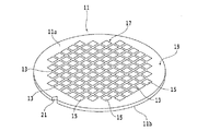
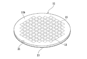
12 研削ユニット
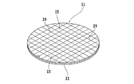
13 ストリート(分割予定ライン)
15 デバイス
18 研削ホイール
23 保護テープ
24 レーザ加工装置
27 改質層
28 レーザビーム照射ユニット
29 分割溝
32 集光器
36 DAF
40 分割装置
Claims (3)
- 複数のデバイスが分割予定ラインによって区画されて表面に形成されたウエーハを個々のデバイスに分割するウエーハの分割方法であって、
ウエーハの表面に保護部材を配設する保護部材配設工程と、
該保護部材配設工程を実施した後、ウエーハの裏面を研削して所定の厚みに加工する裏面研削工程と、
該裏面研削工程を実施した後、ウエーハの裏面からウエーハに対して透過性を有する波長のレーザビームをその集光点を分割予定ラインに対応する内部に位置付けて照射し、デバイスの仕上がり厚さに至らない深さの位置に改質層を形成する改質層形成工程と、
該改質層形成工程を実施した後、ウエーハを該改質層に沿って個々のデバイスに分割するウエーハ分割工程と、
該ウエーハ分割工程を実施した後、個々のデバイスに分割されたウエーハの裏面を研削して該改質層を除去し、該デバイスを仕上がり厚さに形成する改質層除去工程と、
該改質層除去工程を実施した後、ウエーハを収容する開口部を有する環状フレームの該開口部にウエーハを位置づけてダイボンディング用フィルムを介在してウエーハの裏面をダイシングテープに貼着するとともに、該ダイシングテープの外周部を該環状フレームに貼着するフレーム配設工程と、
該フレーム配設工程を実施した後、ウエーハの表面から該保護部材を除去する保護部材除去工程と、
該保護部材除去工程を実施した後、該ダイシングテープを拡張してデバイスとデバイスの間隔を拡張し、該ダイボンディング用フィルムを個々のデバイスに対応して分割するダイボンディング用フィルム分割工程と、
を具備したことを特徴とするウエーハの分割方法。 - 該分割予定ライン上には膜が積層されており、該裏面研削工程を実施する前に、アブレーション加工を施すレーザビームを該分割予定ラインに沿って照射して該膜を切断する膜切断工程を更に具備した請求項1記載のウエーハの分割方法。
- 該膜は、TEGを含む金属膜、Low−k膜を含む絶縁膜、ポリイミド膜を含む樹脂膜の何れかから構成される請求項2記載のウエーハの分割方法。
Priority Applications (2)
| Application Number | Priority Date | Filing Date | Title |
|---|---|---|---|
| JP2010236336A JP5645593B2 (ja) | 2010-10-21 | 2010-10-21 | ウエーハの分割方法 |
| US13/277,874 US8415232B2 (en) | 2010-10-21 | 2011-10-20 | Dividing method for wafer having die bonding film attached to the back side thereof |
Applications Claiming Priority (1)
| Application Number | Priority Date | Filing Date | Title |
|---|---|---|---|
| JP2010236336A JP5645593B2 (ja) | 2010-10-21 | 2010-10-21 | ウエーハの分割方法 |
Publications (2)
| Publication Number | Publication Date |
|---|---|
| JP2012089730A JP2012089730A (ja) | 2012-05-10 |
| JP5645593B2 true JP5645593B2 (ja) | 2014-12-24 |
Family
ID=45973380
Family Applications (1)
| Application Number | Title | Priority Date | Filing Date |
|---|---|---|---|
| JP2010236336A Active JP5645593B2 (ja) | 2010-10-21 | 2010-10-21 | ウエーハの分割方法 |
Country Status (2)
| Country | Link |
|---|---|
| US (1) | US8415232B2 (ja) |
| JP (1) | JP5645593B2 (ja) |
Cited By (1)
| Publication number | Priority date | Publication date | Assignee | Title |
|---|---|---|---|---|
| KR102554988B1 (ko) | 2017-07-24 | 2023-07-12 | 가부시기가이샤 디스코 | 웨이퍼의 가공 방법 |
Families Citing this family (15)
| Publication number | Priority date | Publication date | Assignee | Title |
|---|---|---|---|---|
| JP5939752B2 (ja) * | 2011-09-01 | 2016-06-22 | 株式会社ディスコ | ウェーハの分割方法 |
| JP5964580B2 (ja) * | 2011-12-26 | 2016-08-03 | 株式会社ディスコ | ウェーハの加工方法 |
| JP2014082468A (ja) | 2012-09-25 | 2014-05-08 | Canon Components Inc | 基板部材及びチップの製造方法 |
| US9040389B2 (en) * | 2012-10-09 | 2015-05-26 | Infineon Technologies Ag | Singulation processes |
| DE102015100827A1 (de) | 2015-01-21 | 2016-07-21 | Infineon Technologies Ag | Verfahren zum Bearbeiten eines Halbleitersubstrats und Halbleiterchips |
| JP2016192494A (ja) * | 2015-03-31 | 2016-11-10 | 株式会社ディスコ | ウエーハの分割方法 |
| US9704748B2 (en) * | 2015-06-25 | 2017-07-11 | Infineon Technologies Ag | Method of dicing a wafer |
| JP2017147361A (ja) * | 2016-02-18 | 2017-08-24 | 株式会社ディスコ | ウエーハの加工方法 |
| DE102016211044B4 (de) * | 2016-06-21 | 2024-02-15 | Disco Corporation | Verfahren zum Bearbeiten eines Wafers und Waferbearbeitungssystem |
| DE102017201154A1 (de) | 2017-01-25 | 2018-07-26 | Disco Corporation | Verfahren zum Bearbeiten eines Wafers und Waferbearbeitungssystem |
| JP6781639B2 (ja) * | 2017-01-31 | 2020-11-04 | 株式会社ディスコ | ウエーハ生成方法 |
| DE102017106854A1 (de) * | 2017-03-30 | 2018-10-04 | Infineon Technologies Ag | Trägeranordnung und Verfahren für die Bearbeitung eines Trägers |
| JP6981800B2 (ja) * | 2017-07-28 | 2021-12-17 | 浜松ホトニクス株式会社 | 積層型素子の製造方法 |
| CN108807237A (zh) * | 2018-06-27 | 2018-11-13 | 深圳市矽谷科技有限公司 | 一种固晶工艺结构、固晶机及固晶控制方法 |
| US11538711B2 (en) | 2018-07-23 | 2022-12-27 | Micron Technology, Inc. | Methods for edge trimming of semiconductor wafers and related apparatus |
Family Cites Families (9)
| Publication number | Priority date | Publication date | Assignee | Title |
|---|---|---|---|---|
| JPH1027971A (ja) * | 1996-07-10 | 1998-01-27 | Nec Corp | 有機薄膜多層配線基板の切断方法 |
| JPH1140520A (ja) | 1997-07-23 | 1999-02-12 | Toshiba Corp | ウェーハの分割方法及び半導体装置の製造方法 |
| JP3408805B2 (ja) | 2000-09-13 | 2003-05-19 | 浜松ホトニクス株式会社 | 切断起点領域形成方法及び加工対象物切断方法 |
| JP4109823B2 (ja) | 2000-10-10 | 2008-07-02 | 株式会社東芝 | 半導体装置の製造方法 |
| JP4402974B2 (ja) | 2004-02-09 | 2010-01-20 | 株式会社ディスコ | ウエーハの分割方法 |
| JP2005252196A (ja) * | 2004-03-08 | 2005-09-15 | Toshiba Corp | 半導体装置及びその製造方法 |
| JP4705418B2 (ja) * | 2005-06-29 | 2011-06-22 | 株式会社ディスコ | ウェーハの加工方法 |
| JP2009094127A (ja) * | 2007-10-04 | 2009-04-30 | Furukawa Electric Co Ltd:The | 半導体ウエハ加工用フィルム |
| JP5134928B2 (ja) * | 2007-11-30 | 2013-01-30 | 浜松ホトニクス株式会社 | 加工対象物研削方法 |
-
2010
- 2010-10-21 JP JP2010236336A patent/JP5645593B2/ja active Active
-
2011
- 2011-10-20 US US13/277,874 patent/US8415232B2/en active Active
Cited By (1)
| Publication number | Priority date | Publication date | Assignee | Title |
|---|---|---|---|---|
| KR102554988B1 (ko) | 2017-07-24 | 2023-07-12 | 가부시기가이샤 디스코 | 웨이퍼의 가공 방법 |
Also Published As
| Publication number | Publication date |
|---|---|
| US8415232B2 (en) | 2013-04-09 |
| US20120100694A1 (en) | 2012-04-26 |
| JP2012089730A (ja) | 2012-05-10 |
Similar Documents
| Publication | Publication Date | Title |
|---|---|---|
| JP5645593B2 (ja) | ウエーハの分割方法 | |
| JP6486240B2 (ja) | ウエーハの加工方法 | |
| JP6486239B2 (ja) | ウエーハの加工方法 | |
| JP4847199B2 (ja) | ウエーハに装着された接着フィルムの破断方法 | |
| JP6004705B2 (ja) | 接着フィルム付きチップの形成方法 | |
| JP2009182178A (ja) | デバイスの製造方法 | |
| JP6713212B2 (ja) | 半導体デバイスチップの製造方法 | |
| JP2011108856A (ja) | 光デバイスウエーハの加工方法 | |
| JP2009200140A (ja) | 半導体チップの製造方法 | |
| JP2011003757A (ja) | ウエーハの分割方法 | |
| JP2017092129A (ja) | ウエーハの加工方法 | |
| JP2008235398A (ja) | デバイスの製造方法 | |
| JP6045361B2 (ja) | ウエーハの加工方法 | |
| JP6257365B2 (ja) | ウェーハの加工方法 | |
| JP2017059684A (ja) | ウエーハの加工方法 | |
| JP6029347B2 (ja) | ウエーハの加工方法 | |
| JP2005116739A (ja) | 半導体チップの製造方法 | |
| KR20170029385A (ko) | 웨이퍼 가공 방법 | |
| JP5367450B2 (ja) | 半導体ウエーハの加工方法 | |
| JP2008227276A (ja) | ウエーハの分割方法 | |
| JP5912283B2 (ja) | 粘着テープ及びウエーハの加工方法 | |
| JP2011114018A (ja) | 光デバイスの製造方法 | |
| JP5553586B2 (ja) | ウエーハの加工方法 | |
| JP6576211B2 (ja) | ウエーハの加工方法 | |
| JP6270520B2 (ja) | ウェーハの加工方法 |
Legal Events
| Date | Code | Title | Description |
|---|---|---|---|
| A621 | Written request for application examination |
Free format text: JAPANESE INTERMEDIATE CODE: A621 Effective date: 20130913 |
|
| A131 | Notification of reasons for refusal |
Free format text: JAPANESE INTERMEDIATE CODE: A131 Effective date: 20140722 |
|
| A521 | Request for written amendment filed |
Free format text: JAPANESE INTERMEDIATE CODE: A523 Effective date: 20140917 |
|
| TRDD | Decision of grant or rejection written | ||
| A01 | Written decision to grant a patent or to grant a registration (utility model) |
Free format text: JAPANESE INTERMEDIATE CODE: A01 Effective date: 20141104 |
|
| A61 | First payment of annual fees (during grant procedure) |
Free format text: JAPANESE INTERMEDIATE CODE: A61 Effective date: 20141104 |
|
| R150 | Certificate of patent or registration of utility model |
Ref document number: 5645593 Country of ref document: JP Free format text: JAPANESE INTERMEDIATE CODE: R150 |
|
| R250 | Receipt of annual fees |
Free format text: JAPANESE INTERMEDIATE CODE: R250 |
|
| R250 | Receipt of annual fees |
Free format text: JAPANESE INTERMEDIATE CODE: R250 |
|
| R250 | Receipt of annual fees |
Free format text: JAPANESE INTERMEDIATE CODE: R250 |
|
| R250 | Receipt of annual fees |
Free format text: JAPANESE INTERMEDIATE CODE: R250 |
|
| R250 | Receipt of annual fees |
Free format text: JAPANESE INTERMEDIATE CODE: R250 |
|
| R250 | Receipt of annual fees |
Free format text: JAPANESE INTERMEDIATE CODE: R250 |
|
| R250 | Receipt of annual fees |
Free format text: JAPANESE INTERMEDIATE CODE: R250 |