JP5576885B2 - 補強層を伴う半導体チップ - Google Patents
補強層を伴う半導体チップ Download PDFInfo
- Publication number
- JP5576885B2 JP5576885B2 JP2011550323A JP2011550323A JP5576885B2 JP 5576885 B2 JP5576885 B2 JP 5576885B2 JP 2011550323 A JP2011550323 A JP 2011550323A JP 2011550323 A JP2011550323 A JP 2011550323A JP 5576885 B2 JP5576885 B2 JP 5576885B2
- Authority
- JP
- Japan
- Prior art keywords
- layer
- semiconductor chip
- frame portion
- channel
- forming
- Prior art date
- Legal status (The legal status is an assumption and is not a legal conclusion. Google has not performed a legal analysis and makes no representation as to the accuracy of the status listed.)
- Active
Links
Images


Classifications
-
- H—ELECTRICITY
- H01—ELECTRIC ELEMENTS
- H01L—SEMICONDUCTOR DEVICES NOT COVERED BY CLASS H10
- H01L23/00—Details of semiconductor or other solid state devices
- H01L23/28—Encapsulations, e.g. encapsulating layers, coatings, e.g. for protection
- H01L23/31—Encapsulations, e.g. encapsulating layers, coatings, e.g. for protection characterised by the arrangement or shape
- H01L23/3107—Encapsulations, e.g. encapsulating layers, coatings, e.g. for protection characterised by the arrangement or shape the device being completely enclosed
- H01L23/3142—Sealing arrangements between parts, e.g. adhesion promotors
-
- H—ELECTRICITY
- H01—ELECTRIC ELEMENTS
- H01L—SEMICONDUCTOR DEVICES NOT COVERED BY CLASS H10
- H01L21/00—Processes or apparatus adapted for the manufacture or treatment of semiconductor or solid state devices or of parts thereof
- H01L21/02—Manufacture or treatment of semiconductor devices or of parts thereof
- H01L21/04—Manufacture or treatment of semiconductor devices or of parts thereof the devices having at least one potential-jump barrier or surface barrier, e.g. PN junction, depletion layer or carrier concentration layer
- H01L21/50—Assembly of semiconductor devices using processes or apparatus not provided for in a single one of the subgroups H01L21/06 - H01L21/326, e.g. sealing of a cap to a base of a container
- H01L21/56—Encapsulations, e.g. encapsulation layers, coatings
- H01L21/563—Encapsulation of active face of flip-chip device, e.g. underfilling or underencapsulation of flip-chip, encapsulation preform on chip or mounting substrate
-
- H—ELECTRICITY
- H01—ELECTRIC ELEMENTS
- H01L—SEMICONDUCTOR DEVICES NOT COVERED BY CLASS H10
- H01L23/00—Details of semiconductor or other solid state devices
- H01L23/28—Encapsulations, e.g. encapsulating layers, coatings, e.g. for protection
- H01L23/31—Encapsulations, e.g. encapsulating layers, coatings, e.g. for protection characterised by the arrangement or shape
- H01L23/3157—Partial encapsulation or coating
- H01L23/3171—Partial encapsulation or coating the coating being directly applied to the semiconductor body, e.g. passivation layer
-
- H—ELECTRICITY
- H01—ELECTRIC ELEMENTS
- H01L—SEMICONDUCTOR DEVICES NOT COVERED BY CLASS H10
- H01L24/00—Arrangements for connecting or disconnecting semiconductor or solid-state bodies; Methods or apparatus related thereto
- H01L24/01—Means for bonding being attached to, or being formed on, the surface to be connected, e.g. chip-to-package, die-attach, "first-level" interconnects; Manufacturing methods related thereto
- H01L24/02—Bonding areas ; Manufacturing methods related thereto
- H01L24/04—Structure, shape, material or disposition of the bonding areas prior to the connecting process
- H01L24/05—Structure, shape, material or disposition of the bonding areas prior to the connecting process of an individual bonding area
-
- H—ELECTRICITY
- H01—ELECTRIC ELEMENTS
- H01L—SEMICONDUCTOR DEVICES NOT COVERED BY CLASS H10
- H01L2224/00—Indexing scheme for arrangements for connecting or disconnecting semiconductor or solid-state bodies and methods related thereto as covered by H01L24/00
- H01L2224/01—Means for bonding being attached to, or being formed on, the surface to be connected, e.g. chip-to-package, die-attach, "first-level" interconnects; Manufacturing methods related thereto
- H01L2224/02—Bonding areas; Manufacturing methods related thereto
- H01L2224/04—Structure, shape, material or disposition of the bonding areas prior to the connecting process
- H01L2224/0401—Bonding areas specifically adapted for bump connectors, e.g. under bump metallisation [UBM]
-
- H—ELECTRICITY
- H01—ELECTRIC ELEMENTS
- H01L—SEMICONDUCTOR DEVICES NOT COVERED BY CLASS H10
- H01L2224/00—Indexing scheme for arrangements for connecting or disconnecting semiconductor or solid-state bodies and methods related thereto as covered by H01L24/00
- H01L2224/01—Means for bonding being attached to, or being formed on, the surface to be connected, e.g. chip-to-package, die-attach, "first-level" interconnects; Manufacturing methods related thereto
- H01L2224/02—Bonding areas; Manufacturing methods related thereto
- H01L2224/04—Structure, shape, material or disposition of the bonding areas prior to the connecting process
- H01L2224/05—Structure, shape, material or disposition of the bonding areas prior to the connecting process of an individual bonding area
- H01L2224/05001—Internal layers
- H01L2224/0502—Disposition
- H01L2224/05022—Disposition the internal layer being at least partially embedded in the surface
-
- H—ELECTRICITY
- H01—ELECTRIC ELEMENTS
- H01L—SEMICONDUCTOR DEVICES NOT COVERED BY CLASS H10
- H01L2224/00—Indexing scheme for arrangements for connecting or disconnecting semiconductor or solid-state bodies and methods related thereto as covered by H01L24/00
- H01L2224/01—Means for bonding being attached to, or being formed on, the surface to be connected, e.g. chip-to-package, die-attach, "first-level" interconnects; Manufacturing methods related thereto
- H01L2224/02—Bonding areas; Manufacturing methods related thereto
- H01L2224/04—Structure, shape, material or disposition of the bonding areas prior to the connecting process
- H01L2224/05—Structure, shape, material or disposition of the bonding areas prior to the connecting process of an individual bonding area
- H01L2224/05001—Internal layers
- H01L2224/05099—Material
- H01L2224/051—Material with a principal constituent of the material being a metal or a metalloid, e.g. boron [B], silicon [Si], germanium [Ge], arsenic [As], antimony [Sb], tellurium [Te] and polonium [Po], and alloys thereof
- H01L2224/05138—Material with a principal constituent of the material being a metal or a metalloid, e.g. boron [B], silicon [Si], germanium [Ge], arsenic [As], antimony [Sb], tellurium [Te] and polonium [Po], and alloys thereof the principal constituent melting at a temperature of greater than or equal to 950°C and less than 1550°C
- H01L2224/05139—Silver [Ag] as principal constituent
-
- H—ELECTRICITY
- H01—ELECTRIC ELEMENTS
- H01L—SEMICONDUCTOR DEVICES NOT COVERED BY CLASS H10
- H01L2224/00—Indexing scheme for arrangements for connecting or disconnecting semiconductor or solid-state bodies and methods related thereto as covered by H01L24/00
- H01L2224/01—Means for bonding being attached to, or being formed on, the surface to be connected, e.g. chip-to-package, die-attach, "first-level" interconnects; Manufacturing methods related thereto
- H01L2224/02—Bonding areas; Manufacturing methods related thereto
- H01L2224/04—Structure, shape, material or disposition of the bonding areas prior to the connecting process
- H01L2224/05—Structure, shape, material or disposition of the bonding areas prior to the connecting process of an individual bonding area
- H01L2224/05001—Internal layers
- H01L2224/05099—Material
- H01L2224/051—Material with a principal constituent of the material being a metal or a metalloid, e.g. boron [B], silicon [Si], germanium [Ge], arsenic [As], antimony [Sb], tellurium [Te] and polonium [Po], and alloys thereof
- H01L2224/05138—Material with a principal constituent of the material being a metal or a metalloid, e.g. boron [B], silicon [Si], germanium [Ge], arsenic [As], antimony [Sb], tellurium [Te] and polonium [Po], and alloys thereof the principal constituent melting at a temperature of greater than or equal to 950°C and less than 1550°C
- H01L2224/05144—Gold [Au] as principal constituent
-
- H—ELECTRICITY
- H01—ELECTRIC ELEMENTS
- H01L—SEMICONDUCTOR DEVICES NOT COVERED BY CLASS H10
- H01L2224/00—Indexing scheme for arrangements for connecting or disconnecting semiconductor or solid-state bodies and methods related thereto as covered by H01L24/00
- H01L2224/01—Means for bonding being attached to, or being formed on, the surface to be connected, e.g. chip-to-package, die-attach, "first-level" interconnects; Manufacturing methods related thereto
- H01L2224/02—Bonding areas; Manufacturing methods related thereto
- H01L2224/04—Structure, shape, material or disposition of the bonding areas prior to the connecting process
- H01L2224/05—Structure, shape, material or disposition of the bonding areas prior to the connecting process of an individual bonding area
- H01L2224/05001—Internal layers
- H01L2224/05099—Material
- H01L2224/051—Material with a principal constituent of the material being a metal or a metalloid, e.g. boron [B], silicon [Si], germanium [Ge], arsenic [As], antimony [Sb], tellurium [Te] and polonium [Po], and alloys thereof
- H01L2224/05138—Material with a principal constituent of the material being a metal or a metalloid, e.g. boron [B], silicon [Si], germanium [Ge], arsenic [As], antimony [Sb], tellurium [Te] and polonium [Po], and alloys thereof the principal constituent melting at a temperature of greater than or equal to 950°C and less than 1550°C
- H01L2224/05147—Copper [Cu] as principal constituent
-
- H—ELECTRICITY
- H01—ELECTRIC ELEMENTS
- H01L—SEMICONDUCTOR DEVICES NOT COVERED BY CLASS H10
- H01L2224/00—Indexing scheme for arrangements for connecting or disconnecting semiconductor or solid-state bodies and methods related thereto as covered by H01L24/00
- H01L2224/01—Means for bonding being attached to, or being formed on, the surface to be connected, e.g. chip-to-package, die-attach, "first-level" interconnects; Manufacturing methods related thereto
- H01L2224/02—Bonding areas; Manufacturing methods related thereto
- H01L2224/04—Structure, shape, material or disposition of the bonding areas prior to the connecting process
- H01L2224/05—Structure, shape, material or disposition of the bonding areas prior to the connecting process of an individual bonding area
- H01L2224/05001—Internal layers
- H01L2224/05099—Material
- H01L2224/051—Material with a principal constituent of the material being a metal or a metalloid, e.g. boron [B], silicon [Si], germanium [Ge], arsenic [As], antimony [Sb], tellurium [Te] and polonium [Po], and alloys thereof
- H01L2224/05163—Material with a principal constituent of the material being a metal or a metalloid, e.g. boron [B], silicon [Si], germanium [Ge], arsenic [As], antimony [Sb], tellurium [Te] and polonium [Po], and alloys thereof the principal constituent melting at a temperature of greater than 1550°C
- H01L2224/05171—Chromium [Cr] as principal constituent
-
- H—ELECTRICITY
- H01—ELECTRIC ELEMENTS
- H01L—SEMICONDUCTOR DEVICES NOT COVERED BY CLASS H10
- H01L2224/00—Indexing scheme for arrangements for connecting or disconnecting semiconductor or solid-state bodies and methods related thereto as covered by H01L24/00
- H01L2224/01—Means for bonding being attached to, or being formed on, the surface to be connected, e.g. chip-to-package, die-attach, "first-level" interconnects; Manufacturing methods related thereto
- H01L2224/02—Bonding areas; Manufacturing methods related thereto
- H01L2224/04—Structure, shape, material or disposition of the bonding areas prior to the connecting process
- H01L2224/05—Structure, shape, material or disposition of the bonding areas prior to the connecting process of an individual bonding area
- H01L2224/0554—External layer
- H01L2224/0556—Disposition
- H01L2224/05571—Disposition the external layer being disposed in a recess of the surface
- H01L2224/05572—Disposition the external layer being disposed in a recess of the surface the external layer extending out of an opening
-
- H—ELECTRICITY
- H01—ELECTRIC ELEMENTS
- H01L—SEMICONDUCTOR DEVICES NOT COVERED BY CLASS H10
- H01L2224/00—Indexing scheme for arrangements for connecting or disconnecting semiconductor or solid-state bodies and methods related thereto as covered by H01L24/00
- H01L2224/01—Means for bonding being attached to, or being formed on, the surface to be connected, e.g. chip-to-package, die-attach, "first-level" interconnects; Manufacturing methods related thereto
- H01L2224/02—Bonding areas; Manufacturing methods related thereto
- H01L2224/04—Structure, shape, material or disposition of the bonding areas prior to the connecting process
- H01L2224/05—Structure, shape, material or disposition of the bonding areas prior to the connecting process of an individual bonding area
- H01L2224/0554—External layer
- H01L2224/05599—Material
- H01L2224/056—Material with a principal constituent of the material being a metal or a metalloid, e.g. boron [B], silicon [Si], germanium [Ge], arsenic [As], antimony [Sb], tellurium [Te] and polonium [Po], and alloys thereof
- H01L2224/05638—Material with a principal constituent of the material being a metal or a metalloid, e.g. boron [B], silicon [Si], germanium [Ge], arsenic [As], antimony [Sb], tellurium [Te] and polonium [Po], and alloys thereof the principal constituent melting at a temperature of greater than or equal to 950°C and less than 1550°C
- H01L2224/05639—Silver [Ag] as principal constituent
-
- H—ELECTRICITY
- H01—ELECTRIC ELEMENTS
- H01L—SEMICONDUCTOR DEVICES NOT COVERED BY CLASS H10
- H01L2224/00—Indexing scheme for arrangements for connecting or disconnecting semiconductor or solid-state bodies and methods related thereto as covered by H01L24/00
- H01L2224/01—Means for bonding being attached to, or being formed on, the surface to be connected, e.g. chip-to-package, die-attach, "first-level" interconnects; Manufacturing methods related thereto
- H01L2224/02—Bonding areas; Manufacturing methods related thereto
- H01L2224/04—Structure, shape, material or disposition of the bonding areas prior to the connecting process
- H01L2224/05—Structure, shape, material or disposition of the bonding areas prior to the connecting process of an individual bonding area
- H01L2224/0554—External layer
- H01L2224/05599—Material
- H01L2224/056—Material with a principal constituent of the material being a metal or a metalloid, e.g. boron [B], silicon [Si], germanium [Ge], arsenic [As], antimony [Sb], tellurium [Te] and polonium [Po], and alloys thereof
- H01L2224/05638—Material with a principal constituent of the material being a metal or a metalloid, e.g. boron [B], silicon [Si], germanium [Ge], arsenic [As], antimony [Sb], tellurium [Te] and polonium [Po], and alloys thereof the principal constituent melting at a temperature of greater than or equal to 950°C and less than 1550°C
- H01L2224/05644—Gold [Au] as principal constituent
-
- H—ELECTRICITY
- H01—ELECTRIC ELEMENTS
- H01L—SEMICONDUCTOR DEVICES NOT COVERED BY CLASS H10
- H01L2224/00—Indexing scheme for arrangements for connecting or disconnecting semiconductor or solid-state bodies and methods related thereto as covered by H01L24/00
- H01L2224/01—Means for bonding being attached to, or being formed on, the surface to be connected, e.g. chip-to-package, die-attach, "first-level" interconnects; Manufacturing methods related thereto
- H01L2224/02—Bonding areas; Manufacturing methods related thereto
- H01L2224/04—Structure, shape, material or disposition of the bonding areas prior to the connecting process
- H01L2224/05—Structure, shape, material or disposition of the bonding areas prior to the connecting process of an individual bonding area
- H01L2224/0554—External layer
- H01L2224/05599—Material
- H01L2224/056—Material with a principal constituent of the material being a metal or a metalloid, e.g. boron [B], silicon [Si], germanium [Ge], arsenic [As], antimony [Sb], tellurium [Te] and polonium [Po], and alloys thereof
- H01L2224/05638—Material with a principal constituent of the material being a metal or a metalloid, e.g. boron [B], silicon [Si], germanium [Ge], arsenic [As], antimony [Sb], tellurium [Te] and polonium [Po], and alloys thereof the principal constituent melting at a temperature of greater than or equal to 950°C and less than 1550°C
- H01L2224/05647—Copper [Cu] as principal constituent
-
- H—ELECTRICITY
- H01—ELECTRIC ELEMENTS
- H01L—SEMICONDUCTOR DEVICES NOT COVERED BY CLASS H10
- H01L2224/00—Indexing scheme for arrangements for connecting or disconnecting semiconductor or solid-state bodies and methods related thereto as covered by H01L24/00
- H01L2224/01—Means for bonding being attached to, or being formed on, the surface to be connected, e.g. chip-to-package, die-attach, "first-level" interconnects; Manufacturing methods related thereto
- H01L2224/02—Bonding areas; Manufacturing methods related thereto
- H01L2224/04—Structure, shape, material or disposition of the bonding areas prior to the connecting process
- H01L2224/05—Structure, shape, material or disposition of the bonding areas prior to the connecting process of an individual bonding area
- H01L2224/0554—External layer
- H01L2224/05599—Material
- H01L2224/056—Material with a principal constituent of the material being a metal or a metalloid, e.g. boron [B], silicon [Si], germanium [Ge], arsenic [As], antimony [Sb], tellurium [Te] and polonium [Po], and alloys thereof
- H01L2224/05638—Material with a principal constituent of the material being a metal or a metalloid, e.g. boron [B], silicon [Si], germanium [Ge], arsenic [As], antimony [Sb], tellurium [Te] and polonium [Po], and alloys thereof the principal constituent melting at a temperature of greater than or equal to 950°C and less than 1550°C
- H01L2224/05655—Nickel [Ni] as principal constituent
-
- H—ELECTRICITY
- H01—ELECTRIC ELEMENTS
- H01L—SEMICONDUCTOR DEVICES NOT COVERED BY CLASS H10
- H01L2224/00—Indexing scheme for arrangements for connecting or disconnecting semiconductor or solid-state bodies and methods related thereto as covered by H01L24/00
- H01L2224/01—Means for bonding being attached to, or being formed on, the surface to be connected, e.g. chip-to-package, die-attach, "first-level" interconnects; Manufacturing methods related thereto
- H01L2224/10—Bump connectors; Manufacturing methods related thereto
- H01L2224/15—Structure, shape, material or disposition of the bump connectors after the connecting process
- H01L2224/16—Structure, shape, material or disposition of the bump connectors after the connecting process of an individual bump connector
- H01L2224/161—Disposition
- H01L2224/16151—Disposition the bump connector connecting between a semiconductor or solid-state body and an item not being a semiconductor or solid-state body, e.g. chip-to-substrate, chip-to-passive
- H01L2224/16221—Disposition the bump connector connecting between a semiconductor or solid-state body and an item not being a semiconductor or solid-state body, e.g. chip-to-substrate, chip-to-passive the body and the item being stacked
- H01L2224/16225—Disposition the bump connector connecting between a semiconductor or solid-state body and an item not being a semiconductor or solid-state body, e.g. chip-to-substrate, chip-to-passive the body and the item being stacked the item being non-metallic, e.g. insulating substrate with or without metallisation
-
- H—ELECTRICITY
- H01—ELECTRIC ELEMENTS
- H01L—SEMICONDUCTOR DEVICES NOT COVERED BY CLASS H10
- H01L2224/00—Indexing scheme for arrangements for connecting or disconnecting semiconductor or solid-state bodies and methods related thereto as covered by H01L24/00
- H01L2224/01—Means for bonding being attached to, or being formed on, the surface to be connected, e.g. chip-to-package, die-attach, "first-level" interconnects; Manufacturing methods related thereto
- H01L2224/26—Layer connectors, e.g. plate connectors, solder or adhesive layers; Manufacturing methods related thereto
- H01L2224/31—Structure, shape, material or disposition of the layer connectors after the connecting process
- H01L2224/32—Structure, shape, material or disposition of the layer connectors after the connecting process of an individual layer connector
- H01L2224/321—Disposition
- H01L2224/32151—Disposition the layer connector connecting between a semiconductor or solid-state body and an item not being a semiconductor or solid-state body, e.g. chip-to-substrate, chip-to-passive
- H01L2224/32221—Disposition the layer connector connecting between a semiconductor or solid-state body and an item not being a semiconductor or solid-state body, e.g. chip-to-substrate, chip-to-passive the body and the item being stacked
- H01L2224/32225—Disposition the layer connector connecting between a semiconductor or solid-state body and an item not being a semiconductor or solid-state body, e.g. chip-to-substrate, chip-to-passive the body and the item being stacked the item being non-metallic, e.g. insulating substrate with or without metallisation
-
- H—ELECTRICITY
- H01—ELECTRIC ELEMENTS
- H01L—SEMICONDUCTOR DEVICES NOT COVERED BY CLASS H10
- H01L2224/00—Indexing scheme for arrangements for connecting or disconnecting semiconductor or solid-state bodies and methods related thereto as covered by H01L24/00
- H01L2224/73—Means for bonding being of different types provided for in two or more of groups H01L2224/10, H01L2224/18, H01L2224/26, H01L2224/34, H01L2224/42, H01L2224/50, H01L2224/63, H01L2224/71
- H01L2224/732—Location after the connecting process
- H01L2224/73201—Location after the connecting process on the same surface
- H01L2224/73203—Bump and layer connectors
- H01L2224/73204—Bump and layer connectors the bump connector being embedded into the layer connector
-
- H—ELECTRICITY
- H01—ELECTRIC ELEMENTS
- H01L—SEMICONDUCTOR DEVICES NOT COVERED BY CLASS H10
- H01L2924/00—Indexing scheme for arrangements or methods for connecting or disconnecting semiconductor or solid-state bodies as covered by H01L24/00
- H01L2924/01—Chemical elements
- H01L2924/01046—Palladium [Pd]
-
- H—ELECTRICITY
- H01—ELECTRIC ELEMENTS
- H01L—SEMICONDUCTOR DEVICES NOT COVERED BY CLASS H10
- H01L2924/00—Indexing scheme for arrangements or methods for connecting or disconnecting semiconductor or solid-state bodies as covered by H01L24/00
- H01L2924/01—Chemical elements
- H01L2924/01078—Platinum [Pt]
-
- H—ELECTRICITY
- H01—ELECTRIC ELEMENTS
- H01L—SEMICONDUCTOR DEVICES NOT COVERED BY CLASS H10
- H01L2924/00—Indexing scheme for arrangements or methods for connecting or disconnecting semiconductor or solid-state bodies as covered by H01L24/00
- H01L2924/01—Chemical elements
- H01L2924/01079—Gold [Au]
-
- H—ELECTRICITY
- H01—ELECTRIC ELEMENTS
- H01L—SEMICONDUCTOR DEVICES NOT COVERED BY CLASS H10
- H01L2924/00—Indexing scheme for arrangements or methods for connecting or disconnecting semiconductor or solid-state bodies as covered by H01L24/00
- H01L2924/013—Alloys
- H01L2924/0132—Binary Alloys
- H01L2924/01322—Eutectic Alloys, i.e. obtained by a liquid transforming into two solid phases
-
- H—ELECTRICITY
- H01—ELECTRIC ELEMENTS
- H01L—SEMICONDUCTOR DEVICES NOT COVERED BY CLASS H10
- H01L2924/00—Indexing scheme for arrangements or methods for connecting or disconnecting semiconductor or solid-state bodies as covered by H01L24/00
- H01L2924/10—Details of semiconductor or other solid state devices to be connected
- H01L2924/11—Device type
- H01L2924/12—Passive devices, e.g. 2 terminal devices
- H01L2924/1204—Optical Diode
- H01L2924/12044—OLED
-
- H—ELECTRICITY
- H01—ELECTRIC ELEMENTS
- H01L—SEMICONDUCTOR DEVICES NOT COVERED BY CLASS H10
- H01L2924/00—Indexing scheme for arrangements or methods for connecting or disconnecting semiconductor or solid-state bodies as covered by H01L24/00
- H01L2924/19—Details of hybrid assemblies other than the semiconductor or other solid state devices to be connected
- H01L2924/1901—Structure
- H01L2924/1904—Component type
- H01L2924/19041—Component type being a capacitor
Description
Claims (21)
- 不動態化層(55)を有する半導体チップ(15)を提供することと、
中央部分(65)及び前記中央部分から空間的に分離される第1のフレーム部分(70)を伴うポリマ層(60)を前記不動態化層(55)上に形成して、前記不動態化層(55)にまで延びてはいるが前記不動態化層(55)を貫通してはいない第1のチャネル(80)を画定することとを備えた製造の方法。 - 複数の半田構造(90)を前記中央部分(65)に結合することを備えた請求項1の方法。
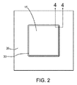
- 長方形設置面を伴う前記第1のフレーム部分(70)を形成することを備えた請求項1の方法。
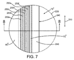
- 蛇行設置面を伴う前記第1のチャネル(80’)を画定する前記第1のフレーム部分(70)を形成することを備えた請求項1の方法。
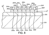
- 前記半導体チップ(15”)の前記不動態化層(55)から外側に向く前記第1のフレーム部分(75”)の表面内に溝(250a)を形成することを備えた請求項1の方法。
- 前記溝(250a)は前記第1のフレーム部分(75”)の周囲にわたって延在する請求項5の方法。
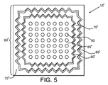
- 前記第1のフレーム部分(70)からから空間的に分離される第2のフレーム部分(75)を伴う前記ポリマ層(60)を形成して第2のチャネル(85)を画定することを備えた請求項1の方法。
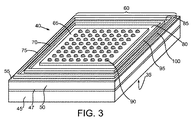
- 中央部分(65)及び前記中央部分から空間的に分離される第1のフレーム部分(70)を有するポリマ層(60)を半導体チップ(15)の不動態化層(55)上に形成して、前記不動態化層(55)にまで延びてはいるが前記不動態化層(55)を貫通してはいない第1のチャネル(80)を画定することと、
前記不動態化層(55)が基板(20)に対向するが接合部領域を残して前記基板(20)からは分離されている状態で前記半導体チップ(15)を前記基板(20)に結合することと、
前記接合部領域内に下層充填(30)を配置することとを備えた製造の方法であって、
前記下層充填の一部分が前記チャネル(80)内に侵入して前記ポリマ層(60)と前記下層充填(30)の間の機械的な結合を確立する製造の方法。 - 前記半導体チップ(15)と前記基板(20)の間に複数の相互接続(105,110)を形成することを備えた請求項8の方法。
- 前記相互接続は半田接合を備えている請求項9の方法。
- 長方形設置面を伴う前記第1のフレーム部分(70)を形成することを備えた請求項8の方法。
- 前記第1のフレーム部分を形成して長方形の設置面を伴う前記第1のチャネル(80)を画定することを備えた請求項11の方法。
- 前記第1のフレーム部分を形成して蛇行設置面を伴う前記第1のチャネル(80’)を画定することを備えた請求項8の方法。
- 前記半導体チップ(15”)の前記不動態化層(55)から外側に向く前記第1のフレーム部分(75”)の表面内に溝(250a)を形成することを備えた請求項8の方法。
- 前記溝(250a)は前記第1のフレーム部分の周囲にわたって延在する請求項14の方法。
- 前記第1のフレーム部分からから空間的に分離される第2のフレーム部分を伴う前記ポリマ層を形成して第2のチャネルを画定することを備えた請求項8の方法。
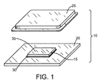
- 不動態化層(55)を有する半導体チップ(15)と、前記不動態化層(55)上のポリマ層(60)とを備えた装置であって、
前記ポリマ層(60)は前記不動態化層(55)にまで延びてはいるが前記不動態化層(55)を貫通してはいない第1のチャネル(80)を画定するために中央部分(65)と前記中央部分(65)から空間的に分離される第1のフレーム部分(70)とを有している装置。 - 前記中央部分に結合される複数の半田構造(115)を備えた請求項17の装置。
- 前記第1のフレーム部分(70)は長方形の設置面を備えている請求項17の装置。
- 前記第1のチャネル(80)は長方形の設置面を備えている請求項19の装置。
- 前記第1のチャネル(80’)は蛇行設置面を備えている請求項17の装置。
Applications Claiming Priority (3)
| Application Number | Priority Date | Filing Date | Title |
|---|---|---|---|
| US12/388,092 | 2009-02-18 | ||
| US12/388,092 US7897433B2 (en) | 2009-02-18 | 2009-02-18 | Semiconductor chip with reinforcement layer and method of making the same |
| PCT/US2010/024462 WO2010096473A2 (en) | 2009-02-18 | 2010-02-17 | Semiconductor chip with reinforcement layer |
Publications (3)
| Publication Number | Publication Date |
|---|---|
| JP2012518282A JP2012518282A (ja) | 2012-08-09 |
| JP2012518282A5 JP2012518282A5 (ja) | 2013-04-04 |
| JP5576885B2 true JP5576885B2 (ja) | 2014-08-20 |
Family
ID=42224974
Family Applications (1)
| Application Number | Title | Priority Date | Filing Date |
|---|---|---|---|
| JP2011550323A Active JP5576885B2 (ja) | 2009-02-18 | 2010-02-17 | 補強層を伴う半導体チップ |
Country Status (7)
| Country | Link |
|---|---|
| US (1) | US7897433B2 (ja) |
| EP (1) | EP2399284B1 (ja) |
| JP (1) | JP5576885B2 (ja) |
| KR (1) | KR101308100B1 (ja) |
| CN (1) | CN102318051B (ja) |
| SG (1) | SG173447A1 (ja) |
| WO (1) | WO2010096473A2 (ja) |
Families Citing this family (13)
| Publication number | Priority date | Publication date | Assignee | Title |
|---|---|---|---|---|
| US8058108B2 (en) | 2010-03-10 | 2011-11-15 | Ati Technologies Ulc | Methods of forming semiconductor chip underfill anchors |
| US8476115B2 (en) | 2011-05-03 | 2013-07-02 | Stats Chippac, Ltd. | Semiconductor device and method of mounting cover to semiconductor die and interposer with adhesive material |
| US8624404B1 (en) | 2012-06-25 | 2014-01-07 | Advanced Micro Devices, Inc. | Integrated circuit package having offset vias |
| US8937009B2 (en) | 2013-04-25 | 2015-01-20 | International Business Machines Corporation | Far back end of the line metallization method and structures |
| TWI467711B (zh) * | 2013-09-10 | 2015-01-01 | Chipbond Technology Corp | 半導體結構 |
| US9466547B1 (en) | 2015-06-09 | 2016-10-11 | Globalfoundries Inc. | Passivation layer topography |
| US9779940B2 (en) * | 2015-07-01 | 2017-10-03 | Zhuahai Advanced Chip Carriers & Electronic Substrate Solutions Technologies Co. Ltd. | Chip package |
| US9589920B2 (en) * | 2015-07-01 | 2017-03-07 | Zhuhai Advanced Chip Carriers & Electronic Substrate Solutions Technologies Co. Ltd. | Chip package |
| US20200251683A1 (en) * | 2019-01-31 | 2020-08-06 | Wuhan China Star Optoelectronics Semiconductor Display Technology Co., Ltd. | Organic light emitting diode display panel and preparation method thereof |
| EP3800660A1 (en) * | 2019-10-02 | 2021-04-07 | STMicroelectronics S.r.l. | Silicon carbide power device with improved robustness and corresponding manufacturing process |
| US20210305158A1 (en) * | 2020-03-27 | 2021-09-30 | Intel Corporation | Novel wlcsp reliability improvement for package edges including package shielding |
| KR20220006929A (ko) | 2020-07-09 | 2022-01-18 | 삼성전자주식회사 | 반도체 패키지 |
| JP2022043997A (ja) | 2020-09-04 | 2022-03-16 | エスティーマイクロエレクトロニクス エス.アール.エル. | 信頼性を改善した電子装置の要素の製造方法、及び関連要素、電子装置、及び電子機器 |
Family Cites Families (27)
| Publication number | Priority date | Publication date | Assignee | Title |
|---|---|---|---|---|
| JPH03133161A (ja) * | 1989-10-19 | 1991-06-06 | Toshiba Corp | 半導体装置 |
| US5861658A (en) | 1996-10-03 | 1999-01-19 | International Business Machines Corporation | Inorganic seal for encapsulation of an organic layer and method for making the same |
| US6022791A (en) * | 1997-10-15 | 2000-02-08 | International Business Machines Corporation | Chip crack stop |
| US6324069B1 (en) | 1997-10-29 | 2001-11-27 | Hestia Technologies, Inc. | Chip package with molded underfill |
| US6049124A (en) | 1997-12-10 | 2000-04-11 | Intel Corporation | Semiconductor package |
| JP2000269386A (ja) | 1999-03-15 | 2000-09-29 | Texas Instr Japan Ltd | 半導体装置 |
| JP3521383B2 (ja) * | 1999-04-28 | 2004-04-19 | 新光電気工業株式会社 | 半導体装置及びその製造方法 |
| US6122171A (en) | 1999-07-30 | 2000-09-19 | Micron Technology, Inc. | Heat sink chip package and method of making |
| US7267148B2 (en) * | 1999-08-10 | 2007-09-11 | Michelin Recherche Et Technique S.A. | Measurement of adherence between a vehicle wheel and the roadway |
| JP2002270735A (ja) | 2001-03-13 | 2002-09-20 | Nec Corp | 半導体装置及びその製造方法 |
| JP4088120B2 (ja) | 2002-08-12 | 2008-05-21 | 株式会社ルネサステクノロジ | 半導体装置 |
| JP2004200532A (ja) * | 2002-12-20 | 2004-07-15 | Renesas Technology Corp | 半導体装置およびその製造方法 |
| JP4346333B2 (ja) | 2003-03-26 | 2009-10-21 | 新光電気工業株式会社 | 半導体素子を内蔵した多層回路基板の製造方法 |
| US7223673B2 (en) * | 2004-07-15 | 2007-05-29 | Taiwan Semiconductor Manufacturing Company, Ltd. | Method of manufacturing semiconductor device with crack prevention ring |
| JP2006041239A (ja) * | 2004-07-28 | 2006-02-09 | Toshiba Corp | 配線基板及び磁気ディスク装置 |
| DE102005003390B4 (de) | 2005-01-24 | 2007-09-13 | Qimonda Ag | Substrat für ein FBGA-Halbleiterbauelement |
| JP4675147B2 (ja) * | 2005-05-10 | 2011-04-20 | パナソニック株式会社 | 半導体装置 |
| US20060278957A1 (en) | 2005-06-09 | 2006-12-14 | Zong-Huei Lin | Fabrication of semiconductor integrated circuit chips |
| CN100461408C (zh) | 2005-09-28 | 2009-02-11 | 中芯国际集成电路制造(上海)有限公司 | 带有密封环拐角结构的集成电路器件 |
| TWI275187B (en) * | 2005-11-30 | 2007-03-01 | Advanced Semiconductor Eng | Flip chip package and manufacturing method of the same |
| JP5118300B2 (ja) | 2005-12-20 | 2013-01-16 | 富士通セミコンダクター株式会社 | 半導体装置及びその製造方法 |
| JP2008078382A (ja) | 2006-09-21 | 2008-04-03 | Toshiba Corp | 半導体装置とその製造方法 |
| US8736039B2 (en) | 2006-10-06 | 2014-05-27 | Taiwan Semiconductor Manufacturing Co., Ltd. | Stacked structures and methods of forming stacked structures |
| US20080169555A1 (en) | 2007-01-16 | 2008-07-17 | Ati Technologies Ulc | Anchor structure for an integrated circuit |
| US7732932B2 (en) | 2007-08-03 | 2010-06-08 | International Business Machines Corporation | Semiconductor chips with crack stop regions for reducing crack propagation from chip edges/corners |
| KR100910233B1 (ko) | 2008-01-02 | 2009-07-31 | 주식회사 하이닉스반도체 | 적층 웨이퍼 레벨 패키지 |
| US8441804B2 (en) | 2008-07-25 | 2013-05-14 | Infineon Technologies Ag | Semiconductor device and method of manufacturing a semiconductor device |
-
2009
- 2009-02-18 US US12/388,092 patent/US7897433B2/en active Active
-
2010
- 2010-02-17 WO PCT/US2010/024462 patent/WO2010096473A2/en active Application Filing
- 2010-02-17 KR KR1020117021554A patent/KR101308100B1/ko active IP Right Grant
- 2010-02-17 JP JP2011550323A patent/JP5576885B2/ja active Active
- 2010-02-17 EP EP10704716.9A patent/EP2399284B1/en not_active Not-in-force
- 2010-02-17 SG SG2011053386A patent/SG173447A1/en unknown
- 2010-02-17 CN CN201080008014.8A patent/CN102318051B/zh active Active
Also Published As
| Publication number | Publication date |
|---|---|
| KR20110126707A (ko) | 2011-11-23 |
| WO2010096473A2 (en) | 2010-08-26 |
| KR101308100B1 (ko) | 2013-09-12 |
| CN102318051A (zh) | 2012-01-11 |
| WO2010096473A3 (en) | 2011-02-03 |
| SG173447A1 (en) | 2011-09-29 |
| EP2399284B1 (en) | 2015-06-17 |
| EP2399284A2 (en) | 2011-12-28 |
| JP2012518282A (ja) | 2012-08-09 |
| CN102318051B (zh) | 2014-02-26 |
| US20100207281A1 (en) | 2010-08-19 |
| US7897433B2 (en) | 2011-03-01 |
Similar Documents
| Publication | Publication Date | Title |
|---|---|---|
| JP5576885B2 (ja) | 補強層を伴う半導体チップ | |
| US11916023B2 (en) | Thermal interface material having different thicknesses in packages | |
| US11069539B2 (en) | 3D packages and methods for forming the same | |
| KR101903903B1 (ko) | 감소된 두께를 갖는 디바이스 패키지 및 그 형성 방법 | |
| TWI765520B (zh) | 半導體封裝以及其製造方法 | |
| US20200035647A1 (en) | Stacked Integrated Circuit Structure and Method of Forming | |
| KR102108236B1 (ko) | 반도체 패키지들 내의 금속화 패턴들 및 그 형성 방법들 | |
| KR101643471B1 (ko) | 리세싱된 엣지들을 갖는 반도체 디바이스 및 그 제조방법 | |
| CN110957229B (zh) | 半导体器件和形成半导体器件的方法 | |
| TWI650807B (zh) | 封裝體及其形成方法 | |
| US20140264933A1 (en) | Wafer Level Chip Scale Packaging Intermediate Structure Apparatus and Method | |
| US9903024B2 (en) | Substrate having electrical interconnection structures and fabrication method thereof | |
| TW201724357A (zh) | 整合扇出結構及其形成方法 | |
| KR102061342B1 (ko) | 강화된 범프 체결 구조를 포함하는 전자 소자의 패키지 및 제조 방법 | |
| JP2013131652A (ja) | 半導体装置の製造方法、半導体ウェハの加工方法、半導体ウェハ | |
| TW201701431A (zh) | 半導體裝置及其製造方法 | |
| JP2002025948A (ja) | ウエハーの分割方法、半導体デバイス、および半導体デバイスの製造方法 | |
| TW202027245A (zh) | 半導體封裝體 | |
| US20230260899A1 (en) | Semiconductor package and manufacturing method thereof | |
| KR101013545B1 (ko) | 스택 패키지 및 그의 제조방법 | |
| US11404394B2 (en) | Chip package structure with integrated device integrated beneath the semiconductor chip |
Legal Events
| Date | Code | Title | Description |
|---|---|---|---|
| A521 | Request for written amendment filed |
Free format text: JAPANESE INTERMEDIATE CODE: A523 Effective date: 20130215 |
|
| A621 | Written request for application examination |
Free format text: JAPANESE INTERMEDIATE CODE: A621 Effective date: 20130215 |
|
| A977 | Report on retrieval |
Free format text: JAPANESE INTERMEDIATE CODE: A971007 Effective date: 20130521 |
|
| A131 | Notification of reasons for refusal |
Free format text: JAPANESE INTERMEDIATE CODE: A131 Effective date: 20130703 |
|
| TRDD | Decision of grant or rejection written | ||
| A01 | Written decision to grant a patent or to grant a registration (utility model) |
Free format text: JAPANESE INTERMEDIATE CODE: A01 Effective date: 20140604 |
|
| A61 | First payment of annual fees (during grant procedure) |
Free format text: JAPANESE INTERMEDIATE CODE: A61 Effective date: 20140704 |
|
| R150 | Certificate of patent or registration of utility model |
Ref document number: 5576885 Country of ref document: JP Free format text: JAPANESE INTERMEDIATE CODE: R150 |
|
| R250 | Receipt of annual fees |
Free format text: JAPANESE INTERMEDIATE CODE: R250 |
|
| R250 | Receipt of annual fees |
Free format text: JAPANESE INTERMEDIATE CODE: R250 |
|
| R250 | Receipt of annual fees |
Free format text: JAPANESE INTERMEDIATE CODE: R250 |
|
| R250 | Receipt of annual fees |
Free format text: JAPANESE INTERMEDIATE CODE: R250 |
|
| R250 | Receipt of annual fees |
Free format text: JAPANESE INTERMEDIATE CODE: R250 |
|
| R250 | Receipt of annual fees |
Free format text: JAPANESE INTERMEDIATE CODE: R250 |
|
| R250 | Receipt of annual fees |
Free format text: JAPANESE INTERMEDIATE CODE: R250 |