JP5572575B2 - 基板位置決め装置、基板処理装置、基板位置決め方法及びプログラムを記録した記憶媒体 - Google Patents
基板位置決め装置、基板処理装置、基板位置決め方法及びプログラムを記録した記憶媒体 Download PDFInfo
- Publication number
- JP5572575B2 JP5572575B2 JP2011058278A JP2011058278A JP5572575B2 JP 5572575 B2 JP5572575 B2 JP 5572575B2 JP 2011058278 A JP2011058278 A JP 2011058278A JP 2011058278 A JP2011058278 A JP 2011058278A JP 5572575 B2 JP5572575 B2 JP 5572575B2
- Authority
- JP
- Japan
- Prior art keywords
- substrate
- positioning
- unit
- contact
- positioning mechanism
- Prior art date
- Legal status (The legal status is an assumption and is not a legal conclusion. Google has not performed a legal analysis and makes no representation as to the accuracy of the status listed.)
- Active
Links
Images


Classifications
-
- H—ELECTRICITY
- H10—SEMICONDUCTOR DEVICES; ELECTRIC SOLID-STATE DEVICES NOT OTHERWISE PROVIDED FOR
- H10P—GENERIC PROCESSES OR APPARATUS FOR THE MANUFACTURE OR TREATMENT OF DEVICES COVERED BY CLASS H10
- H10P72/00—Handling or holding of wafers, substrates or devices during manufacture or treatment thereof
- H10P72/50—Handling or holding of wafers, substrates or devices during manufacture or treatment thereof for positioning, orientation or alignment
-
- H—ELECTRICITY
- H10—SEMICONDUCTOR DEVICES; ELECTRIC SOLID-STATE DEVICES NOT OTHERWISE PROVIDED FOR
- H10P—GENERIC PROCESSES OR APPARATUS FOR THE MANUFACTURE OR TREATMENT OF DEVICES COVERED BY CLASS H10
- H10P72/00—Handling or holding of wafers, substrates or devices during manufacture or treatment thereof
- H10P72/04—Apparatus for manufacture or treatment
- H10P72/0402—Apparatus for fluid treatment
- H10P72/0406—Apparatus for fluid treatment for cleaning followed by drying, rinsing, stripping, blasting or the like
- H10P72/0411—Apparatus for fluid treatment for cleaning followed by drying, rinsing, stripping, blasting or the like for wet cleaning or washing
- H10P72/0412—Apparatus for fluid treatment for cleaning followed by drying, rinsing, stripping, blasting or the like for wet cleaning or washing using mainly scrubbing means, e.g. brushes
-
- H—ELECTRICITY
- H10—SEMICONDUCTOR DEVICES; ELECTRIC SOLID-STATE DEVICES NOT OTHERWISE PROVIDED FOR
- H10P—GENERIC PROCESSES OR APPARATUS FOR THE MANUFACTURE OR TREATMENT OF DEVICES COVERED BY CLASS H10
- H10P72/00—Handling or holding of wafers, substrates or devices during manufacture or treatment thereof
- H10P72/04—Apparatus for manufacture or treatment
- H10P72/0402—Apparatus for fluid treatment
- H10P72/0406—Apparatus for fluid treatment for cleaning followed by drying, rinsing, stripping, blasting or the like
- H10P72/0411—Apparatus for fluid treatment for cleaning followed by drying, rinsing, stripping, blasting or the like for wet cleaning or washing
- H10P72/0414—Apparatus for fluid treatment for cleaning followed by drying, rinsing, stripping, blasting or the like for wet cleaning or washing using mainly spraying means, e.g. nozzles
Landscapes
- Container, Conveyance, Adherence, Positioning, Of Wafer (AREA)
Description
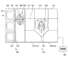
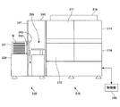
本実施の形態における基板処理システムについて説明する。
次に、本実施の形態におけるウエハWに対して処理を行う基板処理装置について説明する。本実施の形態における基板処理装置は、前述した基板処理システムにおける基板処理ユニット271〜274のいずれかに組み込まれているものである。
次に、本実施の形態における基板位置決め装置について説明する。
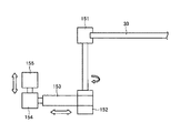
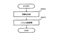
次に、図9に基づき、本実施の形態における基板位置決め方法について説明する。本実施の形態における基板の計測と位置決め方法は、図7及び図8に示す本実施の形態における基板位置決め装置を用いて行うものである。
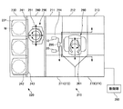
11 第1の基準部
12 支持部
13 第1の駆動部
14 接触面
15 ピン
16 ネジ
20 第2の位置決め機構部
21 第2の基準部
22 支持部
23 第2の駆動部
24 接触部
25 可動部
26 バネ部
27 本体部
28 位置センサ
29 連結部
30 基板
40 回転部
41 回転中心
44 真空チャック部
50 制御部
51 駆動制御部
52 記憶部
53 演算部
54 送信部
60 外部記憶部
Claims (15)
- 基板の位置決めを行うための基板位置決め装置において、
基板載置部と、
前記基板の側面と2点以上で接触させる第1の基準部を有する第1の位置決め機構部と、
前記第1の位置決め機構部を駆動させる第1の駆動部と、
接触部において前記基板の側面に接触する第2の基準部と、前記接触部に対し前記第1の駆動部の移動方向に力を加えることのできる弾性部と、前記第2の基準部の位置情報を検出するための検出部とを有する第2の位置決め機構部と、
前記第2の位置決め機構部を駆動させる第2の駆動部と、
前記第1の駆動部及び前記第2の駆動部を制御する制御部と、
を有し、
前記第1の基準部と前記第2の基準部は、前記基板載置部の中心が存在する同一線上に配置されており、
前記制御部は、前記第1の駆動部と第2の駆動部を制御して、前記第1の位置決め機構部及び前記第2の位置決め機構部を予め決められた基準位置まで移動させることにより、前記第1の基準部と前記基板の側面とを接触させ、さらに、前記第2の基準部と前記基板の側面とを接触させた後、前記検出部によって検出された位置情報に基づいて、前記基板の位置決めを行うことを特徴とする基板位置決め装置。 - 前記第2の基準部は、前記弾性部と前記検出部とが接続されている本体部と、前記弾性部と前記接触部とを接続する連結部とを有し、
前記接触部は、円形を有する形状であって、前記連結部に前記円形の中心を軸として回転可能な状態で取り付けられているものであって、前記基板とは一点で接触するものであることを特徴とする請求項1に記載の基板位置決め装置。 - 位置決めを行う際に基準とする基準基板に対する前記第1の位置決め機構部及び前記第2の位置決め機構部の基準位置情報を記憶する記憶部を有し、
前記制御部は、前記検出部によって検出された前記位置情報と前記基準位置情報との差を算出することにより前記基板の直径を算出し、前記基板の直径に基づき前記第1の位置決め機構部の位置を移動させて位置決めを行うことを特徴とする請求項1または2に記載の基板位置決め装置。 - 前記制御部は、前記基板の直径に基づいて補正値を算出し、前記補正値に基づき前記第1の位置決め機構部の位置を移動させて位置決めを行うことを特徴とする請求項3に記載の基板位置決め装置。
- 前記基板載置部は気体開口部を有し、前記気体開口部を介し前記基板に対し気体を供給または前記基板を吸引することを特徴とする請求項1から4のいずれかに記載の基板位置決め装置。
- 前記基板載置部を囲む下部カップと、前記下部カップの開口を覆うプレートとを有する前記基板を処理する基板処理部と、
請求項1から5のいずれかに記載の基板位置決め装置と、を備え
前記基板位置決め装置は、前記下部カップと前記プレートの間に進入して位置決めを行い、位置決め終了後は前記下部カップの外側に退避することを特徴とする基板処理装置。 - 基板の側面と2点以上で接触させる第1の基準部を有する第1の位置決め機構部と、接触部において前記基板の側面に接触する第2の基準部と、前記接触部に対し第1の駆動部の移動方向に力を加えることのできる弾性部と、前記第2の基準部の位置情報を検出するための検出部とを有する第2の位置決め機構部と、を用いて前記第1の基準部と前記第2の基準部を、基板載置部の中心が存在する同一線上に配置して行う、基板の位置決め方法において、
前記基板載置部上に基板を載置する基板載置工程と、
第1の位置決め機構部及び第2の位置決め機構部を予め決められた基準位置まで移動させる移動工程と、
前記基準位置において、前記基板の側面を第1の位置決め機構部における第1の基準部の接触面に接触させ、さらに、第2の位置決め機構部における第2の基準部の接触部に接触させた後、前記検出部により前記基板の位置を検出する検出工程と、
前記検出された位置情報に基づいて、前記基板の位置決めを行う基板位置決め工程と、
を有することを特徴とする基板位置決め方法。 - 前記基板位置決め工程では、前記検出した基板の位置情報に基づいて前記基板の直径を計測し、前記基板の直径に基づいて前記第1の位置決め機構部を前記基準位置より移動させることにより前記基板の位置決めを行うことを特徴とする請求項7に記載の基板位置決め方法。
- 前記検出工程において、前記第2の基準部の接触部が前記基板に接触する際、前記第2の基準部の接触部が接続されている弾性部が収縮することを特徴とする請求項7または8に記載の基板位置決め方法。
- 前記検出工程において、前記第2の基準部の接触部が、前記基板の動きに合わせて回転することを特徴とする請求項7から9のいずれかに記載の基板位置決め方法。
- 前記基板載置工程の前に、
基準となる大きさで形成された基準基板を前記基板載置部の中心と前記基準基板の中心とが一致するように、前記基板載置部上に載置する基準基板載置工程と、
前記第1の基準部の前記接触面と前記基準基板とを接触させ、前記第2の基準部の前記接触部と前記基準基板とを接触させることにより、前記第1の位置決め機構部と前記第2の位置決め機構部の前記基準位置を決定する基準位置決定工程と、
前記基準位置決定工程で決定された前記基準位置を記憶する記憶工程と、
を有することを特徴とする請求項7から10のいずれかに記載の基板位置決め方法。 - 前記基板位置決め工程は、
前記計測された前記基板の直径と、基準基板の直径との差を算出する比較工程と、
前記比較工程において得られた差に基づき、前記基板の中心と前記基板載置部の中心とが一致するように補正量を算出する補正量算出工程と、
前記補正量に基づき前記第1の位置決め機構部を移動させることにより、前記基板載置部上において、前記基板を前記補正量移動させる位置補正工程と、
を有することを特徴とする請求項8に記載の基板位置決め方法。 - 前記基板載置工程、前記基板位置決め工程においては、前記基板載置部より気体が供給されていることを特徴とする請求項7から12のいずれかに記載の基板位置決め方法。
- 前記基板位置決め工程の後に、前記基板載置部に前記基板が保持される基板保持工程を有することを特徴とする請求項7から13のいずれかに記載の基板位置決め方法。
- コンピュータに請求項7から14のいずれかに記載の基板位置決め方法を実行させるためのプログラムを記録したコンピュータ読取り可能な記録媒体。
Priority Applications (5)
| Application Number | Priority Date | Filing Date | Title |
|---|---|---|---|
| JP2011058278A JP5572575B2 (ja) | 2010-05-12 | 2011-03-16 | 基板位置決め装置、基板処理装置、基板位置決め方法及びプログラムを記録した記憶媒体 |
| KR1020110032787A KR101599086B1 (ko) | 2010-05-12 | 2011-04-08 | 기판 위치 결정 장치, 기판 처리 장치, 기판 위치 결정 방법, 및 프로그램을 기록한 기억 매체 |
| TW100115790A TWI509728B (zh) | 2010-05-12 | 2011-05-05 | 基板定位裝置、基板處理裝置、基板定位方法及記錄有程式之記憶媒體 |
| US13/104,374 US9008817B2 (en) | 2010-05-12 | 2011-05-10 | Substrate positioning apparatus, substrate processing apparatus, substrate positioning method, and computer readable medium having a program stored thereon |
| CN201110125137.6A CN102244026B (zh) | 2010-05-12 | 2011-05-12 | 基板定位装置、基板处理装置和基板定位方法 |
Applications Claiming Priority (3)
| Application Number | Priority Date | Filing Date | Title |
|---|---|---|---|
| JP2010110366 | 2010-05-12 | ||
| JP2010110366 | 2010-05-12 | ||
| JP2011058278A JP5572575B2 (ja) | 2010-05-12 | 2011-03-16 | 基板位置決め装置、基板処理装置、基板位置決め方法及びプログラムを記録した記憶媒体 |
Publications (3)
| Publication Number | Publication Date |
|---|---|
| JP2011258924A JP2011258924A (ja) | 2011-12-22 |
| JP2011258924A5 JP2011258924A5 (ja) | 2013-04-04 |
| JP5572575B2 true JP5572575B2 (ja) | 2014-08-13 |
Family
ID=44912452
Family Applications (1)
| Application Number | Title | Priority Date | Filing Date |
|---|---|---|---|
| JP2011058278A Active JP5572575B2 (ja) | 2010-05-12 | 2011-03-16 | 基板位置決め装置、基板処理装置、基板位置決め方法及びプログラムを記録した記憶媒体 |
Country Status (5)
| Country | Link |
|---|---|
| US (1) | US9008817B2 (ja) |
| JP (1) | JP5572575B2 (ja) |
| KR (1) | KR101599086B1 (ja) |
| CN (1) | CN102244026B (ja) |
| TW (1) | TWI509728B (ja) |
Cited By (1)
| Publication number | Priority date | Publication date | Assignee | Title |
|---|---|---|---|---|
| US10727090B2 (en) | 2017-05-31 | 2020-07-28 | SCREEN Holdings Co., Ltd. | Substrate processing apparatus and substrate processing method |
Families Citing this family (22)
| Publication number | Priority date | Publication date | Assignee | Title |
|---|---|---|---|---|
| JP5449239B2 (ja) * | 2010-05-12 | 2014-03-19 | 東京エレクトロン株式会社 | 基板処理装置、基板処理方法及びプログラムを記録した記憶媒体 |
| JP5243491B2 (ja) * | 2010-06-18 | 2013-07-24 | 東京エレクトロン株式会社 | 位置決め装置、基板処理装置及び基準部材の固定方法 |
| JP5727244B2 (ja) * | 2011-01-28 | 2015-06-03 | リンテック株式会社 | 支持装置及び支持方法 |
| JP5996381B2 (ja) * | 2011-12-28 | 2016-09-21 | 東京エレクトロン株式会社 | 基板処理装置および基板処理方法 |
| JP5835188B2 (ja) * | 2012-11-06 | 2015-12-24 | 東京エレクトロン株式会社 | 基板周縁部の塗布膜除去方法、基板処理装置及び記憶媒体 |
| CN103594406B (zh) * | 2013-11-05 | 2016-08-24 | 中国电子科技集团公司第四十五研究所 | 自定心定位卡盘及半导体晶圆的定心定位方法 |
| TWI668795B (zh) | 2014-09-15 | 2019-08-11 | 美商瓦里安半導體設備公司 | 半導體製程用的主動式基板對準系統及對準基板的方法 |
| JP6475756B2 (ja) * | 2015-02-04 | 2019-02-27 | 川崎重工業株式会社 | ロボットのぶれ自動調整装置及びロボットのぶれ自動調整方法 |
| JP6612670B2 (ja) * | 2016-03-31 | 2019-11-27 | 東京応化工業株式会社 | 基板処理装置、及び、基板処理方法 |
| CN108242417B (zh) * | 2016-12-26 | 2020-10-16 | 北京北方华创微电子装备有限公司 | 一种手动输送硅片机构 |
| JP6920849B2 (ja) * | 2017-03-27 | 2021-08-18 | 株式会社荏原製作所 | 基板処理方法および装置 |
| CN111217149B (zh) * | 2018-11-23 | 2024-08-27 | 合肥欣奕华智能机器股份有限公司 | 一种基板校准装置、基板校准方法及基板搬运装置 |
| CN114341398B (zh) | 2019-08-23 | 2024-10-29 | 朗姆研究公司 | 温控吊灯型喷头 |
| JP7426808B2 (ja) | 2019-11-27 | 2024-02-02 | 株式会社Screenホールディングス | 基板処理装置 |
| JP7637686B2 (ja) * | 2020-01-06 | 2025-02-28 | ラム リサーチ コーポレーション | 内部輪郭を有するフェースプレートを備えるシャワーヘッド |
| JP2022048506A (ja) * | 2020-09-15 | 2022-03-28 | 株式会社ダイヘン | アライナ装置 |
| CN113634401A (zh) * | 2021-09-08 | 2021-11-12 | 江苏科环新材料有限公司 | 一种纳米金属涂层加工装置 |
| CN114446848B (zh) * | 2021-12-28 | 2025-06-24 | 苏州精濑光电有限公司 | 一种料盒的辅助定位机构 |
| JP7813152B2 (ja) | 2022-02-07 | 2026-02-12 | 株式会社Screenホールディングス | センタリング装置、センタリング方法および基板処理装置 |
| KR102775356B1 (ko) * | 2022-12-21 | 2025-03-06 | 세메스 주식회사 | 편심 보정 유닛을 포함한 기판 처리 장치 및 기판 처리 방법 |
| KR102898065B1 (ko) * | 2023-10-17 | 2025-12-08 | 후쿠무라 코포레이션 | 열분해 탄화 처리 장치 |
| JP7801827B1 (ja) * | 2025-09-08 | 2026-01-19 | 株式会社オプトラン | アライメント装置及びアライメント方法 |
Family Cites Families (36)
| Publication number | Priority date | Publication date | Assignee | Title |
|---|---|---|---|---|
| JPH04274343A (ja) * | 1991-03-01 | 1992-09-30 | Fujitsu Ltd | 半導体ウエーハの位置決め装置と位置決め方法 |
| TW319751B (ja) * | 1995-05-18 | 1997-11-11 | Toshiba Co Ltd | |
| JPH1089904A (ja) * | 1996-09-17 | 1998-04-10 | Hitachi Electron Eng Co Ltd | Vノッチウェハ位置決め装置 |
| JP4547524B2 (ja) * | 2000-12-05 | 2010-09-22 | 川崎重工業株式会社 | ワーク処理方法、ワーク処理装置およびロボット |
| JP4389424B2 (ja) * | 2001-12-25 | 2009-12-24 | 東京エレクトロン株式会社 | 被処理体の搬送機構及び処理システム |
| JP4173309B2 (ja) * | 2002-01-28 | 2008-10-29 | 東京エレクトロン株式会社 | センタリング装置及び枚葉式検査装置 |
| US20030168175A1 (en) * | 2002-03-08 | 2003-09-11 | Kim Kyung-Tae | Substrate alignment apparatus |
| JP3956350B2 (ja) * | 2002-03-25 | 2007-08-08 | 東京エレクトロン株式会社 | 位置決め機能を有する基板処理装置及び位置決め機能を有する基板処理方法 |
| US6700090B2 (en) * | 2002-04-26 | 2004-03-02 | Hitachi High-Technologies Corporation | Plasma processing method and plasma processing apparatus |
| US7367773B2 (en) * | 2002-05-09 | 2008-05-06 | Maxtor Corporation | Apparatus for combining or separating disk pairs simultaneously |
| US7499767B2 (en) * | 2003-02-20 | 2009-03-03 | Applied Materials, Inc. | Methods and apparatus for positioning a substrate relative to a support stage |
| JP2004342939A (ja) | 2003-05-16 | 2004-12-02 | Shimada Phys & Chem Ind Co Ltd | 基板処理装置 |
| JP4304692B2 (ja) * | 2003-06-27 | 2009-07-29 | ローツェ株式会社 | 円盤状物の把持を確認するクランプ装置 |
| WO2005055312A1 (ja) * | 2003-12-04 | 2005-06-16 | Hirata Corporation | 基板位置決めシステム |
| KR101003666B1 (ko) * | 2003-12-10 | 2010-12-23 | 엘지디스플레이 주식회사 | 정렬장치 |
| US7824498B2 (en) * | 2004-02-24 | 2010-11-02 | Applied Materials, Inc. | Coating for reducing contamination of substrates during processing |
| JP2005262367A (ja) * | 2004-03-18 | 2005-09-29 | Tokyo Electron Ltd | 搬送ロボットの搬送ズレ確認方法及び処理装置 |
| JP4502199B2 (ja) * | 2004-10-21 | 2010-07-14 | ルネサスエレクトロニクス株式会社 | エッチング装置およびエッチング方法 |
| US7547181B2 (en) * | 2004-11-15 | 2009-06-16 | Dainippon Screen Mfg. Co., Ltd. | Substrate position correcting method and apparatus using either substrate radius or center of rotation correction adjustment sum |
| US20090017733A1 (en) * | 2005-04-19 | 2009-01-15 | Ebara Corporation | Substrate processing apparatus |
| JP4892225B2 (ja) * | 2005-10-28 | 2012-03-07 | 株式会社日立ハイテクノロジーズ | 真空処理方法、真空搬送装置および半導体処理装置 |
| JP4657090B2 (ja) | 2005-11-17 | 2011-03-23 | 大日本スクリーン製造株式会社 | 基板処理装置 |
| JP4781802B2 (ja) * | 2005-12-06 | 2011-09-28 | 東京応化工業株式会社 | サポートプレートの貼り合わせ手段及び貼り合わせ装置、並びにサポートプレートの貼り合わせ方法 |
| JP4698407B2 (ja) * | 2005-12-20 | 2011-06-08 | 大日本スクリーン製造株式会社 | 基板処理装置および基板処理方法 |
| JP4961895B2 (ja) * | 2006-08-25 | 2012-06-27 | 東京エレクトロン株式会社 | ウェハ搬送装置、ウェハ搬送方法及び記憶媒体 |
| JP5030542B2 (ja) * | 2006-11-10 | 2012-09-19 | 株式会社日立ハイテクノロジーズ | 真空処理装置 |
| JP2008173744A (ja) * | 2007-01-22 | 2008-07-31 | Tokyo Electron Ltd | 搬送システムの搬送位置合わせ方法 |
| US20090110532A1 (en) * | 2007-10-29 | 2009-04-30 | Sokudo Co., Ltd. | Method and apparatus for providing wafer centering on a track lithography tool |
| JP2009130011A (ja) | 2007-11-21 | 2009-06-11 | Atel Corp | 基板位置決め装置 |
| JP5435861B2 (ja) * | 2007-12-13 | 2014-03-05 | 芝浦メカトロニクス株式会社 | 電子部品の実装装置及び実装方法 |
| JP4926933B2 (ja) * | 2007-12-14 | 2012-05-09 | 東京エレクトロン株式会社 | 基板洗浄装置および基板洗浄方法 |
| US7963736B2 (en) * | 2008-04-03 | 2011-06-21 | Asm Japan K.K. | Wafer processing apparatus with wafer alignment device |
| JP5301505B2 (ja) * | 2009-08-27 | 2013-09-25 | 東京エレクトロン株式会社 | 液処理装置および液処理方法 |
| JP5449239B2 (ja) * | 2010-05-12 | 2014-03-19 | 東京エレクトロン株式会社 | 基板処理装置、基板処理方法及びプログラムを記録した記憶媒体 |
| JP5243491B2 (ja) * | 2010-06-18 | 2013-07-24 | 東京エレクトロン株式会社 | 位置決め装置、基板処理装置及び基準部材の固定方法 |
| JP5729326B2 (ja) * | 2012-02-14 | 2015-06-03 | 東京エレクトロン株式会社 | 液処理装置、液処理方法及び記憶媒体 |
-
2011
- 2011-03-16 JP JP2011058278A patent/JP5572575B2/ja active Active
- 2011-04-08 KR KR1020110032787A patent/KR101599086B1/ko active Active
- 2011-05-05 TW TW100115790A patent/TWI509728B/zh active
- 2011-05-10 US US13/104,374 patent/US9008817B2/en active Active
- 2011-05-12 CN CN201110125137.6A patent/CN102244026B/zh active Active
Cited By (1)
| Publication number | Priority date | Publication date | Assignee | Title |
|---|---|---|---|---|
| US10727090B2 (en) | 2017-05-31 | 2020-07-28 | SCREEN Holdings Co., Ltd. | Substrate processing apparatus and substrate processing method |
Also Published As
| Publication number | Publication date |
|---|---|
| JP2011258924A (ja) | 2011-12-22 |
| CN102244026A (zh) | 2011-11-16 |
| US20110282484A1 (en) | 2011-11-17 |
| TW201205712A (en) | 2012-02-01 |
| KR20110125166A (ko) | 2011-11-18 |
| CN102244026B (zh) | 2016-04-20 |
| KR101599086B1 (ko) | 2016-03-14 |
| US9008817B2 (en) | 2015-04-14 |
| TWI509728B (zh) | 2015-11-21 |
Similar Documents
| Publication | Publication Date | Title |
|---|---|---|
| JP5572575B2 (ja) | 基板位置決め装置、基板処理装置、基板位置決め方法及びプログラムを記録した記憶媒体 | |
| JP5449239B2 (ja) | 基板処理装置、基板処理方法及びプログラムを記録した記憶媒体 | |
| US9799540B2 (en) | Liquid processing apparatus, liquid processing method and storage medium | |
| JP6363605B2 (ja) | フィルムフレーム上のウェハーの回転ミスアライメントを自動的に訂正するためのシステム及び方法 | |
| CN110050336B (zh) | 用于制造半导体装置的晶片边缘提升销设计 | |
| KR101423811B1 (ko) | 위치 결정 장치, 기판 처리 장치 및 기준 부재의 고정 방법 | |
| US20150044008A1 (en) | Robot Blade Design | |
| US20090092470A1 (en) | End effector with sensing capabilities | |
| TWI839869B (zh) | 基板處理裝置及基板處理方法 | |
| CN216980525U (zh) | 一种晶圆对准装置 | |
| JP6756600B2 (ja) | 基板処理装置および基板処理方法 | |
| JP7791053B2 (ja) | ノズル位置調整方法および基板処理装置 | |
| US20250014917A1 (en) | Separating apparatus, separating system and separating method | |
| US20250012606A1 (en) | Distance measuring device, distance measuring method, bonding apparatus, and bonding method | |
| US20250014916A1 (en) | Separating apparatus, separating system and separating method | |
| JP2025042743A (ja) | センタリング装置、センタリング方法および基板処理装置 | |
| KR100686453B1 (ko) | 반도체 웨이퍼 파드 | |
| JP2024164427A (ja) | 接合装置、接合システムおよび接合方法 | |
| JP2024106617A (ja) | センタリング装置、センタリング方法および基板処理装置 | |
| KR20050037828A (ko) | 웨이퍼 이송로봇의 칼리브레이션 장치 |
Legal Events
| Date | Code | Title | Description |
|---|---|---|---|
| A521 | Request for written amendment filed |
Free format text: JAPANESE INTERMEDIATE CODE: A523 Effective date: 20130218 |
|
| A621 | Written request for application examination |
Free format text: JAPANESE INTERMEDIATE CODE: A621 Effective date: 20130218 |
|
| A977 | Report on retrieval |
Free format text: JAPANESE INTERMEDIATE CODE: A971007 Effective date: 20131216 |
|
| A131 | Notification of reasons for refusal |
Free format text: JAPANESE INTERMEDIATE CODE: A131 Effective date: 20140107 |
|
| A521 | Request for written amendment filed |
Free format text: JAPANESE INTERMEDIATE CODE: A523 Effective date: 20140303 |
|
| TRDD | Decision of grant or rejection written | ||
| A01 | Written decision to grant a patent or to grant a registration (utility model) |
Free format text: JAPANESE INTERMEDIATE CODE: A01 Effective date: 20140603 |
|
| A61 | First payment of annual fees (during grant procedure) |
Free format text: JAPANESE INTERMEDIATE CODE: A61 Effective date: 20140630 |
|
| R150 | Certificate of patent or registration of utility model |
Ref document number: 5572575 Country of ref document: JP Free format text: JAPANESE INTERMEDIATE CODE: R150 |
|
| R250 | Receipt of annual fees |
Free format text: JAPANESE INTERMEDIATE CODE: R250 |
|
| R250 | Receipt of annual fees |
Free format text: JAPANESE INTERMEDIATE CODE: R250 |
|
| R250 | Receipt of annual fees |
Free format text: JAPANESE INTERMEDIATE CODE: R250 |
|
| R250 | Receipt of annual fees |
Free format text: JAPANESE INTERMEDIATE CODE: R250 |
|
| R250 | Receipt of annual fees |
Free format text: JAPANESE INTERMEDIATE CODE: R250 |
|
| R250 | Receipt of annual fees |
Free format text: JAPANESE INTERMEDIATE CODE: R250 |
|
| R250 | Receipt of annual fees |
Free format text: JAPANESE INTERMEDIATE CODE: R250 |