JP5572575B2 - Substrate positioning apparatus, substrate processing apparatus, substrate positioning method, and storage medium storing program - Google Patents
Substrate positioning apparatus, substrate processing apparatus, substrate positioning method, and storage medium storing program Download PDFInfo
- Publication number
- JP5572575B2 JP5572575B2 JP2011058278A JP2011058278A JP5572575B2 JP 5572575 B2 JP5572575 B2 JP 5572575B2 JP 2011058278 A JP2011058278 A JP 2011058278A JP 2011058278 A JP2011058278 A JP 2011058278A JP 5572575 B2 JP5572575 B2 JP 5572575B2
- Authority
- JP
- Japan
- Prior art keywords
- substrate
- positioning
- unit
- contact
- positioning mechanism
- Prior art date
- Legal status (The legal status is an assumption and is not a legal conclusion. Google has not performed a legal analysis and makes no representation as to the accuracy of the status listed.)
- Active
Links
Images


Classifications
-
- H—ELECTRICITY
- H10—SEMICONDUCTOR DEVICES; ELECTRIC SOLID-STATE DEVICES NOT OTHERWISE PROVIDED FOR
- H10P—GENERIC PROCESSES OR APPARATUS FOR THE MANUFACTURE OR TREATMENT OF DEVICES COVERED BY CLASS H10
- H10P72/00—Handling or holding of wafers, substrates or devices during manufacture or treatment thereof
- H10P72/50—Handling or holding of wafers, substrates or devices during manufacture or treatment thereof for positioning, orientation or alignment
-
- H—ELECTRICITY
- H10—SEMICONDUCTOR DEVICES; ELECTRIC SOLID-STATE DEVICES NOT OTHERWISE PROVIDED FOR
- H10P—GENERIC PROCESSES OR APPARATUS FOR THE MANUFACTURE OR TREATMENT OF DEVICES COVERED BY CLASS H10
- H10P72/00—Handling or holding of wafers, substrates or devices during manufacture or treatment thereof
- H10P72/04—Apparatus for manufacture or treatment
- H10P72/0402—Apparatus for fluid treatment
- H10P72/0406—Apparatus for fluid treatment for cleaning followed by drying, rinsing, stripping, blasting or the like
- H10P72/0411—Apparatus for fluid treatment for cleaning followed by drying, rinsing, stripping, blasting or the like for wet cleaning or washing
- H10P72/0412—Apparatus for fluid treatment for cleaning followed by drying, rinsing, stripping, blasting or the like for wet cleaning or washing using mainly scrubbing means, e.g. brushes
-
- H—ELECTRICITY
- H10—SEMICONDUCTOR DEVICES; ELECTRIC SOLID-STATE DEVICES NOT OTHERWISE PROVIDED FOR
- H10P—GENERIC PROCESSES OR APPARATUS FOR THE MANUFACTURE OR TREATMENT OF DEVICES COVERED BY CLASS H10
- H10P72/00—Handling or holding of wafers, substrates or devices during manufacture or treatment thereof
- H10P72/04—Apparatus for manufacture or treatment
- H10P72/0402—Apparatus for fluid treatment
- H10P72/0406—Apparatus for fluid treatment for cleaning followed by drying, rinsing, stripping, blasting or the like
- H10P72/0411—Apparatus for fluid treatment for cleaning followed by drying, rinsing, stripping, blasting or the like for wet cleaning or washing
- H10P72/0414—Apparatus for fluid treatment for cleaning followed by drying, rinsing, stripping, blasting or the like for wet cleaning or washing using mainly spraying means, e.g. nozzles
Landscapes
- Container, Conveyance, Adherence, Positioning, Of Wafer (AREA)
Description
本発明は、基板位置決め装置、基板処理装置、基板位置決め方法及びプログラムを記録した記憶媒体に関する。 The present invention relates to a substrate positioning apparatus, a substrate processing apparatus, a substrate positioning method, and a storage medium on which a program is recorded.
半導体メモリ等の半導体素子は、半導体ウエハ等の基板上において成膜、エッチング等の基板処理を行うことにより形成される。このような基板処理として、基板の周辺部を処理するベベル処理等があり、このようなベベル処理等はベベル処理を行う基板処理装置により行われる。 A semiconductor element such as a semiconductor memory is formed by performing substrate processing such as film formation and etching on a substrate such as a semiconductor wafer. Such substrate processing includes bevel processing for processing the peripheral portion of the substrate, and such bevel processing is performed by a substrate processing apparatus that performs bevel processing.
ところで、ベベル処理は、半導体ウエハ等の基板を回転させながら処理を行うものであるため、半導体ウエハ等の基板の中心と回転中心とが一致している必要があり、ベベル処理される半導体ウエハ等の基板の位置決めが極めて重要である。これは、ベベル処理が基板の側面(端部)から数ミリの領域において行われるため、基板処理装置において基板が所定の位置よりずれて設置されてしまうと、所望のベベル処理が行われず、製造される半導体素子の歩留まりの低下等を招いてしまうからである。 By the way, since the bevel process is performed while rotating a substrate such as a semiconductor wafer, the center of the substrate such as a semiconductor wafer needs to coincide with the rotation center. The positioning of the substrate is very important. This is because the bevel processing is performed in a region of several millimeters from the side surface (end portion) of the substrate, so that if the substrate is placed out of a predetermined position in the substrate processing apparatus, the desired bevel processing is not performed and the manufacturing is performed. This is because the yield of the semiconductor device to be reduced is reduced.
また、ベベル処理を行う基板処理装置以外にも、半導体ウエハ等の基板を回転させながら処理を行う基板処理装置として、半導体ウエハ等の基板の中心から周辺に向けて処理を行う基板処理装置、また、基板の周辺から中心に向けて処理を行う基板処理装置等があり、これらの基板処理装置においても、回転中心に対する基板中心の正確な位置決めが要求される。 In addition to a substrate processing apparatus that performs bevel processing, as a substrate processing apparatus that performs processing while rotating a substrate such as a semiconductor wafer, a substrate processing apparatus that performs processing from the center of the substrate such as a semiconductor wafer toward the periphery, or There are substrate processing apparatuses that perform processing from the periphery of the substrate toward the center, and these substrate processing apparatuses also require accurate positioning of the substrate center with respect to the rotation center.
このような半導体ウエハ等の基板の位置決めを行う方法としては、引用文献1及び2に開示されている。 References 1 and 2 disclose a method for positioning a substrate such as a semiconductor wafer.
しかしながら、300mmウエハ等の大型な基板の場合等では、回転中心に対し基板の中心を正確に位置決めすることは極めて困難であり、特許文献1及び2に記載されている方法では、十分に対応することができない。また、半導体ウエハは、製造誤差や製造の都合上、全く同一の直径の半導体ウエハを製造することは困難であり、同じ300mmウエハでも、所定の規格を満たす範囲内で、大きさが異なるものが供給されているのが現状である。 However, in the case of a large substrate such as a 300 mm wafer, it is extremely difficult to accurately position the center of the substrate with respect to the rotation center, and the methods described in Patent Documents 1 and 2 are sufficient. I can't. In addition, it is difficult to manufacture a semiconductor wafer having exactly the same diameter due to manufacturing errors and manufacturing reasons. Even with the same 300 mm wafer, the size of the semiconductor wafer is different within a range that satisfies a predetermined standard. It is currently being supplied.
このため、大きさが異なる半導体ウエハ等の基板においても、半導体ウエハ等の基板の中心と回転中心とが一致するように位置決めを行うことができる基板位置決め装置、基板位置決め方法が望まれており、更には、このような基板位置決め装置を有する基板処理装置及びプログラムを記録した記憶媒体が望まれている。 For this reason, a substrate positioning apparatus and a substrate positioning method that can perform positioning so that the center of a substrate such as a semiconductor wafer and the center of rotation coincide with each other even in substrates having different sizes are desired. Furthermore, a substrate processing apparatus having such a substrate positioning apparatus and a storage medium storing a program are desired.
本発明は、基板の位置決めを行うための基板位置決め装置において、基板載置部と、前記基板の側面と2点以上で接触させる第1の基準部を有する第1の位置決め機構部と、前記第1の位置決め機構部を駆動させる第1の駆動部と、接触部において前記基板の側面に接触する第2の基準部と、前記接触部に対し前記第1の駆動部の移動方向に力を加えることのできる弾性部と、前記第2の基準部の位置情報を検出するための検出部とを有する第2の位置決め機構部と、前記第2の位置決め機構部を駆動させる第2の駆動部と、前記第1の駆動部及び前記第2の駆動部を制御する制御部と、を有し、前記第1の基準部と前記第2の基準部は、前記基板載置部の中心が存在する同一線上に配置されており、前記制御部は、前記第1の駆動部と第2の駆動部を制御して、前記第1の位置決め機構部及び前記第2の位置決め機構部を予め決められた基準位置まで移動させることにより、前記第1の基準部と前記基板の側面とを接触させ、さらに、前記第2の基準部と前記基板の側面とを接触させた後、前記検出部によって検出された位置情報に基づいて、前記基板の位置決めを行うことを特徴とする。
The present invention provides a substrate positioning apparatus for positioning the substrate, and a first positioning mechanism having a board mounting portion, the side surface and the first reference portion of Ru is contacted with two or more points of the substrate, wherein A first driving unit that drives the first positioning mechanism unit, a second reference unit that contacts the side surface of the substrate at the contact unit, and a force in the moving direction of the first driving unit with respect to the contact unit A second positioning mechanism section having an elastic section that can be added, and a detection section for detecting position information of the second reference section; and a second driving section that drives the second positioning mechanism section And a control unit that controls the first driving unit and the second driving unit, and the first reference unit and the second reference unit have a center of the substrate mounting unit. Are arranged on the same line, and the control unit includes the first driving unit and the second driving unit. By controlling the drive unit to move the first positioning mechanism unit and the second positioning mechanism unit to a predetermined reference position, the first reference unit and the side surface of the substrate are brought into contact with each other. Further, the substrate is positioned based on the position information detected by the detection unit after the second reference unit and the side surface of the substrate are brought into contact with each other.
また、本発明は、基板の側面と2点以上で接触させる第1の基準部を有する第1の位置決め機構部と、接触部において前記基板の側面に接触する第2の基準部と、前記接触部に対し第1の駆動部の移動方向に力を加えることのできる弾性部と、前記第2の基準部の位置情報を検出するための検出部とを有する第2の位置決め機構部と、を用いて前記第1の基準部と前記第2の基準部を、基板載置部の中心が存在する同一線上に配置して行う、基板の位置決め方法において、前記基板載置部上に基板を載置する基板載置工程と、第1の位置決め機構部及び第2の位置決め機構部を予め決められた基準位置まで移動させる移動工程と、前記基準位置において、前記基板の側面を第1の位置決め機構部における第1の基準部の接触面に接触させ、さらに、第2の位置決め機構部における第2の基準部の接触部に接触させた後、前記検出部により前記基板の位置を検出する検出工程と、前記検出された位置情報に基づいて、前記基板の位置決めを行う基板位置決め工程と、を有することを特徴とする。
In addition, the present invention provides a first positioning mechanism having a first reference portion that contacts the side surface of the substrate at two or more points, a second reference portion that contacts the side surface of the substrate at the contact portion, and the contact A second positioning mechanism section having an elastic section capable of applying a force to the section in the moving direction of the first drive section and a detection section for detecting position information of the second reference section. the second reference portion and the first reference portion used performs arranged on the same line where the center of the substrate placement portion is present, in the positioning method of a substrate, placing the substrate on the substrate mounting portion A substrate placing step for placing, a moving step for moving the first positioning mechanism portion and the second positioning mechanism portion to a predetermined reference position, and a side surface of the substrate at the reference position at the first positioning mechanism. In contact with the contact surface of the first reference part To, after the contact with the contact portion of the second reference portion of the second positioning mechanism, a detection step for detecting a position of the substrate by the detection unit, based on the detected position information, said substrate And a substrate positioning step for performing positioning.
本発明によれば、大きさが異なる半導体ウエハ等の基板においても、基板の位置決めを正確に行うことができる基板位置決め装置、基板位置決め方法、更には、このような基板位置決め装置を有する基板処理装置及びプログラムを記録した記憶媒体を提供することができる。 According to the present invention, a substrate positioning apparatus, a substrate positioning method, and a substrate processing apparatus having such a substrate positioning apparatus can accurately position a substrate even on substrates such as semiconductor wafers of different sizes. And a storage medium recording the program.
本発明を実施するための形態について、以下に説明する。 The form for implementing this invention is demonstrated below.
(基板処理システム)
本実施の形態における基板処理システムについて説明する。
(Substrate processing system)
A substrate processing system in this embodiment will be described.
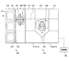
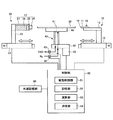
図1及び図2に基づき、本実施の形態における基板処理システムについて説明する。尚、図1は、この基板処理システムの横断面図であり、図2は、側面図である。この基板処理ユニットは、基板処理を行う基板処理部210と、外部と基板処理部210との間でウエハWの搬入出を行う搬入出部220とを有している。
The substrate processing system in the present embodiment will be described based on FIGS. 1 is a cross-sectional view of the substrate processing system, and FIG. 2 is a side view. The substrate processing unit includes a
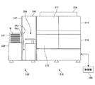
搬入出部220には、複数枚、例えば、25枚のウエハを収容することのできるFOUP(Front Opening Unified Pod)231を載置するための載置台230と、載置台230に載置されたFOUP231と基板処理部210との間でウエハWの受け渡しを行うための搬送室240とが設けられている。FOUP231には、複数枚のウエハWが、略水平状態で保持されており、鉛直方向に所定の間隔となるように収納されている。
In the loading /
載置台230は、搬送室240の側壁部241に沿って配置されており、例えば、3個のFOUP231が所定の位置に載置されている。側壁部241には、FOUP231の載置場所に対応する位置に、開口部242が設けられており、更に、各々の開口部242に設けられたシャッタ243が開閉することにより、FOUP231との間でウエハWの搬入出を行うことができるように構成されている。搬送室240内には、FOUP231と基板処理部210との間でウエハWを搬送する第1のウエハ搬送機構250が設けられている。第1のウエハ搬送機構250は、進退、昇降、回転の全てが自在に構成されたピック251を備えており、このピック251上にウエハWが保持されて搬送される。また、ピック251は、基板処理部210に設けられているウエハ受け渡しユニット214に進入することが可能であり、ウエハ受け渡しユニット214にピック251を進入させることにより、基板処理部210との間においてウエハWの受け渡しを行うことができる。
The mounting table 230 is disposed along the
基板処理部210は、搬送室240との間で受け渡しされるウエハWを一時的に載置するウエハ受け渡しユニット214と、ウエハWにおける基板処理を行う基板処理ユニット271〜274と、基板処理部210においてウエハWの搬送を行う第2のウエハ搬送機構260が設けられている。また、基板処理ユニット271〜274のいずれかには、後述する本実施の形態におけるベベル処理装置等の基板処理装置と基板位置決め装置とが組み込まれている。また、第2のウエハ搬送機構260は、進退、昇降、回転の全てが自在に構成されたピック261を備えており、このピック261上にウエハWが保持されて搬送される。更に、基板処理部210には、ベベル処理等を行うための処理液を貯蔵するための処理液貯蔵ユニット211と、基板処理システム全体に電力を供給するための電源ユニット212と、基板処理システム全体の制御を行う機械制御部213が設けられている。また、基板処理部210の天井部分には、各々のユニット及び第2のウエハ搬送機構260が設けられている空間に清浄な空気をダウンフローにより供給するためのファンフィルタユニット(FFU)216が設けられている。
The
また、この基板処理システムは、制御部280が接続されている。この制御部280は、例えば、不図示のCPUと記憶部とを備えたコンピュータにより構成されており、記憶部には、基板処理システムにおいて行われる動作を制御するためのプログラムが記憶されている。このプログラムは、例えば、ハードディスク、コンパクトディスク、マグネットオプティカルディスク、メモリカード等の記憶媒体に格納され、そこからコンピュータにインストールされる。また、この制御部280は、例えば、基板処理部210における機械制御ユニット213内に設けてもよい。
In addition, the substrate processing system is connected to a
尚、本実施の形態における基板処理システムは複数の処理ユニットを有するものであるが、基板処理装置としての概念に含まれるものである。 The substrate processing system in the present embodiment has a plurality of processing units, but is included in the concept as a substrate processing apparatus.
(基板処理装置)
次に、本実施の形態におけるウエハWに対して処理を行う基板処理装置について説明する。本実施の形態における基板処理装置は、前述した基板処理システムにおける基板処理ユニット271〜274のいずれかに組み込まれているものである。
(Substrate processing equipment)
Next, a substrate processing apparatus for processing the wafer W in the present embodiment will be described. The substrate processing apparatus in the present embodiment is incorporated in any of the
本実施の形態における基板処理装置は、例えば、ウエハWのベベル処理を行うベベル処理装置である。具体的には、本実施の形態におけるベベル処理装置は、ウエハWを回転させながら、ウエハWの側面(端部)から内側に3mm程度までの領域の処理を行う装置であり、この部分に形成されているSiO2膜、SiN膜、ポリシリコン膜等をフッ酸(HF)、アンモニア(NH3)と過酸化水素(H2O2)との混合溶液、フッ硝酸(フッ酸と硝酸(HNO3)の混合液)等の処理液により、除去するための基板処理装置である。尚、本願明細書において上述したウエハWは後述する基板30に相当するものであり、半導体ウエハと称するものである。
The substrate processing apparatus in the present embodiment is, for example, a bevel processing apparatus that performs bevel processing of the wafer W. Specifically, the bevel processing apparatus in the present embodiment is an apparatus that processes a region from the side surface (end) of the wafer W to about 3 mm while rotating the wafer W, and is formed in this portion. The SiO 2 film, the SiN film, the polysilicon film, etc. that have been formed are mixed with hydrofluoric acid (HF), ammonia (NH 3 ) and hydrogen peroxide (H 2 O 2 ), hydrofluoric acid (hydrofluoric acid and nitric acid (HNO). 3 ) A substrate processing apparatus for removing with a processing liquid such as a mixed liquid). Incidentally, the wafer W described above in this specification corresponds to a
図3及び図4に基づき、本実施の形態における基板処理装置としてベベル処理装置について説明する。本実施の形態におけるベベル処理装置は、ベベル処理に用いられた処理液を受け、ベベル処理装置の外部に排出するためのドレインカップ110、基板30の上方を覆うためのトッププレート120、基板30を載置し回転させるための回転部40、ノズル部140及び160、図5に示すブラシユニット150を有しており、更に、後述する基板位置決め装置を有している。図3は、ドレインカップ110とトッププレート120とが開いて基板の搬出入が可能な状態を示し、図4は、ドレインカップ110とトッププレート120とが閉じた状態を示す。尚、ベベル処理は、図4に示すようにドレインカップ110とトッププレート120とが閉じた状態で行われる。
Based on FIGS. 3 and 4, a bevel processing apparatus will be described as a substrate processing apparatus in the present embodiment. The bevel processing apparatus in the present embodiment includes a
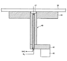
図6に示すように、回転部40は、回転伝達部42を介してモータ43が設けられており、基板30を載置して回転させることができる。また、回転部40において基板30が設置される面には、基板吸着部となる真空チャック部44が設けられており、不図示の真空ポンプ等に接続されている。真空チャック部44には気体開口部47が設けられており、真空チャック部44における真空チャックは、基板30を真空チャック部44に載置した後、真空ポンプ等により排気することにより、気体開口部47に基板30が吸着されることにより行われる。また、真空チャック部44においては、気体開口部47より窒素(N2)ガス等を基板30側に供給すること(窒素ガスブロー)により、真空チャック部44上において基板30を浮上させることも可能である。
As shown in FIG. 6, the
本実施の形態では、回転部40における真空チャック部44上に基板30を載置した後、後述するドレインカップ110の外側に備えられた基板位置決め装置がドレインカップ110とトッププレート120の間に進入することにより、基板30の中心位置の位置決めを行う。その後、基板位置決め装置をドレインカップ110とトッププレート120の間に進入した位置からドレインカップ110の外側に退避させてから、トッププレート120を降下させ、かつ、ドレインカップ110を上昇させて、トッププレート120とドレインカップ110とが接触した状態で、処理空間を形成する。その処理空間内において、基板30を回転させて、トッププレート120側に設けられたノズル部140における第1のノズル141と、ドレインカップ110側に設けられたノズル部160における第2のノズル161より処理液を供給し、基板30のべベル処理を行う。
In the present embodiment, after placing the
また、ノズル部140には第1のノズル141を基板30の半径方向に移動させるためのモータ142が設けられており、ノズル部160には第2のノズル161をウエハの半径方向に移動させるためのモータ162が設けられている。これらの第1のノズル141及び第2のノズル161は、後述する基板位置決め装置により得られた基板の直径等の情報に基づいて決定された位置に、モータ142及びモータ162により、配置される。この際、ノズル駆動部となるモータ142及びモータ162は、ノズル駆動制御部170の制御により、第1のノズル141及び第2のノズル161を移動させる。これにより基板の大きさに依存することなく所望のベベル処理を確実に行うことができる。
The
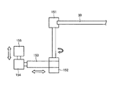
また、本実施の形態における基板処理装置では、図5に示すように、ブラシユニット150を有しており、ブラシユニット150による処理を行うことができる。このブラシユニット150は、基板30に接触して処理を行う円柱形にスポンジ等により形成されたブラシ部151、ブラシ部151を回転させるためのブラシ用モータ152を有し、ブラシ部151及びブラシ用モータ152を含むブラシユニット本体部153を移動させることのできる第1のモータ154及び第2のモータ155を有している。そして、このブラシユニット150は、ドレインカップ110とトッププレート120とが閉じた状態で、基板30の処理を行う。第1のモータ154は、基板面に対し平行方向にブラシユニット本体部153を移動させることができるものであり、ブラシ部151の基板30に対する水平方向の位置を調整することができる。よって、第1のモータ154により、基板30の処理がなされる領域を定めることができる。また、第2のモータ155は、基板面に対し垂直方向にブラシユニット本体部153を移動させることができるものであり、ブラシ部151の基板30に対する高さを調整することができる。よって、第2のモータ155により、ブラシ部151が、所望の押圧力で基板30の処理を行うことができる所定の高さに調整することができる。本実施の形態では、後述する基板位置決め装置により得られた基板30の直径等の情報に基づいて、第1のモータ154を制御し、基板30の大きさに対応して、ブラシ部151を所望の位置に移動させることができる。これにより、ブラシ部151による基板30の処理を最適な位置で行うことができ、所望の処理を行うことができる。
Further, the substrate processing apparatus in the present embodiment has a brush unit 150 as shown in FIG. 5, and can perform processing by the brush unit 150. The brush unit 150 has a
(基板位置決め装置)
次に、本実施の形態における基板位置決め装置について説明する。
(Substrate positioning device)
Next, the substrate positioning apparatus in the present embodiment will be described.
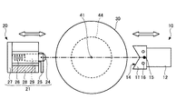
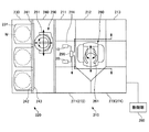
図7は、本実施の形態における基板位置決め装置の側面図であり、図8は、本実施の形態における基板位置決め装置の上面図である。本実施の形態における基板位置決め装置は、半導体ウエハ等の円形の基板の位置決めを行うものである。 FIG. 7 is a side view of the substrate positioning apparatus in the present embodiment, and FIG. 8 is a top view of the substrate positioning apparatus in the present embodiment. The substrate positioning apparatus in the present embodiment is for positioning a circular substrate such as a semiconductor wafer.
本実施の形態における基板位置決め装置は、基板処理ユニット271〜274のいずれかに組み込まれており、第1の位置決め機構部10と第2の位置決め機構部20とを有している。第1の位置決め機構部10と第2の位置決め機構部20とは、基板30を設置する回転部40の回転中心41を通る直線上に回転部40を挟んで対向する位置に配置されている。
The substrate positioning apparatus in the present embodiment is incorporated in one of the
第1の位置決め機構部10は、基板30の側面(端部)と接触する第1の基準部11、第1の基準部11を支持するための支持部12及び支持部12を介し第1の基準部11を基板30の半径方向に直線的に移動させることのできる第1の駆動部13を有している。第1の基準部11は、基板30と接触する接触面14が上面から見てV字状に形成されており、この接触面14において円形の基板30の側面の2点と接触することができるように形成されている。第1の基準部11は、変形しない材料であって、金属等の不純物が混入する可能性の少ない材料が好ましく、例えば、セラミックスまたはポリエーテル・エーテル・ケトン樹脂(PEEK)等の樹脂材料により形成されている。支持部12は、L字に形成されており、一方の端において、第1の基準部11が取り付けられている。第1の基準部11は、支持部12に設けられたピン15を中心に回転可能な状態で支持されるとともに、ネジ16により固定されている。
The first
この際、ピン15を中心に第1の基準部11を動かし、後述する基準基板81の側面の2点と接触する位置に合わせ、ネジ16により固定することにより、第1の基準部11と基準基板81とを確実に2点で接触させることができる。また、支持部12の他方の端は、第1の駆動部13に接続されている。第1の駆動部13は、第1の基準部11を基板30の半径方向に直線的に移動させることができるものであって、所定の位置で停止させることができる位置制御可能なモータにより構成されている。例えば、位置制御を比較的正確に行うことが可能なステッピングモータ等が好ましい。
At this time, the
第2の位置決め機構部20は、基板30の側面と接触する第2の基準部21、第2の基準部21を支持するための支持部22及び支持部22を介し第2の基準部21を基板30の半径方向に直線的に移動させることのできる第2の駆動部23を有している。
The second
また、第2の基準部21は、接触部24、可動部25、バネ部26、本体部27、位置センサ28、連結部29を有している。
The
接触部24は、円筒状に形成されており、円筒の中心を軸に回転可能な状態で連結部29に取り付けられている。例えば、接触部24はボールベアリング等により形成されている。連結部29はバネ部26を介し本体部27と接続されており、バネ部26は、連結部に取り付けられた接触部24が回転部40における回転中心41に向かう方向に力を加えるように取り付けられている。このため、基板30の位置決めを行い基板30の側面と接触部24の側面とが接触した際に、基板30の中心が回転部40における回転中心41と接触部24を結ぶ直線状からずれていたとしても、基板30の移動に合わせて接触部24が回転することで基板30は滑らかに移動することができる。また、基板30の側面と接触部24の側面とが接触する際に、バネ部26が収縮することにより、基板30に必要以上の力が加わることを防止することができる。可動部25は、連結部29に接続され、バネ部26の伸縮に伴って移動する接触部と共に移動する。また、本体部27に取り付けられた位置センサ28は、可動部25までの距離を測定することができる。このように、位置センサ28により可動部25までの距離を測定することにより、予め設定されている基準の距離との差を算出し、基板30の直径を計算することができる。接触部24は、変形しない材料であって、金属等の不純物が混入する可能性の少ない材料が好ましく、例えば、セラミックスまたはポリエーテル・エーテル・ケトン樹脂(PEEK)等の樹脂材料により形成されている。また、位置センサ28は、可動部25の位置を検出することができるものであればよく、接触式のセンサ、または、磁気センサや光学センサ等の非接触センサを用いることが可能である。
The
第2の基準部21は、支持部22の一方の端で接続されており、支持部22の他方の端は、第2の駆動部23と接続されている。第2の駆動部23は、第2の基準部21を基板30の半径方向に直線的に移動させることができるものである。例えば、第2の駆動部23は、直線的に移動可能なエアシリンダ、または、直線的に移動可能なモータ等により形成されている。尚、第1の駆動部13の直線的な移動方向と、第2の駆動部23の直線的な移動方向とは同一線上となるように設置されており、この線上には、回転部40の回転中心41が存在している。更に、第2の駆動部23は、基板30面に対し垂直方向に移動可能な不図示の昇降シリンダに接続されており、第2の基準部21、支持部22及び第2の駆動部23を全体的に、基板30面に対し略垂直方向に移動させることができる。
The
また、本実施の形態では、第1の位置決め機構部10における第1の基準部11と、回転部40の回転中心41と、第2の位置決め機構部20における第2の基準部21とは、同一線上に位置するように配置されている。
Moreover, in this Embodiment, the 1st reference |
更に、本実施の形態では、第1の位置決め機構部10、第2の位置決め機構部20、回転部40、真空チャック部44において基板30を真空チャックするための不図示の真空ポンプ等及び真空ポンプと真空チャック部44の接続状態を切り替えるバルブ45、窒素ガス等を供給するためのバルブ46等は、制御部50と接続されており、制御部50により、これらの制御を行うことができる。また、制御部50は、外部記憶部60と接続されており、外部記憶部60には、制御部50において制御を行うプログラムが格納されている。尚、制御部50内には、第1の位置決め機構部10、第2の位置決め機構部20及び回転部40等の制御を行う駆動制御部51、基準位置等の情報を記憶するための記憶部52、各種算出動作を行う演算部53、基板の処理を実際に行う基板処理部等に計測された基板の情報を送信する送信部54を有している。
Furthermore, in the present embodiment, a vacuum pump (not shown) or the like for vacuum chucking the
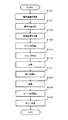
(基板の計測と位置決め方法)
次に、図9に基づき、本実施の形態における基板位置決め方法について説明する。本実施の形態における基板の計測と位置決め方法は、図7及び図8に示す本実施の形態における基板位置決め装置を用いて行うものである。
(Substrate measurement and positioning method)
Next, a substrate positioning method in the present embodiment will be described based on FIG. The substrate measurement and positioning method in the present embodiment is performed using the substrate positioning apparatus in the present embodiment shown in FIGS.
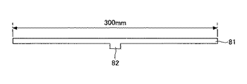
最初に、ステップ102(S102)において、基準基板を回転部40の真空チャック部44上に載置する。具体的には、図10に示すように、基準基板81は、直径が300mmの円形に形成されており、基準基板81の中心部分に凸部82が形成されている。また、真空チャック部44の表面の回転中心41となる部分には、凸部82に対応する不図示の凹部が設けられており、真空チャック部44の凹部に基準基板81の凸部82を挿入することにより、回転部40の回転中心41と基準基板81の中心とが一致するように形成されている。即ち、基準基板81において、回転部40の回転中心41から周囲までの距離が均一となるように形成されている。尚、本実施の形態では、基準基板81の中心部分には凸部82を設け、真空チャック部44には凹部を設けた構成について説明したが、基準基板81を真空チャック部44上に設置した際に、回転部40の回転中心41と基準基板81の中心とが一致するように、基準基板81を設置することができる構成及び方法であれば、他の形状や方法であってもよい。
First, in step 102 (S102), the reference substrate is placed on the
次に、ステップ104(S104)において、基準位置の決定を行う。具体的には、真空チャック部44に基準基板81を載置した状態で、第1の位置決め機構部10及び第2の位置決め機構部20により、基準基板81を基準として第1の位置決め機構部10及び第2の位置決め機構部20の基準位置を決定する。この基準位置の決定は、以下の工程により行う。
Next, in step 104 (S104), a reference position is determined. Specifically, in a state where the
第1の位置決め機構部10では、第1の駆動部13により、第1の基準部11を回転部40の回転中心41に向かう方向に、基準基板81に接触するまで移動させる。この際、第1の基準部11はピン15を中心に回動し、V字状に形成された接触面14が、基準基板81と2点において接触するように調整する。そして、その状態で第1の基準部11と支持部12とを、ネジ16で固定する。第1の位置決め機構部10の基準位置は、回転部40の回転中心41に向かう方向において、第1の基準部11が基準基板81と2点において接触する位置に決定される。また、第2の位置決め機構部20では、第2の駆動部23により、第2の基準部21を回転部40の回転中心41に向かう方向に移動させ、第2の基準部21における接触部24が基準基板81に接触した後、位置センサ28が検出する可動部25までの距離が予め決められた基準の距離、例えば1mmになるようにする。第2の位置決め機構部20の基準位置は、この可動部25までの距離が予め決められた基準の距離になる位置に決定される。この後、第1の位置決め機構部10において、第1の駆動部13により第1の基準部11を基準基板81より離れる方向に移動させ、同様に、第2の位置決め機構部20において、第2の駆動部23により第2の基準部21を基準基板81より離れる方向に移動させる。さらに、この後、基準基板81を真空チャック部44に設けられた凹部より取外す。
In the first
次に、ステップ106(S106)において、基準位置の情報が記憶される。具体的には、ステップ104において決定された第1の位置決め機構部10の基準位置と第2の位置決め機構部20の基準位置を制御部50内に設けられている記憶部52に記憶させる。
Next, in step 106 (S106), the reference position information is stored. Specifically, the reference position of the first
次に、ステップ108(S108)において、基板30を真空チャック部44上に載置する。具体的には、基板30を真空チャック部44上に載置した状態で、真空チャック部44から基板30に向けて窒素ガスを供給し、窒素ガスブローにより基板30を真空チャック部44上において浮上させる。基板30の真空チャック部44に対する面が平坦であるため、真空チャック部44上に載置した状態で、真空チャック部44に吸着してしまう場合があり、この状態での吸着を避けるため、窒素ガスブローを行う。これにより基板30を真空チャック部44上で容易に移動させることができる。このため、この状態では、基板30は真空チャック部44には吸着されていない。尚、この窒素ガスブローは必要に応じて行われるものであり、窒素ガスブローを行うことなく本実施の形態における位置決めを行うことは可能である。
Next, in step 108 (S108), the
次に、ステップ110(S110)において、基板30の計測を行う。具体的には、最初に、第1の基準部11をドレインカップ110とトッププレート120の間に進入させ、第1の位置決め機構部10の基準位置まで第1の駆動部13により移動させる。この際、真空チャック部44に載置された基板30が300mmよりも大きい場合や載置された位置がずれている場合には、第1の基準部11の接触面14が基板30の側面と接触し、第1の基準部11により基板30は押されて第2の位置決め機構部20側に移動する。一方、真空チャック部44に載置された基板30が300mmよりも小さい場合には、基準基板と同条件で載置されると通常は第1の基準部11の接触面14と基板30の側面とは接触することなく、第1の基準部11の接触面14と基板30の側面との間に隙間が形成される。
Next, in step 110 (S110), the
次に、第2の基準部21をドレインカップ110とトッププレート120の間に進入させ、第2の位置決め機構部20の基準位置まで第2の駆動部23により移動させる。この際、第2の基準部21の接触部24と基板30の側面とが接触し、接触部24は回転中心41から離れる方向に押し込まれる。接触部24が押し込まれるのと共に、可動部25も回転中心41から離れる方向に移動する。真空チャック部44に載置された基板30が300mmよりも大きい場合には、位置センサ28により検出される可動部25までの距離は、予め決められた基準の距離である1mmよりも小さくなる。一方、真空チャック部44に載置された基板30が300mmよりも小さい場合には、位置センサ28により検出される可動部25までの距離は、予め決められた基準の距離である1mmよりも大きくなる。これら各々の状態において、位置センサ28により検出された可動部25までの距離を演算部53へ送る。
Next, the
次に、ステップ112(S112)において、位置センサ28により検出された可動部25までの距離に基づき基板30の直径の実測値を制御部50内に設けられている演算部53において算出する。具体的には、基準位置は可動部25までの距離が1mmとなる位置であるため、位置センサ28で検出された距離が0.8mmである場合には、基板30の直径の実測値は300.2mmであるものと算出される。また、位置センサ28で検出された距離が1.2mmである場合には、基板30の直径の実測値は299.8mmであるものと算出される。
Next, in step 112 (S112), the measured value of the diameter of the
尚、第2の基準部21を所定の位置まで移動させた場合に、検出値が大きく外れる場合がある。このような場合としては、接触部24が基板30の側面に形成されたノッチ等に接触している場合が考えられる。このため、このような場合には、ノッチが形成されている位置を避けて基板30の計測を行う必要があるため、回転部40により基板30を90°回転させて、再度、同様の計測を行う。数回行っても、検出値が大きく外れる場合には、真空チャック部44に載置された基板30は所定の規格を満たしていないものと考えられるため、真空チャック部44より取り除き、次の基板30を載置し、ステップ108以降のプロセスを行う。
Note that when the
次に、ステップ114(S114)において、基板30の中心を回転中心41に合わせる補正をするための補正値を演算部53において算出する。即ち、ステップ112において算出した基板30の直径の実測値をもとに、真空チャック部44上に載置されている基板30を現状の位置より移動させる距離となる補正値を算出する。具体的には、ステップ112において、300.2mmと算出された場合には、基準基板81よりも0.2mm大きいため、補正値は+0.2mmの半分の+0.1mmとなる。また、299.8mmと算出された場合には、基準基板81よりも0.2mm小さいため、補正値は−0.2mmの半分の−0.1mmとなる。
Next, in step 114 (S114), the
次に、ステップ116(S116)において、実測値及び補正値についての情報を駆動制御部51に送信する。具体的には、送信部54により駆動制御部51に基板の実測値及び補正値についての情報を送信する。
Next, in step 116 (S116), information about the actual measurement value and the correction value is transmitted to the
次に、ステップ118(S118)において、ステップ116で送信された補正値に基づいて駆動制御部51が真空チャック部44上に載置されている基板30の位置補正を行う。具体的には、補正値が、+0.1mmの場合、基板30の中心は回転部40の回転中心41よりも、第2の位置決め機構部20側に0.1mmずれているため、駆動制御部51が、第1の位置決め機構部10の第1の駆動部13により、第1の基準部11を回転中心41より離れる方向に、0.1mm移動させる。これにより、基板30は第2の基準部21におけるバネ部26により、連結部29と接触部24を介し第1の位置決め機構部10側に押され、基板30の中心と回転中心41とが一致した状態とすることができる。また、補正値が、−0.1mmの場合、基板30の中心は回転部40の回転中心41よりも、第1の位置決め機構部10側に0.1mmずれているため、駆動制御部51が、第1の位置決め機構部10の第1の駆動部13により、第1の基準部11を回転中心41に近づく方向に、0.1mm移動させる。これにより、基板30の側面が第1の基準部11の接触面14を介して押され、第2の位置決め機構部20におけるバネ部26が縮むため、基板30を第2の位置決め機構部20側に移動させることができ、これにより基板30の中心と回転中心41とが一致した状態とすることができる。
Next, in step 118 (S118), the
次に、ステップ120(S120)において、基板30を真空チャック部44に吸着させる。具体的には、ステップ118において、基板30の中心と回転部40における回転中心とが一致している状態となった後、窒素ガスのブローを停止し、真空チャック部44に接続されている真空ポンプ等により排気を行い真空チャック部44に設けられた気体開口部47を介し基板30を真空チャック部44に吸着させる。この後、第1の位置決め機構部10において、第1の駆動部13により、第1の基準部11を回転中心41より離れる方向に移動させることにより、基板30の側面と第1の基準部11の接触面14とが接触していない状態とし、ドレインカップ110の外側に退避させる。同様に、第2の位置決め機構部20において、第2の駆動部23により、第2の基準部21を回転中心41より離れる方向に移動させることにより、基板30の側面と第2の基準部21の接触部24とが接触していない状態し、ドレインカップ110の外側に退避させる。
Next, in step 120 (S120), the
これにより、基板30の中心と回転部40の回転中心41とが一致した状態で真空チャック部44に基板30を吸着させることができる。
Accordingly, the
この後、ドレインカップ110とトッププレート120を閉じて、処理空間を形成する。その処理空間内において、回転部40により基板30を回転させて、各種の基板処理等が行われる。そして、基板30の処理等を行った後は、ドレインカップ110とトッププレート120を離間させ、真空チャック部44において基板30の真空チャックを解除し、基板30を真空チャック部44より取外す。
Thereafter, the
本実施の形態では、回転中心41と基板30の中心とが一致しているため、回転中心41から基板の端部までの距離を均一にすることができる。
In the present embodiment, since the
本実施の形態における基板位置決め装置及び基板位置決め方法は、基板のべベル処理を行う装置、基板の中心から周囲に向けての処理を行う装置、基板の周囲から中心に向けての処理を行う装置等に用いることが可能である。 The substrate positioning apparatus and the substrate positioning method in the present embodiment are a device that performs bevel processing of a substrate, a device that performs processing from the center of the substrate toward the periphery, and a device that performs processing from the periphery of the substrate toward the center. Etc. can be used.
また、ウエハ等の基板を回転させて処理を行う基板処理装置の場合においては、特に、大型の基板の処理を行う場合、基板の中心と回転中心とが一致していないと、偏心により所望の回転をさせることができず、所望の処理を行うことができない場合がある。このような場合においても、本実施の形態における基板位置決め装置及び基板位置決め方法を適用することができる。 Also, in the case of a substrate processing apparatus that performs processing by rotating a substrate such as a wafer, particularly when processing a large substrate, if the center of the substrate does not coincide with the center of rotation, a desired result is obtained due to eccentricity. In some cases, the rotation cannot be performed and a desired process cannot be performed. Even in such a case, the substrate positioning apparatus and the substrate positioning method in the present embodiment can be applied.
尚、基準基板81を用いた基準位置検出工程は一度行えばよいため、ステップ108からステップ120の工程を繰り返すことにより、複数の基板に対して中心位置の正確な位置決めを短時間に行うことが可能である。
Since the reference position detection process using the
また、上記位置合せ方法については、プログラムとして制御部50における記憶部52または外部記憶部60等に格納されており、このプログラムに基づく自動制御により行うことも可能である。
The alignment method is stored as a program in the
また、図1及び図2に示す基板処理システムにおいては、1つの基板処理ユニット内にある上述した基板位置決め装置により得られた基板30の直径等の実測値及び補正値についての情報を機械制御ユニット213または他の基板処理ユニットに送信し、他の基板処理ユニットにおいて同じ基板の処理を行う場合に、基板30の直径等の実測値及び補正値についての情報を用いて位置決め等を行うことも可能である。
In the substrate processing system shown in FIG. 1 and FIG. 2, information on the actual measurement value and the correction value such as the diameter of the
また、基板処理ユニットとは別個に、基板位置決め装置を備えたユニットを設け、この基板位置決め装置により得られた基板の直径等の実測値及び補正値についての情報を基板処理ユニットに送信してもよい。 In addition, a unit including a substrate positioning device may be provided separately from the substrate processing unit, and information on the actual measurement value and the correction value such as the diameter of the substrate obtained by the substrate positioning device may be transmitted to the substrate processing unit. Good.
具体的には、図11に示すように、ウエハ受け渡しユニット214内等に基板位置決め装置を設置し、この基板位置決め装置により得られた基板の直径等の実測値及び補正値についての情報を送信部290よりその基板の処理を行う基板処理ユニット271〜274に送信する。これにより、送信されてきた基板の直径等の実測値および補正値についての情報に基づき、基板の中心と回転中心を合わせる位置決めや基板処理を行うためのノズル位置の調整を行うことができる。また、基板位置決め装置により得られた基板の直径等の実測値及び補正値についての情報を送信部290より機械制御ユニット213に送信した場合、機械制御ユニット213から基板処理ユニット271〜274に送信してもよい。
Specifically, as shown in FIG. 11, a substrate positioning device is installed in the
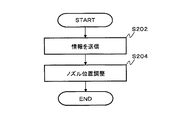
これらの場合における基板処理方法について、図12に基づき説明する。 The substrate processing method in these cases will be described with reference to FIG.
最初に、ステップ202(S202)において、基板位置決め装置により得られた基板の直径等の実測値及び補正値についての情報を送信部290により、機械制御ユニット213または基板処理ユニット271〜274に送信する。尚、機械制御ユニット213の送信された場合には、さらに、機械制御ユニット213より基板処理ユニット271〜274に送信される。
First, in step 202 (S202), information on the actual measurement value and the correction value such as the diameter of the substrate obtained by the substrate positioning device is transmitted to the
次に、ステップ204(S204)において、例えば、基板処理ユニット271〜274において、基板の直径等の情報を用いて基板処理を行う。具体的には、基板処理ユニット271〜274において基板位置決め装置により得られた基板の直径等の実測値及び補正値についての情報に基づき、基板の中心と回転中心を合わせる位置決めやノズル位置の調整等を行う。この後、ウエハの基板処理が行われる。
Next, in step 204 (S204), for example, the
以上、本発明の実施に係る形態について説明したが、上記内容は、発明の内容を限定するものではない。 As mentioned above, although the form which concerns on implementation of this invention was demonstrated, the said content does not limit the content of invention.
10 第1の位置決め機構部
11 第1の基準部
12 支持部
13 第1の駆動部
14 接触面
15 ピン
16 ネジ
20 第2の位置決め機構部
21 第2の基準部
22 支持部
23 第2の駆動部
24 接触部
25 可動部
26 バネ部
27 本体部
28 位置センサ
29 連結部
30 基板
40 回転部
41 回転中心
44 真空チャック部
50 制御部
51 駆動制御部
52 記憶部
53 演算部
54 送信部
60 外部記憶部
DESCRIPTION OF
Claims (15)
基板載置部と、
前記基板の側面と2点以上で接触させる第1の基準部を有する第1の位置決め機構部と、
前記第1の位置決め機構部を駆動させる第1の駆動部と、
接触部において前記基板の側面に接触する第2の基準部と、前記接触部に対し前記第1の駆動部の移動方向に力を加えることのできる弾性部と、前記第2の基準部の位置情報を検出するための検出部とを有する第2の位置決め機構部と、
前記第2の位置決め機構部を駆動させる第2の駆動部と、
前記第1の駆動部及び前記第2の駆動部を制御する制御部と、
を有し、
前記第1の基準部と前記第2の基準部は、前記基板載置部の中心が存在する同一線上に配置されており、
前記制御部は、前記第1の駆動部と第2の駆動部を制御して、前記第1の位置決め機構部及び前記第2の位置決め機構部を予め決められた基準位置まで移動させることにより、前記第1の基準部と前記基板の側面とを接触させ、さらに、前記第2の基準部と前記基板の側面とを接触させた後、前記検出部によって検出された位置情報に基づいて、前記基板の位置決めを行うことを特徴とする基板位置決め装置。 In a substrate positioning device for positioning a substrate,
A substrate mounting unit;
A first positioning mechanism having a side surface and a first reference portion Ru contacted with two or more points of the substrate,
A first drive section for driving the first positioning mechanism section;
A second reference portion that contacts the side surface of the substrate at the contact portion; an elastic portion that can apply a force to the contact portion in the moving direction of the first drive portion; and a position of the second reference portion. A second positioning mechanism having a detector for detecting information ;
A second drive section for driving the second positioning mechanism section;
A control unit for controlling the first driving unit and the second driving unit ;
Have
The first reference part and the second reference part are arranged on the same line where the center of the substrate mounting part exists,
The control unit controls the first drive unit and the second drive unit to move the first positioning mechanism unit and the second positioning mechanism unit to a predetermined reference position, Based on the positional information detected by the detection unit, after contacting the first reference portion and the side surface of the substrate, and further contacting the second reference portion and the side surface of the substrate, board positioning device, characterized in that for positioning the substrate.
前記接触部は、円形を有する形状であって、前記連結部に前記円形の中心を軸として回転可能な状態で取り付けられているものであって、前記基板とは一点で接触するものであることを特徴とする請求項1に記載の基板位置決め装置。 The second reference part includes a main body part to which the elastic part and the detection part are connected, and a connecting part that connects the elastic part and the contact part,
The contact portion has a circular shape, and is attached to the connecting portion so as to be rotatable around the center of the circle, and is in contact with the substrate at a single point. The substrate positioning apparatus according to claim 1.
前記制御部は、前記検出部によって検出された前記位置情報と前記基準位置情報との差を算出することにより前記基板の直径を算出し、前記基板の直径に基づき前記第1の位置決め機構部の位置を移動させて位置決めを行うことを特徴とする請求項1または2に記載の基板位置決め装置。 A storage unit for storing reference position information of the first positioning mechanism unit and the second positioning mechanism unit with respect to a reference substrate used as a reference when positioning;
The control unit calculates a diameter of the substrate by calculating a difference between the position information detected by the detection unit and the reference position information. Based on the diameter of the substrate, the control unit the substrate positioning apparatus according to claim 1 or 2 position by moving the and performs positioning.
請求項1から5のいずれかに記載の基板位置決め装置と、を備え
前記基板位置決め装置は、前記下部カップと前記プレートの間に進入して位置決めを行い、位置決め終了後は前記下部カップの外側に退避することを特徴とする基板処理装置。 A substrate processing unit for processing the substrate, comprising: a lower cup surrounding the substrate mounting unit; and a plate covering an opening of the lower cup;
A substrate positioning device according to any one of claims 1 to 5 , wherein the substrate positioning device enters between the lower cup and the plate to perform positioning, and after positioning is located outside the lower cup. A substrate processing apparatus which is retracted.
前記基板載置部上に基板を載置する基板載置工程と、
第1の位置決め機構部及び第2の位置決め機構部を予め決められた基準位置まで移動させる移動工程と、
前記基準位置において、前記基板の側面を第1の位置決め機構部における第1の基準部の接触面に接触させ、さらに、第2の位置決め機構部における第2の基準部の接触部に接触させた後、前記検出部により前記基板の位置を検出する検出工程と、
前記検出された位置情報に基づいて、前記基板の位置決めを行う基板位置決め工程と、
を有することを特徴とする基板位置決め方法。 A first positioning mechanism portion having a first reference portion that is in contact with the side surface of the substrate at two or more points; a second reference portion that is in contact with the side surface of the substrate at the contact portion; A second positioning mechanism having an elastic part capable of applying a force in the moving direction of the driving part and a detection part for detecting position information of the second reference part. In the substrate positioning method, wherein the reference portion and the second reference portion are arranged on the same line where the center of the substrate mounting portion exists ,
A substrate placing step of placing the substrate on the substrate mounting portion,
A moving step of moving the first positioning mechanism part and the second positioning mechanism part to a predetermined reference position;
At the reference position, the side surface of the substrate is brought into contact with the contact surface of the first reference portion in the first positioning mechanism portion, and is further brought into contact with the contact portion of the second reference portion in the second positioning mechanism portion . And a detection step of detecting the position of the substrate by the detection unit ;
Based on the detected position information, and the substrate positioning step for positioning the substrate,
A substrate positioning method characterized by comprising:
基準となる大きさで形成された基準基板を前記基板載置部の中心と前記基準基板の中心とが一致するように、前記基板載置部上に載置する基準基板載置工程と、
前記第1の基準部の前記接触面と前記基準基板とを接触させ、前記第2の基準部の前記接触部と前記基準基板とを接触させることにより、前記第1の位置決め機構部と前記第2の位置決め機構部の前記基準位置を決定する基準位置決定工程と、
前記基準位置決定工程で決定された前記基準位置を記憶する記憶工程と、
を有することを特徴とする請求項7から10のいずれかに記載の基板位置決め方法。 Before the substrate placing process,
A reference substrate placement step of placing a reference substrate formed in a reference size on the substrate placement portion so that the center of the substrate placement portion and the center of the reference substrate coincide with each other;
By bringing the contact surface of the first reference portion into contact with the reference substrate and bringing the contact portion in the second reference portion into contact with the reference substrate, the first positioning mechanism portion and the first substrate A reference position determining step for determining the reference position of the two positioning mechanisms;
A storage step of storing the reference position determined in the reference position determination step;
Board positioning method according to any one of claims 7 to 10, characterized in that it has a.
前記計測された前記基板の直径と、基準基板の直径との差を算出する比較工程と、
前記比較工程において得られた差に基づき、前記基板の中心と前記基板載置部の中心とが一致するように補正量を算出する補正量算出工程と、
前記補正量に基づき前記第1の位置決め機構部を移動させることにより、前記基板載置部上において、前記基板を前記補正量移動させる位置補正工程と、
を有することを特徴とする請求項8に記載の基板位置決め方法。 The substrate positioning step includes
The diameter of the measured said substrate, and a comparison step of calculating the difference between the diameter of the criteria substrate,
Based on the difference obtained in the comparison step, a correction amount calculation step for calculating a correction amount so that the center of the substrate and the center of the substrate mounting portion coincide with each other;
A position correction step of moving the substrate by the correction amount on the substrate platform by moving the first positioning mechanism based on the correction amount;
The substrate positioning method according to claim 8 , further comprising:
Computer readable recording medium recording a program for executing a substrate positioning method according to any one of claims 7 14 for the computer.
Priority Applications (5)
| Application Number | Priority Date | Filing Date | Title |
|---|---|---|---|
| JP2011058278A JP5572575B2 (en) | 2010-05-12 | 2011-03-16 | Substrate positioning apparatus, substrate processing apparatus, substrate positioning method, and storage medium storing program |
| KR1020110032787A KR101599086B1 (en) | 2010-05-12 | 2011-04-08 | Apparatus for determining position of substrate, apparatus for processing substrates, method for determining position of substrate, and storage medium recording program |
| TW100115790A TWI509728B (en) | 2010-05-12 | 2011-05-05 | Substrate positioning device, substrate processing device, substrate positioning method, and memory medium with recorded program |
| US13/104,374 US9008817B2 (en) | 2010-05-12 | 2011-05-10 | Substrate positioning apparatus, substrate processing apparatus, substrate positioning method, and computer readable medium having a program stored thereon |
| CN201110125137.6A CN102244026B (en) | 2010-05-12 | 2011-05-12 | Base positioner, substrate board treatment and substrate positioning method |
Applications Claiming Priority (3)
| Application Number | Priority Date | Filing Date | Title |
|---|---|---|---|
| JP2010110366 | 2010-05-12 | ||
| JP2010110366 | 2010-05-12 | ||
| JP2011058278A JP5572575B2 (en) | 2010-05-12 | 2011-03-16 | Substrate positioning apparatus, substrate processing apparatus, substrate positioning method, and storage medium storing program |
Publications (3)
| Publication Number | Publication Date |
|---|---|
| JP2011258924A JP2011258924A (en) | 2011-12-22 |
| JP2011258924A5 JP2011258924A5 (en) | 2013-04-04 |
| JP5572575B2 true JP5572575B2 (en) | 2014-08-13 |
Family
ID=44912452
Family Applications (1)
| Application Number | Title | Priority Date | Filing Date |
|---|---|---|---|
| JP2011058278A Active JP5572575B2 (en) | 2010-05-12 | 2011-03-16 | Substrate positioning apparatus, substrate processing apparatus, substrate positioning method, and storage medium storing program |
Country Status (5)
| Country | Link |
|---|---|
| US (1) | US9008817B2 (en) |
| JP (1) | JP5572575B2 (en) |
| KR (1) | KR101599086B1 (en) |
| CN (1) | CN102244026B (en) |
| TW (1) | TWI509728B (en) |
Cited By (1)
| Publication number | Priority date | Publication date | Assignee | Title |
|---|---|---|---|---|
| US10727090B2 (en) | 2017-05-31 | 2020-07-28 | SCREEN Holdings Co., Ltd. | Substrate processing apparatus and substrate processing method |
Families Citing this family (22)
| Publication number | Priority date | Publication date | Assignee | Title |
|---|---|---|---|---|
| JP5449239B2 (en) * | 2010-05-12 | 2014-03-19 | 東京エレクトロン株式会社 | Substrate processing apparatus, substrate processing method, and storage medium storing program |
| JP5243491B2 (en) * | 2010-06-18 | 2013-07-24 | 東京エレクトロン株式会社 | Positioning apparatus, substrate processing apparatus, and reference member fixing method |
| JP5727244B2 (en) * | 2011-01-28 | 2015-06-03 | リンテック株式会社 | Support apparatus and support method |
| JP5996381B2 (en) * | 2011-12-28 | 2016-09-21 | 東京エレクトロン株式会社 | Substrate processing apparatus and substrate processing method |
| JP5835188B2 (en) * | 2012-11-06 | 2015-12-24 | 東京エレクトロン株式会社 | Method for removing coating film on peripheral edge of substrate, substrate processing apparatus, and storage medium |
| CN103594406B (en) * | 2013-11-05 | 2016-08-24 | 中国电子科技集团公司第四十五研究所 | Self-centering positioning chuck and centering positioning method for semiconductor wafer |
| TWI668795B (en) | 2014-09-15 | 2019-08-11 | 美商瓦里安半導體設備公司 | Active substrate alignment system for semiconductor processing and method for aligning substrate |
| JP6475756B2 (en) * | 2015-02-04 | 2019-02-27 | 川崎重工業株式会社 | Robot shake automatic adjustment device and robot shake automatic adjustment method |
| JP6612670B2 (en) * | 2016-03-31 | 2019-11-27 | 東京応化工業株式会社 | Substrate processing apparatus and substrate processing method |
| CN108242417B (en) * | 2016-12-26 | 2020-10-16 | 北京北方华创微电子装备有限公司 | Manual silicon chip conveying mechanism |
| JP6920849B2 (en) * | 2017-03-27 | 2021-08-18 | 株式会社荏原製作所 | Substrate processing method and equipment |
| CN111217149B (en) * | 2018-11-23 | 2024-08-27 | 合肥欣奕华智能机器股份有限公司 | Substrate calibration device, substrate calibration method and substrate conveying device |
| CN114341398B (en) | 2019-08-23 | 2024-10-29 | 朗姆研究公司 | Temperature controlled chandelier type sprinkler |
| JP7426808B2 (en) | 2019-11-27 | 2024-02-02 | 株式会社Screenホールディングス | Substrate processing equipment |
| JP7637686B2 (en) * | 2020-01-06 | 2025-02-28 | ラム リサーチ コーポレーション | Showerhead with faceplate having internal contour - Patents.com |
| JP2022048506A (en) * | 2020-09-15 | 2022-03-28 | 株式会社ダイヘン | Aligner device |
| CN113634401A (en) * | 2021-09-08 | 2021-11-12 | 江苏科环新材料有限公司 | Nano metal coating processingequipment |
| CN114446848B (en) * | 2021-12-28 | 2025-06-24 | 苏州精濑光电有限公司 | Auxiliary positioning mechanism of material box |
| JP7813152B2 (en) | 2022-02-07 | 2026-02-12 | 株式会社Screenホールディングス | Centering device, centering method, and substrate processing apparatus |
| KR102775356B1 (en) * | 2022-12-21 | 2025-03-06 | 세메스 주식회사 | Apparatus and method for treating substrate including eccentricity correction unit |
| KR102898065B1 (en) * | 2023-10-17 | 2025-12-08 | 후쿠무라 코포레이션 | Pyrolysis carbonization treatment device |
| JP7801827B1 (en) * | 2025-09-08 | 2026-01-19 | 株式会社オプトラン | Alignment device and alignment method |
Family Cites Families (36)
| Publication number | Priority date | Publication date | Assignee | Title |
|---|---|---|---|---|
| JPH04274343A (en) * | 1991-03-01 | 1992-09-30 | Fujitsu Ltd | Positioning device for semiconductor wafer and positioning method |
| TW319751B (en) * | 1995-05-18 | 1997-11-11 | Toshiba Co Ltd | |
| JPH1089904A (en) * | 1996-09-17 | 1998-04-10 | Hitachi Electron Eng Co Ltd | V-notch wafer positioning device |
| JP4547524B2 (en) * | 2000-12-05 | 2010-09-22 | 川崎重工業株式会社 | Work processing method, work processing apparatus and robot |
| JP4389424B2 (en) * | 2001-12-25 | 2009-12-24 | 東京エレクトロン株式会社 | To-be-processed object conveyance mechanism and processing system |
| JP4173309B2 (en) * | 2002-01-28 | 2008-10-29 | 東京エレクトロン株式会社 | Centering device and single wafer inspection device |
| US20030168175A1 (en) * | 2002-03-08 | 2003-09-11 | Kim Kyung-Tae | Substrate alignment apparatus |
| JP3956350B2 (en) * | 2002-03-25 | 2007-08-08 | 東京エレクトロン株式会社 | Substrate processing apparatus having positioning function and substrate processing method having positioning function |
| US6700090B2 (en) * | 2002-04-26 | 2004-03-02 | Hitachi High-Technologies Corporation | Plasma processing method and plasma processing apparatus |
| US7367773B2 (en) * | 2002-05-09 | 2008-05-06 | Maxtor Corporation | Apparatus for combining or separating disk pairs simultaneously |
| US7499767B2 (en) * | 2003-02-20 | 2009-03-03 | Applied Materials, Inc. | Methods and apparatus for positioning a substrate relative to a support stage |
| JP2004342939A (en) | 2003-05-16 | 2004-12-02 | Shimada Phys & Chem Ind Co Ltd | Substrate processing equipment |
| JP4304692B2 (en) * | 2003-06-27 | 2009-07-29 | ローツェ株式会社 | Clamp device for checking the gripping of a disk-shaped object |
| WO2005055312A1 (en) * | 2003-12-04 | 2005-06-16 | Hirata Corporation | Substrate positioning system |
| KR101003666B1 (en) * | 2003-12-10 | 2010-12-23 | 엘지디스플레이 주식회사 | Aligner |
| US7824498B2 (en) * | 2004-02-24 | 2010-11-02 | Applied Materials, Inc. | Coating for reducing contamination of substrates during processing |
| JP2005262367A (en) * | 2004-03-18 | 2005-09-29 | Tokyo Electron Ltd | Method and apparatus for checking transfer deviation of transfer robot |
| JP4502199B2 (en) * | 2004-10-21 | 2010-07-14 | ルネサスエレクトロニクス株式会社 | Etching apparatus and etching method |
| US7547181B2 (en) * | 2004-11-15 | 2009-06-16 | Dainippon Screen Mfg. Co., Ltd. | Substrate position correcting method and apparatus using either substrate radius or center of rotation correction adjustment sum |
| US20090017733A1 (en) * | 2005-04-19 | 2009-01-15 | Ebara Corporation | Substrate processing apparatus |
| JP4892225B2 (en) * | 2005-10-28 | 2012-03-07 | 株式会社日立ハイテクノロジーズ | Vacuum processing method, vacuum transfer apparatus, and semiconductor processing apparatus |
| JP4657090B2 (en) | 2005-11-17 | 2011-03-23 | 大日本スクリーン製造株式会社 | Substrate processing equipment |
| JP4781802B2 (en) * | 2005-12-06 | 2011-09-28 | 東京応化工業株式会社 | Support plate laminating means and laminating apparatus, and support plate laminating method |
| JP4698407B2 (en) * | 2005-12-20 | 2011-06-08 | 大日本スクリーン製造株式会社 | Substrate processing apparatus and substrate processing method |
| JP4961895B2 (en) * | 2006-08-25 | 2012-06-27 | 東京エレクトロン株式会社 | Wafer transfer device, wafer transfer method, and storage medium |
| JP5030542B2 (en) * | 2006-11-10 | 2012-09-19 | 株式会社日立ハイテクノロジーズ | Vacuum processing equipment |
| JP2008173744A (en) * | 2007-01-22 | 2008-07-31 | Tokyo Electron Ltd | Transport position adjustment method of transport system |
| US20090110532A1 (en) * | 2007-10-29 | 2009-04-30 | Sokudo Co., Ltd. | Method and apparatus for providing wafer centering on a track lithography tool |
| JP2009130011A (en) | 2007-11-21 | 2009-06-11 | Atel Corp | Substrate positioning device |
| JP5435861B2 (en) * | 2007-12-13 | 2014-03-05 | 芝浦メカトロニクス株式会社 | Electronic component mounting apparatus and mounting method |
| JP4926933B2 (en) * | 2007-12-14 | 2012-05-09 | 東京エレクトロン株式会社 | Substrate cleaning apparatus and substrate cleaning method |
| US7963736B2 (en) * | 2008-04-03 | 2011-06-21 | Asm Japan K.K. | Wafer processing apparatus with wafer alignment device |
| JP5301505B2 (en) * | 2009-08-27 | 2013-09-25 | 東京エレクトロン株式会社 | Liquid processing apparatus and liquid processing method |
| JP5449239B2 (en) * | 2010-05-12 | 2014-03-19 | 東京エレクトロン株式会社 | Substrate processing apparatus, substrate processing method, and storage medium storing program |
| JP5243491B2 (en) * | 2010-06-18 | 2013-07-24 | 東京エレクトロン株式会社 | Positioning apparatus, substrate processing apparatus, and reference member fixing method |
| JP5729326B2 (en) * | 2012-02-14 | 2015-06-03 | 東京エレクトロン株式会社 | Liquid processing apparatus, liquid processing method, and storage medium |
-
2011
- 2011-03-16 JP JP2011058278A patent/JP5572575B2/en active Active
- 2011-04-08 KR KR1020110032787A patent/KR101599086B1/en active Active
- 2011-05-05 TW TW100115790A patent/TWI509728B/en active
- 2011-05-10 US US13/104,374 patent/US9008817B2/en active Active
- 2011-05-12 CN CN201110125137.6A patent/CN102244026B/en active Active
Cited By (1)
| Publication number | Priority date | Publication date | Assignee | Title |
|---|---|---|---|---|
| US10727090B2 (en) | 2017-05-31 | 2020-07-28 | SCREEN Holdings Co., Ltd. | Substrate processing apparatus and substrate processing method |
Also Published As
| Publication number | Publication date |
|---|---|
| JP2011258924A (en) | 2011-12-22 |
| CN102244026A (en) | 2011-11-16 |
| US20110282484A1 (en) | 2011-11-17 |
| TW201205712A (en) | 2012-02-01 |
| KR20110125166A (en) | 2011-11-18 |
| CN102244026B (en) | 2016-04-20 |
| KR101599086B1 (en) | 2016-03-14 |
| US9008817B2 (en) | 2015-04-14 |
| TWI509728B (en) | 2015-11-21 |
Similar Documents
| Publication | Publication Date | Title |
|---|---|---|
| JP5572575B2 (en) | Substrate positioning apparatus, substrate processing apparatus, substrate positioning method, and storage medium storing program | |
| JP5449239B2 (en) | Substrate processing apparatus, substrate processing method, and storage medium storing program | |
| US9799540B2 (en) | Liquid processing apparatus, liquid processing method and storage medium | |
| JP6363605B2 (en) | System and method for automatically correcting rotational misalignment of a wafer on a film frame | |
| CN110050336B (en) | Wafer edge lift pin design for manufacturing semiconductor devices | |
| KR101423811B1 (en) | A positiong apparatus, a substrate processing apparatus and method for fixing a reference member | |
| US20150044008A1 (en) | Robot Blade Design | |
| US20090092470A1 (en) | End effector with sensing capabilities | |
| TWI839869B (en) | Substrate processing device and substrate processing method | |
| CN216980525U (en) | Wafer alignment device | |
| JP6756600B2 (en) | Substrate processing equipment and substrate processing method | |
| JP7791053B2 (en) | Nozzle position adjusting method and substrate processing apparatus | |
| US20250014917A1 (en) | Separating apparatus, separating system and separating method | |
| US20250012606A1 (en) | Distance measuring device, distance measuring method, bonding apparatus, and bonding method | |
| US20250014916A1 (en) | Separating apparatus, separating system and separating method | |
| JP2025042743A (en) | Centering device, centering method, and substrate processing apparatus | |
| KR100686453B1 (en) | Semiconductor Wafer Pod | |
| JP2024164427A (en) | Bonding device, bonding system, and bonding method | |
| JP2024106617A (en) | Centering device, centering method, and substrate processing apparatus | |
| KR20050037828A (en) | Calibration device of wafer transfer robot |
Legal Events
| Date | Code | Title | Description |
|---|---|---|---|
| A521 | Request for written amendment filed |
Free format text: JAPANESE INTERMEDIATE CODE: A523 Effective date: 20130218 |
|
| A621 | Written request for application examination |
Free format text: JAPANESE INTERMEDIATE CODE: A621 Effective date: 20130218 |
|
| A977 | Report on retrieval |
Free format text: JAPANESE INTERMEDIATE CODE: A971007 Effective date: 20131216 |
|
| A131 | Notification of reasons for refusal |
Free format text: JAPANESE INTERMEDIATE CODE: A131 Effective date: 20140107 |
|
| A521 | Request for written amendment filed |
Free format text: JAPANESE INTERMEDIATE CODE: A523 Effective date: 20140303 |
|
| TRDD | Decision of grant or rejection written | ||
| A01 | Written decision to grant a patent or to grant a registration (utility model) |
Free format text: JAPANESE INTERMEDIATE CODE: A01 Effective date: 20140603 |
|
| A61 | First payment of annual fees (during grant procedure) |
Free format text: JAPANESE INTERMEDIATE CODE: A61 Effective date: 20140630 |
|
| R150 | Certificate of patent or registration of utility model |
Ref document number: 5572575 Country of ref document: JP Free format text: JAPANESE INTERMEDIATE CODE: R150 |
|
| R250 | Receipt of annual fees |
Free format text: JAPANESE INTERMEDIATE CODE: R250 |
|
| R250 | Receipt of annual fees |
Free format text: JAPANESE INTERMEDIATE CODE: R250 |
|
| R250 | Receipt of annual fees |
Free format text: JAPANESE INTERMEDIATE CODE: R250 |
|
| R250 | Receipt of annual fees |
Free format text: JAPANESE INTERMEDIATE CODE: R250 |
|
| R250 | Receipt of annual fees |
Free format text: JAPANESE INTERMEDIATE CODE: R250 |
|
| R250 | Receipt of annual fees |
Free format text: JAPANESE INTERMEDIATE CODE: R250 |
|
| R250 | Receipt of annual fees |
Free format text: JAPANESE INTERMEDIATE CODE: R250 |