JP5570743B2 - 半導体装置 - Google Patents
半導体装置 Download PDFInfo
- Publication number
- JP5570743B2 JP5570743B2 JP2009055339A JP2009055339A JP5570743B2 JP 5570743 B2 JP5570743 B2 JP 5570743B2 JP 2009055339 A JP2009055339 A JP 2009055339A JP 2009055339 A JP2009055339 A JP 2009055339A JP 5570743 B2 JP5570743 B2 JP 5570743B2
- Authority
- JP
- Japan
- Prior art keywords
- layer
- substrate
- conductivity type
- diffusion layer
- semiconductor
- Prior art date
- Legal status (The legal status is an assumption and is not a legal conclusion. Google has not performed a legal analysis and makes no representation as to the accuracy of the status listed.)
- Active
Links
- 239000004065 semiconductor Substances 0.000 title claims description 66
- 239000000758 substrate Substances 0.000 claims description 54
- 238000009792 diffusion process Methods 0.000 claims description 42
- 239000012535 impurity Substances 0.000 claims description 26
- 238000002955 isolation Methods 0.000 claims description 18
- BOTDANWDWHJENH-UHFFFAOYSA-N Tetraethyl orthosilicate Chemical compound CCO[Si](OCC)(OCC)OCC BOTDANWDWHJENH-UHFFFAOYSA-N 0.000 claims description 12
- 239000011810 insulating material Substances 0.000 claims description 4
- 229910021420 polycrystalline silicon Inorganic materials 0.000 claims description 4
- 229920005591 polysilicon Polymers 0.000 claims description 4
- 238000002598 diffusion tensor imaging Methods 0.000 description 31
- 238000010586 diagram Methods 0.000 description 12
- 230000015556 catabolic process Effects 0.000 description 9
- 239000000463 material Substances 0.000 description 7
- 238000002513 implantation Methods 0.000 description 6
- 238000000034 method Methods 0.000 description 6
- 238000004088 simulation Methods 0.000 description 6
- 230000003071 parasitic effect Effects 0.000 description 3
- 230000001133 acceleration Effects 0.000 description 2
- 230000015572 biosynthetic process Effects 0.000 description 2
- 230000007547 defect Effects 0.000 description 2
- OAICVXFJPJFONN-UHFFFAOYSA-N Phosphorus Chemical compound [P] OAICVXFJPJFONN-UHFFFAOYSA-N 0.000 description 1
- 229910052787 antimony Inorganic materials 0.000 description 1
- WATWJIUSRGPENY-UHFFFAOYSA-N antimony atom Chemical compound [Sb] WATWJIUSRGPENY-UHFFFAOYSA-N 0.000 description 1
- 229910052785 arsenic Inorganic materials 0.000 description 1
- RQNWIZPPADIBDY-UHFFFAOYSA-N arsenic atom Chemical compound [As] RQNWIZPPADIBDY-UHFFFAOYSA-N 0.000 description 1
- 230000006866 deterioration Effects 0.000 description 1
- 230000000694 effects Effects 0.000 description 1
- 230000005684 electric field Effects 0.000 description 1
- 229910021478 group 5 element Inorganic materials 0.000 description 1
- 229910052698 phosphorus Inorganic materials 0.000 description 1
- 239000011574 phosphorus Substances 0.000 description 1
Images


Classifications
-
- H—ELECTRICITY
- H01—ELECTRIC ELEMENTS
- H01L—SEMICONDUCTOR DEVICES NOT COVERED BY CLASS H10
- H01L29/00—Semiconductor devices specially adapted for rectifying, amplifying, oscillating or switching and having potential barriers; Capacitors or resistors having potential barriers, e.g. a PN-junction depletion layer or carrier concentration layer; Details of semiconductor bodies or of electrodes thereof ; Multistep manufacturing processes therefor
- H01L29/66—Types of semiconductor device ; Multistep manufacturing processes therefor
- H01L29/68—Types of semiconductor device ; Multistep manufacturing processes therefor controllable by only the electric current supplied, or only the electric potential applied, to an electrode which does not carry the current to be rectified, amplified or switched
- H01L29/76—Unipolar devices, e.g. field effect transistors
- H01L29/772—Field effect transistors
- H01L29/78—Field effect transistors with field effect produced by an insulated gate
- H01L29/7801—DMOS transistors, i.e. MISFETs with a channel accommodating body or base region adjoining a drain drift region
- H01L29/7816—Lateral DMOS transistors, i.e. LDMOS transistors
Landscapes
- Engineering & Computer Science (AREA)
- Microelectronics & Electronic Packaging (AREA)
- Power Engineering (AREA)
- Physics & Mathematics (AREA)
- Ceramic Engineering (AREA)
- Condensed Matter Physics & Semiconductors (AREA)
- General Physics & Mathematics (AREA)
- Computer Hardware Design (AREA)
- Element Separation (AREA)
- Metal-Oxide And Bipolar Metal-Oxide Semiconductor Integrated Circuits (AREA)
- Insulated Gate Type Field-Effect Transistor (AREA)
Description
まず、一般的なDTI技術を用いた素子分離構造について説明する。図1は、一般的なDTI構造を有する半導体装置の断面構成図である。図1において、第1導電型(例えばP型)の基板1上には、第2導電型(例えばN型)の半導体層であるEPI(エピタキシャル)層2が形成されている。また、基板1とEPI層2とにわたって、N型の埋め込み層3(N型の第1の埋め込み層)が形成されている。
図5は、本実施の形態にかかるDTI構造を有する半導体装置の断面構成図である。図5に示すように、本実施の形態では、DTI17の構成が図2のDTI4の場合と異なっている。すなわち、DTI17は、深いトレンチ25の内壁に沿って形成されたTEOS膜15と、このTEOS膜15を覆うように埋め込まれたポリシリコン16とからなる。なお、図5におけるその他の構成は図2と同様であるので、同一の構成要素には同一の符号を付してその詳細な説明を省略する。
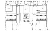
本実施の形態では、第1または第2の実施の形態で説明したDTI構造を、素子領域にDMOS(Diffused MOS)トランジスタが形成された半導体装置に適用するものである。DMOSトランジスタは高耐圧性が要求されるため、対基板耐圧を向上させチップシュリンクも可能な第1または第2の実施の形態のDTI構造の好適な適用例である。
7 埋め込み層、 8 半導体層、 9 半導体層、10 半導体層、11 半導体層 12 埋め込み層、25 トレンチ、26 TEOS膜
Claims (3)
- 第1導電型の基板と、
この基板上に形成された第2導電型の半導体層と、
前記基板と前記半導体層とにわたって形成された第2導電型の第1の埋め込み層と、
この第1の埋め込み層の下に形成され前記第1の埋め込み層よりも不純物濃度の低い第2導電型の第2の埋め込み層と、
前記半導体層上に形成された第2導電型の第1の拡散層と、
この第1の拡散層上に形成され前記第1の拡散層よりも不純物濃度の高いドレイン領域としての第2導電型の第2の拡散層と、
前記半導体層上に形成された第1導電型の第3の拡散層と、
この第3の拡散層上に形成された前記第3の拡散層よりも不純物濃度の高い第1導電型の第4の拡散層と、
前記第3の拡散層上で前記第4の拡散層と隣接して形成されたソース領域としての第2導電型の第5の拡散層と、
前記半導体層の上方に前記第1の拡散層と前記第3の拡散層との間にわたって形成されたゲート膜と、
前記半導体層上であって、前記半導体層、前記第1および第2の埋め込み層、前記第1〜第5の拡散層、ならびに前記ゲート膜を含む素子領域の領域端に形成されて、当該素子領域を素子分離する第1の素子分離領域と、
前記第1の素子分離領域の下に形成され、前記半導体層、前記第1および第2の埋め込み層の側面を囲むように、前記基板内に達し内部に絶縁材料が埋め込まれたトレンチを備えてなる第2の素子分離領域と、
前記素子領域の外部では、前記基板と前記半導体層とにわたって形成された第1導電型の第3の埋め込み層と、この第3の埋め込み層上に形成され前記基板よりも不純物濃度の低い第1導電型の第1の半導体層と、この第1の半導体層上に形成され前記基板よりも不純物濃度の高い第1導電型の第2の半導体層と、
を備えることを特徴とする半導体装置。 - 前記トレンチには、前記絶縁材料としてTEOSが埋め込まれていることを特徴とする請求項1に記載の半導体装置。
- 前記トレンチの側壁にはTEOS膜が形成され、前記絶縁材料としてポリシリコンが埋め込まれていることを特徴とする請求項1に記載の半導体装置。
Priority Applications (1)
| Application Number | Priority Date | Filing Date | Title |
|---|---|---|---|
| JP2009055339A JP5570743B2 (ja) | 2009-03-09 | 2009-03-09 | 半導体装置 |
Applications Claiming Priority (1)
| Application Number | Priority Date | Filing Date | Title |
|---|---|---|---|
| JP2009055339A JP5570743B2 (ja) | 2009-03-09 | 2009-03-09 | 半導体装置 |
Publications (3)
| Publication Number | Publication Date |
|---|---|
| JP2010212367A JP2010212367A (ja) | 2010-09-24 |
| JP2010212367A5 JP2010212367A5 (ja) | 2012-03-22 |
| JP5570743B2 true JP5570743B2 (ja) | 2014-08-13 |
Family
ID=42972261
Family Applications (1)
| Application Number | Title | Priority Date | Filing Date |
|---|---|---|---|
| JP2009055339A Active JP5570743B2 (ja) | 2009-03-09 | 2009-03-09 | 半導体装置 |
Country Status (1)
| Country | Link |
|---|---|
| JP (1) | JP5570743B2 (ja) |
Cited By (2)
| Publication number | Priority date | Publication date | Assignee | Title |
|---|---|---|---|---|
| CN106409914A (zh) * | 2016-11-11 | 2017-02-15 | 电子科技大学 | 隔离型ldmos结构及其制造方法 |
| CN106449759A (zh) * | 2016-11-11 | 2017-02-22 | 电子科技大学 | 隔离型ldmos结构及其制造方法 |
Families Citing this family (2)
| Publication number | Priority date | Publication date | Assignee | Title |
|---|---|---|---|---|
| CN102309328B (zh) * | 2011-10-19 | 2012-11-14 | 中国科学院深圳先进技术研究院 | 弥散张量成像方法及系统 |
| CN105845729B (zh) * | 2015-01-15 | 2019-04-09 | 中芯国际集成电路制造(上海)有限公司 | 一种半导体器件及其制造方法和电子装置 |
Family Cites Families (11)
| Publication number | Priority date | Publication date | Assignee | Title |
|---|---|---|---|---|
| JPS6395665A (ja) * | 1986-10-13 | 1988-04-26 | Matsushita Electric Ind Co Ltd | 半導体装置およびその製造方法 |
| JPH01149464A (ja) * | 1987-12-04 | 1989-06-12 | Nec Corp | 半導体装置 |
| JPH05198754A (ja) * | 1992-01-22 | 1993-08-06 | Mitsubishi Electric Corp | 半導体装置の製造方法 |
| JPH10154755A (ja) * | 1996-11-25 | 1998-06-09 | Sony Corp | 半導体装置の製造方法 |
| JPH11251597A (ja) * | 1998-02-27 | 1999-09-17 | Denso Corp | 半導体装置 |
| SE519975C2 (sv) * | 1999-06-23 | 2003-05-06 | Ericsson Telefon Ab L M | Halvledarstruktur för högspänningshalvledarkomponenter |
| JP2001135719A (ja) * | 1999-11-01 | 2001-05-18 | Denso Corp | 半導体装置の素子分離構造 |
| JP2003297845A (ja) * | 2002-03-29 | 2003-10-17 | Sony Corp | 半導体装置およびその製造方法 |
| JP4326835B2 (ja) * | 2003-05-20 | 2009-09-09 | 三菱電機株式会社 | 半導体装置、半導体装置の製造方法及び半導体装置の製造プロセス評価方法 |
| US7737526B2 (en) * | 2007-03-28 | 2010-06-15 | Advanced Analogic Technologies, Inc. | Isolated trench MOSFET in epi-less semiconductor sustrate |
| JP2009164460A (ja) * | 2008-01-09 | 2009-07-23 | Renesas Technology Corp | 半導体装置 |
-
2009
- 2009-03-09 JP JP2009055339A patent/JP5570743B2/ja active Active
Cited By (4)
| Publication number | Priority date | Publication date | Assignee | Title |
|---|---|---|---|---|
| CN106409914A (zh) * | 2016-11-11 | 2017-02-15 | 电子科技大学 | 隔离型ldmos结构及其制造方法 |
| CN106449759A (zh) * | 2016-11-11 | 2017-02-22 | 电子科技大学 | 隔离型ldmos结构及其制造方法 |
| CN106449759B (zh) * | 2016-11-11 | 2019-08-02 | 电子科技大学 | 隔离型ldmos结构及其制造方法 |
| CN106409914B (zh) * | 2016-11-11 | 2019-08-23 | 电子科技大学 | 隔离型ldmos结构及其制造方法 |
Also Published As
| Publication number | Publication date |
|---|---|
| JP2010212367A (ja) | 2010-09-24 |
Similar Documents
| Publication | Publication Date | Title |
|---|---|---|
| US7981783B2 (en) | Semiconductor device and method for fabricating the same | |
| US9640635B2 (en) | Reliability in mergeable semiconductor devices | |
| US7781292B2 (en) | High power device isolation and integration | |
| US7655974B2 (en) | Semiconductor device | |
| JP5410012B2 (ja) | 半導体装置 | |
| JP5887233B2 (ja) | 半導体装置およびその製造方法 | |
| JP6591312B2 (ja) | 半導体装置 | |
| US9130006B2 (en) | Semiconductor device with buried conduction path | |
| KR20110030356A (ko) | 반도체 장치 및 그 제조 방법 | |
| US8735997B2 (en) | Semiconductor device having drain/source surrounded by impurity layer and manufacturing method thereof | |
| TWI427789B (zh) | 半導體裝置及其製造方法 | |
| JP5739826B2 (ja) | 半導体装置 | |
| JP5420854B2 (ja) | 半導体装置およびその製造方法 | |
| JP5570743B2 (ja) | 半導体装置 | |
| JP2011159828A (ja) | 半導体装置及び半導体装置の製造方法 | |
| US8227857B2 (en) | Planar extended drain transistor and method of producing the same | |
| JP7195167B2 (ja) | 半導体装置及び半導体装置の製造方法 | |
| JP2014203851A (ja) | 半導体装置及びその製造方法 | |
| US9653459B2 (en) | MOSFET having source region formed in a double wells region | |
| KR20110078621A (ko) | 반도체 소자 및 그 제조 방법 | |
| JP2014192361A (ja) | 半導体装置およびその製造方法 | |
| JP2011171602A (ja) | 半導体装置およびその製造方法 | |
| US9608109B1 (en) | N-channel demos device | |
| JP2010199424A (ja) | 半導体装置および半導体装置の製造方法 | |
| JP4150704B2 (ja) | 横型短チャネルdmos |
Legal Events
| Date | Code | Title | Description |
|---|---|---|---|
| A521 | Written amendment |
Free format text: JAPANESE INTERMEDIATE CODE: A523 Effective date: 20120208 |
|
| A621 | Written request for application examination |
Free format text: JAPANESE INTERMEDIATE CODE: A621 Effective date: 20120208 |
|
| A977 | Report on retrieval |
Free format text: JAPANESE INTERMEDIATE CODE: A971007 Effective date: 20130909 |
|
| A131 | Notification of reasons for refusal |
Free format text: JAPANESE INTERMEDIATE CODE: A131 Effective date: 20130917 |
|
| TRDD | Decision of grant or rejection written | ||
| A01 | Written decision to grant a patent or to grant a registration (utility model) |
Free format text: JAPANESE INTERMEDIATE CODE: A01 Effective date: 20140527 |
|
| A61 | First payment of annual fees (during grant procedure) |
Free format text: JAPANESE INTERMEDIATE CODE: A61 Effective date: 20140625 |
|
| R151 | Written notification of patent or utility model registration |
Ref document number: 5570743 Country of ref document: JP Free format text: JAPANESE INTERMEDIATE CODE: R151 |