JP5558695B2 - 不揮発性半導体記憶装置 - Google Patents
不揮発性半導体記憶装置 Download PDFInfo
- Publication number
- JP5558695B2 JP5558695B2 JP2008294786A JP2008294786A JP5558695B2 JP 5558695 B2 JP5558695 B2 JP 5558695B2 JP 2008294786 A JP2008294786 A JP 2008294786A JP 2008294786 A JP2008294786 A JP 2008294786A JP 5558695 B2 JP5558695 B2 JP 5558695B2
- Authority
- JP
- Japan
- Prior art keywords
- insulating film
- gate electrode
- film
- disposed
- memory device
- Prior art date
- Legal status (The legal status is an assumption and is not a legal conclusion. Google has not performed a legal analysis and makes no representation as to the accuracy of the status listed.)
- Active
Links
- 239000004065 semiconductor Substances 0.000 title claims description 138
- 229910052751 metal Inorganic materials 0.000 claims description 71
- 239000002184 metal Substances 0.000 claims description 71
- 239000000758 substrate Substances 0.000 claims description 38
- 150000004767 nitrides Chemical class 0.000 claims description 36
- 238000009792 diffusion process Methods 0.000 claims description 34
- 229910021332 silicide Inorganic materials 0.000 claims description 26
- FVBUAEGBCNSCDD-UHFFFAOYSA-N silicide(4-) Chemical compound [Si-4] FVBUAEGBCNSCDD-UHFFFAOYSA-N 0.000 claims description 24
- XUIMIQQOPSSXEZ-UHFFFAOYSA-N Silicon Chemical compound [Si] XUIMIQQOPSSXEZ-UHFFFAOYSA-N 0.000 claims description 22
- 229910052710 silicon Inorganic materials 0.000 claims description 21
- 239000010703 silicon Substances 0.000 claims description 21
- 239000000463 material Substances 0.000 claims description 17
- 239000012535 impurity Substances 0.000 claims description 14
- 238000003860 storage Methods 0.000 claims description 14
- 239000004020 conductor Substances 0.000 claims description 8
- 150000002736 metal compounds Chemical class 0.000 claims description 3
- 239000000126 substance Substances 0.000 claims description 2
- 229910021420 polycrystalline silicon Inorganic materials 0.000 description 52
- 229920005591 polysilicon Polymers 0.000 description 52
- VYPSYNLAJGMNEJ-UHFFFAOYSA-N Silicium dioxide Chemical compound O=[Si]=O VYPSYNLAJGMNEJ-UHFFFAOYSA-N 0.000 description 41
- 229910052814 silicon oxide Inorganic materials 0.000 description 41
- 238000004519 manufacturing process Methods 0.000 description 35
- 229910052581 Si3N4 Inorganic materials 0.000 description 34
- HQVNEWCFYHHQES-UHFFFAOYSA-N silicon nitride Chemical compound N12[Si]34N5[Si]62N3[Si]51N64 HQVNEWCFYHHQES-UHFFFAOYSA-N 0.000 description 34
- 238000000034 method Methods 0.000 description 20
- 230000006870 function Effects 0.000 description 14
- 238000005530 etching Methods 0.000 description 12
- 238000001020 plasma etching Methods 0.000 description 11
- 238000000206 photolithography Methods 0.000 description 10
- 230000000903 blocking effect Effects 0.000 description 9
- 238000005229 chemical vapour deposition Methods 0.000 description 8
- 238000002955 isolation Methods 0.000 description 7
- 230000000694 effects Effects 0.000 description 6
- 239000011229 interlayer Substances 0.000 description 5
- 229910021417 amorphous silicon Inorganic materials 0.000 description 4
- 229910052769 Ytterbium Inorganic materials 0.000 description 3
- 238000010438 heat treatment Methods 0.000 description 3
- 239000010410 layer Substances 0.000 description 3
- 229910052697 platinum Inorganic materials 0.000 description 3
- BOTDANWDWHJENH-UHFFFAOYSA-N Tetraethyl orthosilicate Chemical compound CCO[Si](OCC)(OCC)OCC BOTDANWDWHJENH-UHFFFAOYSA-N 0.000 description 2
- 229910052782 aluminium Inorganic materials 0.000 description 2
- 229910052790 beryllium Inorganic materials 0.000 description 2
- 229910052737 gold Inorganic materials 0.000 description 2
- 229910052735 hafnium Inorganic materials 0.000 description 2
- 229910052738 indium Inorganic materials 0.000 description 2
- 238000005468 ion implantation Methods 0.000 description 2
- 229910052741 iridium Inorganic materials 0.000 description 2
- 229910052750 molybdenum Inorganic materials 0.000 description 2
- 229910052759 nickel Inorganic materials 0.000 description 2
- 230000003647 oxidation Effects 0.000 description 2
- 238000007254 oxidation reaction Methods 0.000 description 2
- 229910052763 palladium Inorganic materials 0.000 description 2
- 229910052702 rhenium Inorganic materials 0.000 description 2
- 229910052703 rhodium Inorganic materials 0.000 description 2
- 229910052714 tellurium Inorganic materials 0.000 description 2
- 229910052719 titanium Inorganic materials 0.000 description 2
- 229910052721 tungsten Inorganic materials 0.000 description 2
- 229910052727 yttrium Inorganic materials 0.000 description 2
- 229910052725 zinc Inorganic materials 0.000 description 2
- 229910052726 zirconium Inorganic materials 0.000 description 2
- -1 Metal Oxide Nitride Chemical class 0.000 description 1
- 229910004200 TaSiN Inorganic materials 0.000 description 1
- ATJFFYVFTNAWJD-UHFFFAOYSA-N Tin Chemical compound [Sn] ATJFFYVFTNAWJD-UHFFFAOYSA-N 0.000 description 1
- 238000007599 discharging Methods 0.000 description 1
- 238000009413 insulation Methods 0.000 description 1
- 239000012212 insulator Substances 0.000 description 1
- 229910044991 metal oxide Inorganic materials 0.000 description 1
- 150000002739 metals Chemical class 0.000 description 1
- 238000012986 modification Methods 0.000 description 1
- 230000004048 modification Effects 0.000 description 1
Images


Classifications
-
- H—ELECTRICITY
- H10—SEMICONDUCTOR DEVICES; ELECTRIC SOLID-STATE DEVICES NOT OTHERWISE PROVIDED FOR
- H10B—ELECTRONIC MEMORY DEVICES
- H10B43/00—EEPROM devices comprising charge-trapping gate insulators
- H10B43/30—EEPROM devices comprising charge-trapping gate insulators characterised by the memory core region
-
- H—ELECTRICITY
- H01—ELECTRIC ELEMENTS
- H01L—SEMICONDUCTOR DEVICES NOT COVERED BY CLASS H10
- H01L29/00—Semiconductor devices adapted for rectifying, amplifying, oscillating or switching, or capacitors or resistors with at least one potential-jump barrier or surface barrier, e.g. PN junction depletion layer or carrier concentration layer; Details of semiconductor bodies or of electrodes thereof ; Multistep manufacturing processes therefor
- H01L29/40—Electrodes ; Multistep manufacturing processes therefor
- H01L29/401—Multistep manufacturing processes
- H01L29/4011—Multistep manufacturing processes for data storage electrodes
- H01L29/40117—Multistep manufacturing processes for data storage electrodes the electrodes comprising a charge-trapping insulator
-
- H—ELECTRICITY
- H10—SEMICONDUCTOR DEVICES; ELECTRIC SOLID-STATE DEVICES NOT OTHERWISE PROVIDED FOR
- H10B—ELECTRONIC MEMORY DEVICES
- H10B43/00—EEPROM devices comprising charge-trapping gate insulators
- H10B43/20—EEPROM devices comprising charge-trapping gate insulators characterised by three-dimensional arrangements, e.g. with cells on different height levels
- H10B43/23—EEPROM devices comprising charge-trapping gate insulators characterised by three-dimensional arrangements, e.g. with cells on different height levels with source and drain on different levels, e.g. with sloping channels
- H10B43/27—EEPROM devices comprising charge-trapping gate insulators characterised by three-dimensional arrangements, e.g. with cells on different height levels with source and drain on different levels, e.g. with sloping channels the channels comprising vertical portions, e.g. U-shaped channels
-
- H—ELECTRICITY
- H01—ELECTRIC ELEMENTS
- H01L—SEMICONDUCTOR DEVICES NOT COVERED BY CLASS H10
- H01L27/00—Devices consisting of a plurality of semiconductor or other solid-state components formed in or on a common substrate
- H01L27/02—Devices consisting of a plurality of semiconductor or other solid-state components formed in or on a common substrate including semiconductor components specially adapted for rectifying, oscillating, amplifying or switching and having at least one potential-jump barrier or surface barrier; including integrated passive circuit elements with at least one potential-jump barrier or surface barrier
- H01L27/04—Devices consisting of a plurality of semiconductor or other solid-state components formed in or on a common substrate including semiconductor components specially adapted for rectifying, oscillating, amplifying or switching and having at least one potential-jump barrier or surface barrier; including integrated passive circuit elements with at least one potential-jump barrier or surface barrier the substrate being a semiconductor body
- H01L27/06—Devices consisting of a plurality of semiconductor or other solid-state components formed in or on a common substrate including semiconductor components specially adapted for rectifying, oscillating, amplifying or switching and having at least one potential-jump barrier or surface barrier; including integrated passive circuit elements with at least one potential-jump barrier or surface barrier the substrate being a semiconductor body including a plurality of individual components in a non-repetitive configuration
- H01L27/0688—Integrated circuits having a three-dimensional layout
Description
(付記1) 表面に、互いに離間して設けられたソースまたはドレインとなる拡散領域を有する半導体基板と、前記拡散領域の間の前記半導体基板の表面に、電荷蓄積絶縁膜を有する第1の絶縁膜が配設され、前記第1の絶縁膜の上に接して、第1の幅を有するシリサイドが配置された第1のゲート電極を備えたメモリセルトランジスタと、前記拡散領域の間の前記半導体基板の表面に、第2の絶縁膜が配設され、前記第2の絶縁膜の上に接して、順に、第1の幅より大きい第2の幅を有する不純物がドープされたシリコン及び前記シリサイドが配置された第2のゲート電極を備えた選択トランジスタとを具備している不揮発性半導体記憶装置。
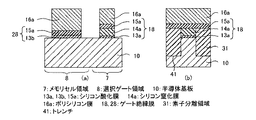
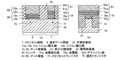
5、71、73、76 メモリセルトランジスタ
6、72、74、75 選択トランジスタ
7 メモリセル領域
8 選択ゲート領域
10 半導体基板
11 素子領域
13 トンネル絶縁層
13a、13b、15a シリコン酸化膜
14 電荷蓄積絶縁膜
14a シリコン窒化膜
15 ブロッキング絶縁膜
16a、53a ポリシリコン膜
17a シリサイド膜
18、28 ゲート絶縁膜
19、29、61、62、63、64、65、66 ゲート電極
21 拡散領域
31 素子分離領域
33 層間絶縁膜
35a、52a 金属膜
41 トレンチ
51a 金属窒化膜
L1、L2 幅
Claims (4)
- 表面に、互いに離間して設けられたソースまたはドレインとなる拡散領域を有する半導体基板と、
前記拡散領域の間の前記半導体基板の表面に、電荷蓄積絶縁膜を有する第1の絶縁膜が配設され、前記第1の絶縁膜の上に接して、不純物がドープされたシリコン及び金属系導電性材料のグループから選択される少なくとも1つの材料が配置された第1のゲート電極を備えたメモリセルトランジスタと、
前記拡散領域の間の前記半導体基板の表面に、第2の絶縁膜が配設され、前記第2の絶縁膜の上に接して、前記不純物がドープされたシリコン及び前記金属系導電性材料のグループから選択される少なくとも1つの材料が配置された第2のゲート電極を備えた選択トランジスタとを具備し、
前記第1のゲート電極に配置され前記第1の絶縁膜の上に接する材料と、前記第2のゲート電極に配置され前記第2の絶縁膜の上に接する材料とは異なり、
前記第1のゲート電極は、前記第1の絶縁膜の上に接して設けられた金属窒化物を含む多層構造であることを特徴とするチャージトラップ型の不揮発性半導体記憶装置。 - 表面に、互いに離間して設けられたソースまたはドレインとなる拡散領域を有する半導体基板と、
前記拡散領域の間の前記半導体基板の表面に、電荷蓄積絶縁膜を有する第1の絶縁膜が配設され、前記第1の絶縁膜の上に接して、不純物がドープされたシリコン及び金属系導電性材料のグループから選択される少なくとも1つの材料が配置された第1のゲート電極を備えたメモリセルトランジスタと、
前記拡散領域の間の前記半導体基板の表面に、第2の絶縁膜が配設され、前記第2の絶縁膜の上に接して、前記不純物がドープされたシリコン及び前記金属系導電性材料のグループから選択される少なくとも1つの材料が配置された第2のゲート電極を備えた選択トランジスタとを具備し、
前記第1のゲート電極に配置され前記第1の絶縁膜の上に接する材料と、前記第2のゲート電極に配置され前記第2の絶縁膜の上に接する材料とは異なり、
前記第1のゲート電極に配置され、前記第1の絶縁膜の上に接する材料は、不純物がドープされたシリコンであり、
前記第2のゲート電極に配置され、前記第2の絶縁膜の上に接する材料は、金属窒化物であることを特徴とするチャージトラップ型の不揮発性半導体記憶装置。 - 前記第2のゲート電極に配置され、前記第2の絶縁膜の上に接する材料は、前記金属単体又は前記金属化合物であることを特徴とする請求項1に記載のチャージトラップ型の不揮発性半導体記憶装置。
- 表面に、互いに離間して設けられたソースまたはドレインとなる拡散領域を有する半導体基板と、
前記拡散領域の間の前記半導体基板の表面に、電荷蓄積絶縁膜を有する第1の絶縁膜が配設され、前記第1の絶縁膜の上に接して、第1の幅を有するシリサイドが配置された第1のゲート電極を備えたメモリセルトランジスタと、
前記拡散領域の間の前記半導体基板の表面に、第2の絶縁膜が配設され、前記第2の絶縁膜の上に接して、順に、第1の幅より大きい第2の幅を有する不純物がドープされたシリコン及び前記シリサイドが配置された第2のゲート電極を備えた選択トランジスタと、
を具備していることを特徴とするチャージトラップ型の不揮発性半導体記憶装置。
Priority Applications (4)
| Application Number | Priority Date | Filing Date | Title |
|---|---|---|---|
| JP2008294786A JP5558695B2 (ja) | 2008-11-18 | 2008-11-18 | 不揮発性半導体記憶装置 |
| US12/618,119 US8134203B2 (en) | 2008-11-18 | 2009-11-13 | Nonvolatile semiconductor memory device |
| US13/364,602 US8575684B2 (en) | 2008-11-18 | 2012-02-02 | Nonvolatile semiconductor memory device |
| US13/364,588 US8614477B2 (en) | 2008-11-18 | 2012-02-02 | Nonvolatile semiconductor memory device |
Applications Claiming Priority (1)
| Application Number | Priority Date | Filing Date | Title |
|---|---|---|---|
| JP2008294786A JP5558695B2 (ja) | 2008-11-18 | 2008-11-18 | 不揮発性半導体記憶装置 |
Publications (3)
| Publication Number | Publication Date |
|---|---|
| JP2010123684A JP2010123684A (ja) | 2010-06-03 |
| JP2010123684A5 JP2010123684A5 (ja) | 2012-01-12 |
| JP5558695B2 true JP5558695B2 (ja) | 2014-07-23 |
Family
ID=42171295
Family Applications (1)
| Application Number | Title | Priority Date | Filing Date |
|---|---|---|---|
| JP2008294786A Active JP5558695B2 (ja) | 2008-11-18 | 2008-11-18 | 不揮発性半導体記憶装置 |
Country Status (2)
| Country | Link |
|---|---|
| US (3) | US8134203B2 (ja) |
| JP (1) | JP5558695B2 (ja) |
Families Citing this family (10)
| Publication number | Priority date | Publication date | Assignee | Title |
|---|---|---|---|---|
| KR101137929B1 (ko) * | 2010-05-31 | 2012-05-09 | 에스케이하이닉스 주식회사 | 비휘발성 메모리 장치 및 그 제조 방법 |
| JP5549411B2 (ja) * | 2010-06-18 | 2014-07-16 | 富士通セミコンダクター株式会社 | 半導体素子の製造方法、半導体メモリの製造方法、及び半導体素子 |
| JP5702227B2 (ja) * | 2011-05-27 | 2015-04-15 | 東京エレクトロン株式会社 | 選択トランジスタ、選択トランジスタの作成方法、メモリ装置及びメモリ装置の製造方法 |
| KR20130004784A (ko) * | 2011-07-04 | 2013-01-14 | 삼성전자주식회사 | 저항 변화 체를 갖는 비-휘발성 메모리 소자 및 그 제조방법 |
| JP6800015B2 (ja) | 2014-01-21 | 2020-12-16 | アプライド マテリアルズ インコーポレイテッドApplied Materials,Incorporated | 3dフラッシュメモリ応用のための誘電体金属スタック |
| JP6250506B2 (ja) | 2014-09-16 | 2017-12-20 | 東芝メモリ株式会社 | 集積回路装置及びその製造方法 |
| US9793289B2 (en) | 2015-06-08 | 2017-10-17 | Toshiba Memory Corporation | Non-volatile memory device |
| JP6696865B2 (ja) * | 2016-08-31 | 2020-05-20 | ルネサスエレクトロニクス株式会社 | 半導体装置およびその製造方法 |
| CN111384060B (zh) * | 2018-12-27 | 2023-11-03 | 爱思开海力士有限公司 | 非易失性存储器件及其制造方法 |
| KR20200126686A (ko) * | 2019-04-30 | 2020-11-09 | 에스케이하이닉스 주식회사 | 반도체 장치의 제조 방법 |
Family Cites Families (18)
| Publication number | Priority date | Publication date | Assignee | Title |
|---|---|---|---|---|
| JPS55156371A (en) * | 1979-05-24 | 1980-12-05 | Toshiba Corp | Non-volatile semiconductor memory device |
| US5838041A (en) * | 1995-10-02 | 1998-11-17 | Kabushiki Kaisha Toshiba | Nonvolatile semiconductor memory device having memory cell transistor provided with offset region acting as a charge carrier injecting region |
| JP2000286349A (ja) | 1999-03-31 | 2000-10-13 | Sony Corp | 半導体装置およびその製造方法 |
| JP4346228B2 (ja) * | 2000-09-21 | 2009-10-21 | 株式会社東芝 | 不揮発性半導体記憶装置及びその製造方法 |
| US6512263B1 (en) * | 2000-09-22 | 2003-01-28 | Sandisk Corporation | Non-volatile memory cell array having discontinuous source and drain diffusions contacted by continuous bit line conductors and methods of forming |
| JP3947041B2 (ja) * | 2001-05-28 | 2007-07-18 | 株式会社東芝 | 半導体装置及びその製造方法 |
| US6897522B2 (en) * | 2001-10-31 | 2005-05-24 | Sandisk Corporation | Multi-state non-volatile integrated circuit memory systems that employ dielectric storage elements |
| US6925007B2 (en) * | 2001-10-31 | 2005-08-02 | Sandisk Corporation | Multi-state non-volatile integrated circuit memory systems that employ dielectric storage elements |
| JP2004039866A (ja) | 2002-07-03 | 2004-02-05 | Toshiba Corp | 半導体装置及びその製造方法 |
| JP2005044844A (ja) * | 2003-07-23 | 2005-02-17 | Toshiba Corp | 不揮発性半導体記憶装置及びその製造方法 |
| JP4041076B2 (ja) * | 2004-02-27 | 2008-01-30 | 株式会社東芝 | データ記憶システム |
| US7829938B2 (en) * | 2005-07-14 | 2010-11-09 | Micron Technology, Inc. | High density NAND non-volatile memory device |
| TWI260769B (en) * | 2005-08-23 | 2006-08-21 | Ememory Technology Inc | Non-volatile memory and operating method thereof |
| JP4965878B2 (ja) * | 2006-03-24 | 2012-07-04 | 株式会社東芝 | 不揮発性半導体メモリ装置 |
| JP5128172B2 (ja) * | 2006-04-28 | 2013-01-23 | 株式会社半導体エネルギー研究所 | 半導体装置の作製方法 |
| JP2008159614A (ja) | 2006-12-20 | 2008-07-10 | Toshiba Corp | 不揮発性半導体メモリ |
| US7846817B2 (en) * | 2007-03-26 | 2010-12-07 | Semiconductor Energy Laboratory Co., Ltd. | Method for manufacturing semiconductor device |
| US8089114B2 (en) * | 2007-11-08 | 2012-01-03 | Samsung Electronics Co., Ltd. | Non-volatile memory devices including blocking and interface patterns between charge storage patterns and control electrodes and related methods |
-
2008
- 2008-11-18 JP JP2008294786A patent/JP5558695B2/ja active Active
-
2009
- 2009-11-13 US US12/618,119 patent/US8134203B2/en active Active
-
2012
- 2012-02-02 US US13/364,588 patent/US8614477B2/en active Active
- 2012-02-02 US US13/364,602 patent/US8575684B2/en active Active
Also Published As
| Publication number | Publication date |
|---|---|
| US8575684B2 (en) | 2013-11-05 |
| US20100123184A1 (en) | 2010-05-20 |
| US8614477B2 (en) | 2013-12-24 |
| US8134203B2 (en) | 2012-03-13 |
| US20120146128A1 (en) | 2012-06-14 |
| US20120139031A1 (en) | 2012-06-07 |
| JP2010123684A (ja) | 2010-06-03 |
Similar Documents
| Publication | Publication Date | Title |
|---|---|---|
| JP5558695B2 (ja) | 不揮発性半導体記憶装置 | |
| US9768185B2 (en) | Non-volatile semiconductor memory device and manufacturing method thereof | |
| JP6026913B2 (ja) | 半導体装置の製造方法 | |
| JP5498011B2 (ja) | 不揮発性半導体記憶装置 | |
| US9349743B2 (en) | Method of manufacturing semiconductor device | |
| JP5221065B2 (ja) | 不揮発性半導体メモリ装置 | |
| JP5210675B2 (ja) | 不揮発性半導体記憶装置及びその製造方法 | |
| US9673208B2 (en) | Method of forming memory array and logic devices | |
| EP2846348A1 (en) | Semiconductor device and method of manufacturing the same | |
| JP2009212218A (ja) | 半導体記憶装置及びその製造方法 | |
| CN106024795B (zh) | 半导体器件及其制造方法 | |
| JP2013045837A (ja) | 不揮発性半導体記憶装置およびその製造方法 | |
| JP2022532474A (ja) | 3次元水平nor型メモリアレイの製造方法 | |
| WO2016088196A1 (ja) | 半導体装置の製造方法および半導体装置 | |
| JP2011029576A (ja) | 不揮発性半導体記憶装置及びその製造方法 | |
| US7986001B2 (en) | Semiconductor memory device and method of manufacturing the same | |
| US20160079265A1 (en) | Nonvolatile semiconductor memory device and method of manufacturing the same | |
| JP2008135715A (ja) | 不揮発性メモリ素子及びその製造方法 | |
| JP5319092B2 (ja) | 半導体装置およびその製造方法 | |
| JP5937172B2 (ja) | 半導体装置および半導体装置の製造方法 | |
| JP2010135561A (ja) | 不揮発性半導体記憶装置 | |
| US7166512B2 (en) | Method of fabricating non-volatile memory | |
| JP4599421B2 (ja) | 半導体装置及びその製造方法 | |
| JP2010182713A (ja) | 不揮発性半導体記憶装置及びその製造方法 | |
| JP5297556B2 (ja) | 不揮発性半導体記憶装置 |
Legal Events
| Date | Code | Title | Description |
|---|---|---|---|
| A521 | Request for written amendment filed |
Free format text: JAPANESE INTERMEDIATE CODE: A523 Effective date: 20111117 |
|
| A621 | Written request for application examination |
Free format text: JAPANESE INTERMEDIATE CODE: A621 Effective date: 20111117 |
|
| RD02 | Notification of acceptance of power of attorney |
Free format text: JAPANESE INTERMEDIATE CODE: A7422 Effective date: 20111125 |
|
| RD04 | Notification of resignation of power of attorney |
Free format text: JAPANESE INTERMEDIATE CODE: A7424 Effective date: 20111205 |
|
| A977 | Report on retrieval |
Free format text: JAPANESE INTERMEDIATE CODE: A971007 Effective date: 20130731 |
|
| A131 | Notification of reasons for refusal |
Free format text: JAPANESE INTERMEDIATE CODE: A131 Effective date: 20130802 |
|
| A521 | Request for written amendment filed |
Free format text: JAPANESE INTERMEDIATE CODE: A523 Effective date: 20130930 |
|
| A521 | Request for written amendment filed |
Free format text: JAPANESE INTERMEDIATE CODE: A523 Effective date: 20131001 |
|
| A131 | Notification of reasons for refusal |
Free format text: JAPANESE INTERMEDIATE CODE: A131 Effective date: 20140110 |
|
| A521 | Request for written amendment filed |
Free format text: JAPANESE INTERMEDIATE CODE: A523 Effective date: 20140310 |
|
| TRDD | Decision of grant or rejection written | ||
| A01 | Written decision to grant a patent or to grant a registration (utility model) |
Free format text: JAPANESE INTERMEDIATE CODE: A01 Effective date: 20140509 |
|
| A61 | First payment of annual fees (during grant procedure) |
Free format text: JAPANESE INTERMEDIATE CODE: A61 Effective date: 20140605 |
|
| R151 | Written notification of patent or utility model registration |
Ref document number: 5558695 Country of ref document: JP Free format text: JAPANESE INTERMEDIATE CODE: R151 |
|
| S111 | Request for change of ownership or part of ownership |
Free format text: JAPANESE INTERMEDIATE CODE: R313111 |
|
| R350 | Written notification of registration of transfer |
Free format text: JAPANESE INTERMEDIATE CODE: R350 |
|
| S111 | Request for change of ownership or part of ownership |
Free format text: JAPANESE INTERMEDIATE CODE: R313111 |
|
| R350 | Written notification of registration of transfer |
Free format text: JAPANESE INTERMEDIATE CODE: R350 |