JP5538672B2 - 半導体装置及びその製造方法並びにデータ処理システム - Google Patents
半導体装置及びその製造方法並びにデータ処理システム Download PDFInfo
- Publication number
- JP5538672B2 JP5538672B2 JP2007275691A JP2007275691A JP5538672B2 JP 5538672 B2 JP5538672 B2 JP 5538672B2 JP 2007275691 A JP2007275691 A JP 2007275691A JP 2007275691 A JP2007275691 A JP 2007275691A JP 5538672 B2 JP5538672 B2 JP 5538672B2
- Authority
- JP
- Japan
- Prior art keywords
- region
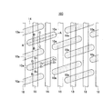
- gate trench
- semiconductor device
- gate
- element isolation
- Prior art date
- Legal status (The legal status is an assumption and is not a legal conclusion. Google has not performed a legal analysis and makes no representation as to the accuracy of the status listed.)
- Expired - Fee Related
Links
Images


Classifications
-
- H—ELECTRICITY
- H10—SEMICONDUCTOR DEVICES; ELECTRIC SOLID-STATE DEVICES NOT OTHERWISE PROVIDED FOR
- H10D—INORGANIC ELECTRIC SEMICONDUCTOR DEVICES
- H10D64/00—Electrodes of devices having potential barriers
- H10D64/01—Manufacture or treatment
- H10D64/025—Manufacture or treatment forming recessed gates, e.g. by using local oxidation
- H10D64/027—Manufacture or treatment forming recessed gates, e.g. by using local oxidation by etching at gate locations
-
- H—ELECTRICITY
- H10—SEMICONDUCTOR DEVICES; ELECTRIC SOLID-STATE DEVICES NOT OTHERWISE PROVIDED FOR
- H10B—ELECTRONIC MEMORY DEVICES
- H10B12/00—Dynamic random access memory [DRAM] devices
- H10B12/01—Manufacture or treatment
- H10B12/02—Manufacture or treatment for one transistor one-capacitor [1T-1C] memory cells
- H10B12/05—Making the transistor
- H10B12/053—Making the transistor the transistor being at least partially in a trench in the substrate
-
- H—ELECTRICITY
- H10—SEMICONDUCTOR DEVICES; ELECTRIC SOLID-STATE DEVICES NOT OTHERWISE PROVIDED FOR
- H10D—INORGANIC ELECTRIC SEMICONDUCTOR DEVICES
- H10D64/00—Electrodes of devices having potential barriers
- H10D64/20—Electrodes characterised by their shapes, relative sizes or dispositions
- H10D64/27—Electrodes not carrying the current to be rectified, amplified, oscillated or switched, e.g. gates
- H10D64/311—Gate electrodes for field-effect devices
- H10D64/411—Gate electrodes for field-effect devices for FETs
- H10D64/511—Gate electrodes for field-effect devices for FETs for IGFETs
- H10D64/512—Disposition of the gate electrodes, e.g. buried gates
- H10D64/513—Disposition of the gate electrodes, e.g. buried gates within recesses in the substrate, e.g. trench gates, groove gates or buried gates
-
- H—ELECTRICITY
- H10—SEMICONDUCTOR DEVICES; ELECTRIC SOLID-STATE DEVICES NOT OTHERWISE PROVIDED FOR
- H10D—INORGANIC ELECTRIC SEMICONDUCTOR DEVICES
- H10D64/00—Electrodes of devices having potential barriers
- H10D64/60—Electrodes characterised by their materials
- H10D64/66—Electrodes having a conductor capacitively coupled to a semiconductor by an insulator, e.g. MIS electrodes
- H10D64/661—Electrodes having a conductor capacitively coupled to a semiconductor by an insulator, e.g. MIS electrodes the conductor comprising a layer of silicon contacting the insulator, e.g. polysilicon having vertical doping variation
- H10D64/662—Electrodes having a conductor capacitively coupled to a semiconductor by an insulator, e.g. MIS electrodes the conductor comprising a layer of silicon contacting the insulator, e.g. polysilicon having vertical doping variation the conductor further comprising additional layers, e.g. multiple silicon layers having different crystal structures
- H10D64/663—Electrodes having a conductor capacitively coupled to a semiconductor by an insulator, e.g. MIS electrodes the conductor comprising a layer of silicon contacting the insulator, e.g. polysilicon having vertical doping variation the conductor further comprising additional layers, e.g. multiple silicon layers having different crystal structures the additional layers comprising a silicide layer contacting the layer of silicon, e.g. polycide gates
Landscapes
- Engineering & Computer Science (AREA)
- Manufacturing & Machinery (AREA)
- Semiconductor Memories (AREA)
- Insulated Gate Type Field-Effect Transistor (AREA)
Priority Applications (2)
| Application Number | Priority Date | Filing Date | Title |
|---|---|---|---|
| JP2007275691A JP5538672B2 (ja) | 2007-10-23 | 2007-10-23 | 半導体装置及びその製造方法並びにデータ処理システム |
| US12/255,817 US7923773B2 (en) | 2007-10-23 | 2008-10-22 | Semiconductor device, manufacturing method thereof, and data processing system |
Applications Claiming Priority (1)
| Application Number | Priority Date | Filing Date | Title |
|---|---|---|---|
| JP2007275691A JP5538672B2 (ja) | 2007-10-23 | 2007-10-23 | 半導体装置及びその製造方法並びにデータ処理システム |
Related Child Applications (1)
| Application Number | Title | Priority Date | Filing Date |
|---|---|---|---|
| JP2014093411A Division JP2014160858A (ja) | 2014-04-30 | 2014-04-30 | 半導体装置 |
Publications (3)
| Publication Number | Publication Date |
|---|---|
| JP2009105227A JP2009105227A (ja) | 2009-05-14 |
| JP2009105227A5 JP2009105227A5 (enExample) | 2011-05-26 |
| JP5538672B2 true JP5538672B2 (ja) | 2014-07-02 |
Family
ID=40562602
Family Applications (1)
| Application Number | Title | Priority Date | Filing Date |
|---|---|---|---|
| JP2007275691A Expired - Fee Related JP5538672B2 (ja) | 2007-10-23 | 2007-10-23 | 半導体装置及びその製造方法並びにデータ処理システム |
Country Status (2)
| Country | Link |
|---|---|
| US (1) | US7923773B2 (enExample) |
| JP (1) | JP5538672B2 (enExample) |
Families Citing this family (8)
| Publication number | Priority date | Publication date | Assignee | Title |
|---|---|---|---|---|
| JP2010050133A (ja) * | 2008-08-19 | 2010-03-04 | Elpida Memory Inc | 半導体装置及び半導体装置の製造方法 |
| US8647935B2 (en) * | 2010-12-17 | 2014-02-11 | International Business Machines Corporation | Buried oxidation for enhanced mobility |
| KR20130055981A (ko) * | 2011-11-21 | 2013-05-29 | 에스케이하이닉스 주식회사 | 반도체 소자의 제조 방법 |
| JP2014022388A (ja) * | 2012-07-12 | 2014-02-03 | Ps4 Luxco S A R L | 半導体装置及びその製造方法 |
| US10084040B2 (en) * | 2015-12-30 | 2018-09-25 | Taiwan Semiconductor Manufacturing Co., Ltd. | Seamless gap fill |
| US20200211840A1 (en) * | 2017-07-19 | 2020-07-02 | Globalwafers Japan Co., Ltd. | Method for producing three-dimensional structure, method for producing vertical transistor, vertical transistor wafer, and vertical transistor substrate |
| US20230197809A1 (en) * | 2021-12-17 | 2023-06-22 | Nanya Technology Corporation | Semiconductor structure having a fin structure |
| TWI817374B (zh) * | 2021-12-17 | 2023-10-01 | 南亞科技股份有限公司 | 具有鰭式結構的半導體結構及其製備方法 |
Family Cites Families (11)
| Publication number | Priority date | Publication date | Assignee | Title |
|---|---|---|---|---|
| JPH06112480A (ja) * | 1992-09-25 | 1994-04-22 | Kawasaki Steel Corp | 半導体装置並びにその製造方法 |
| JPH08274277A (ja) | 1995-03-31 | 1996-10-18 | Toyota Central Res & Dev Lab Inc | 半導体記憶装置およびその製造方法 |
| KR100539276B1 (ko) * | 2003-04-02 | 2005-12-27 | 삼성전자주식회사 | 게이트 라인을 포함하는 반도체 장치 및 이의 제조 방법 |
| US6844591B1 (en) * | 2003-09-17 | 2005-01-18 | Micron Technology, Inc. | Method of forming DRAM access transistors |
| US7189617B2 (en) * | 2005-04-14 | 2007-03-13 | Infineon Technologies Ag | Manufacturing method for a recessed channel array transistor and corresponding recessed channel array transistor |
| JP2007158269A (ja) * | 2005-12-08 | 2007-06-21 | Elpida Memory Inc | 半導体装置及びその製造方法 |
| JP2007194333A (ja) * | 2006-01-18 | 2007-08-02 | Elpida Memory Inc | 半導体装置の製造方法 |
| US7795096B2 (en) * | 2006-12-29 | 2010-09-14 | Qimonda Ag | Method of forming an integrated circuit with two types of transistors |
| JP2008171863A (ja) * | 2007-01-09 | 2008-07-24 | Elpida Memory Inc | トレンチゲートの形成方法 |
| JP2008186979A (ja) * | 2007-01-30 | 2008-08-14 | Elpida Memory Inc | 半導体装置およびその製造方法 |
| JP2009170857A (ja) * | 2007-09-28 | 2009-07-30 | Elpida Memory Inc | 半導体装置及びその製造方法 |
-
2007
- 2007-10-23 JP JP2007275691A patent/JP5538672B2/ja not_active Expired - Fee Related
-
2008
- 2008-10-22 US US12/255,817 patent/US7923773B2/en not_active Expired - Fee Related
Also Published As
| Publication number | Publication date |
|---|---|
| JP2009105227A (ja) | 2009-05-14 |
| US20090101971A1 (en) | 2009-04-23 |
| US7923773B2 (en) | 2011-04-12 |
Similar Documents
| Publication | Publication Date | Title |
|---|---|---|
| JP5538672B2 (ja) | 半導体装置及びその製造方法並びにデータ処理システム | |
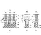
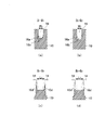
| US8455944B2 (en) | Semiconductor device having a trench-gate transistor | |
| US8299517B2 (en) | Semiconductor device employing transistor having recessed channel region and method of fabricating the same | |
| US8004048B2 (en) | Semiconductor device having a buried gate that can realize a reduction in gate-induced drain leakage (GIDL) and method for manufacturing the same | |
| US20110006365A1 (en) | Semiconductor Device Comprising Transistor Structures and Methods for Forming Same | |
| US20090001458A1 (en) | Semiconductor device with substantial driving current and decreased junction leakage current | |
| US7867856B2 (en) | Method of manufacturing a semiconductor device having fin-field effect transistor | |
| JP5718585B2 (ja) | 半導体装置及びその製造方法、並びにデータ処理システム | |
| JP2000200878A (ja) | 半導体集積回路装置およびその製造方法 | |
| JP2007067391A (ja) | 一対のフィン型チャンネル領域に対応する単一のゲート電極を有する半導体素子の製造方法 | |
| JP2009224520A (ja) | 半導体装置及び半導体装置の製造方法 | |
| KR100625795B1 (ko) | 반도체 소자의 게이트 및 그 형성방법 | |
| US20100044787A1 (en) | Semiconductor device and method of manufacturing the same | |
| US20120001256A1 (en) | Semiconductor device | |
| US20060276001A1 (en) | Method for manufacturing a semiconductor device having a STI structure | |
| US7692251B2 (en) | Transistor for semiconductor device and method of forming the same | |
| JP4470188B2 (ja) | 半導体装置の製造方法 | |
| JP2009009988A (ja) | 半導体装置及びその製造方法 | |
| US7825464B2 (en) | Semiconductor device with recessed active region and gate in a groove | |
| JP2008171863A (ja) | トレンチゲートの形成方法 | |
| JP4600834B2 (ja) | 半導体装置の製造方法 | |
| US20100006930A1 (en) | Semiconductor device, manufacturing method thereof, and data processing system | |
| JP2014160858A (ja) | 半導体装置 | |
| JP2011029509A (ja) | 半導体装置及びその製造方法 | |
| US10608000B1 (en) | Semiconductor device |
Legal Events
| Date | Code | Title | Description |
|---|---|---|---|
| A621 | Written request for application examination |
Free format text: JAPANESE INTERMEDIATE CODE: A621 Effective date: 20100909 |
|
| A521 | Request for written amendment filed |
Free format text: JAPANESE INTERMEDIATE CODE: A523 Effective date: 20110408 |
|
| A711 | Notification of change in applicant |
Free format text: JAPANESE INTERMEDIATE CODE: A711 Effective date: 20130730 |
|
| A521 | Request for written amendment filed |
Free format text: JAPANESE INTERMEDIATE CODE: A523 Effective date: 20130822 |
|
| A131 | Notification of reasons for refusal |
Free format text: JAPANESE INTERMEDIATE CODE: A131 Effective date: 20131126 |
|
| A977 | Report on retrieval |
Free format text: JAPANESE INTERMEDIATE CODE: A971007 Effective date: 20131129 |
|
| A521 | Request for written amendment filed |
Free format text: JAPANESE INTERMEDIATE CODE: A523 Effective date: 20140225 |
|
| TRDD | Decision of grant or rejection written | ||
| A01 | Written decision to grant a patent or to grant a registration (utility model) |
Free format text: JAPANESE INTERMEDIATE CODE: A01 Effective date: 20140401 |
|
| R150 | Certificate of patent or registration of utility model |
Ref document number: 5538672 Country of ref document: JP Free format text: JAPANESE INTERMEDIATE CODE: R150 |
|
| A61 | First payment of annual fees (during grant procedure) |
Free format text: JAPANESE INTERMEDIATE CODE: A61 Effective date: 20140430 |
|
| LAPS | Cancellation because of no payment of annual fees |