JP5421075B2 - 入力回路 - Google Patents
入力回路 Download PDFInfo
- Publication number
- JP5421075B2 JP5421075B2 JP2009258413A JP2009258413A JP5421075B2 JP 5421075 B2 JP5421075 B2 JP 5421075B2 JP 2009258413 A JP2009258413 A JP 2009258413A JP 2009258413 A JP2009258413 A JP 2009258413A JP 5421075 B2 JP5421075 B2 JP 5421075B2
- Authority
- JP
- Japan
- Prior art keywords
- input
- voltage
- node
- power supply
- pmos transistor
- Prior art date
- Legal status (The legal status is an assumption and is not a legal conclusion. Google has not performed a legal analysis and makes no representation as to the accuracy of the status listed.)
- Expired - Fee Related
Links
Images


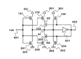

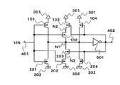


Classifications
-
- H—ELECTRICITY
- H03—ELECTRONIC CIRCUITRY
- H03K—PULSE TECHNIQUE
- H03K19/00—Logic circuits, i.e. having at least two inputs acting on one output; Inverting circuits
- H03K19/003—Modifications for increasing the reliability for protection
- H03K19/00369—Modifications for compensating variations of temperature, supply voltage or other physical parameters
- H03K19/00384—Modifications for compensating variations of temperature, supply voltage or other physical parameters in field effect transistor circuits
-
- H—ELECTRICITY
- H03—ELECTRONIC CIRCUITRY
- H03K—PULSE TECHNIQUE
- H03K3/00—Circuits for generating electric pulses; Monostable, bistable or multistable circuits
- H03K3/01—Details
- H03K3/011—Modifications of generator to compensate for variations in physical values, e.g. voltage, temperature
-
- H—ELECTRICITY
- H03—ELECTRONIC CIRCUITRY
- H03K—PULSE TECHNIQUE
- H03K3/00—Circuits for generating electric pulses; Monostable, bistable or multistable circuits
- H03K3/02—Generators characterised by the type of circuit or by the means used for producing pulses
- H03K3/353—Generators characterised by the type of circuit or by the means used for producing pulses by the use, as active elements, of field-effect transistors with internal or external positive feedback
- H03K3/356—Bistable circuits
- H03K3/3565—Bistables with hysteresis, e.g. Schmitt trigger
-
- H—ELECTRICITY
- H03—ELECTRONIC CIRCUITRY
- H03K—PULSE TECHNIQUE
- H03K5/00—Manipulating of pulses not covered by one of the other main groups of this subclass
- H03K5/15—Arrangements in which pulses are delivered at different times at several outputs, i.e. pulse distributors
- H03K5/151—Arrangements in which pulses are delivered at different times at several outputs, i.e. pulse distributors with two complementary outputs
- H03K5/1515—Arrangements in which pulses are delivered at different times at several outputs, i.e. pulse distributors with two complementary outputs non-overlapping
Landscapes
- Physics & Mathematics (AREA)
- Engineering & Computer Science (AREA)
- Computer Hardware Design (AREA)
- Computing Systems (AREA)
- General Engineering & Computer Science (AREA)
- Mathematical Physics (AREA)
- Nonlinear Science (AREA)
- Logic Circuits (AREA)
- Electronic Switches (AREA)
- Manipulation Of Pulses (AREA)
Priority Applications (5)
| Application Number | Priority Date | Filing Date | Title |
|---|---|---|---|
| JP2009258413A JP5421075B2 (ja) | 2009-11-11 | 2009-11-11 | 入力回路 |
| TW099137779A TW201141065A (en) | 2009-11-11 | 2010-11-03 | Input circuit |
| US12/943,697 US20110109364A1 (en) | 2009-11-11 | 2010-11-10 | Input circuit |
| KR1020100112127A KR20110052520A (ko) | 2009-11-11 | 2010-11-11 | 입력 회로 |
| CN201010553872.2A CN102064694B (zh) | 2009-11-11 | 2010-11-11 | 输入电路 |
Applications Claiming Priority (1)
| Application Number | Priority Date | Filing Date | Title |
|---|---|---|---|
| JP2009258413A JP5421075B2 (ja) | 2009-11-11 | 2009-11-11 | 入力回路 |
Publications (3)
| Publication Number | Publication Date |
|---|---|
| JP2011103607A JP2011103607A (ja) | 2011-05-26 |
| JP2011103607A5 JP2011103607A5 (cg-RX-API-DMAC10.html) | 2012-10-25 |
| JP5421075B2 true JP5421075B2 (ja) | 2014-02-19 |
Family
ID=43973708
Family Applications (1)
| Application Number | Title | Priority Date | Filing Date |
|---|---|---|---|
| JP2009258413A Expired - Fee Related JP5421075B2 (ja) | 2009-11-11 | 2009-11-11 | 入力回路 |
Country Status (5)
| Country | Link |
|---|---|
| US (1) | US20110109364A1 (cg-RX-API-DMAC10.html) |
| JP (1) | JP5421075B2 (cg-RX-API-DMAC10.html) |
| KR (1) | KR20110052520A (cg-RX-API-DMAC10.html) |
| CN (1) | CN102064694B (cg-RX-API-DMAC10.html) |
| TW (1) | TW201141065A (cg-RX-API-DMAC10.html) |
Families Citing this family (6)
| Publication number | Priority date | Publication date | Assignee | Title |
|---|---|---|---|---|
| US9152237B1 (en) * | 2014-06-17 | 2015-10-06 | Realtek Semiconductor Corp. | Power bouncing reduction circuit and method thereof |
| JP7063651B2 (ja) * | 2018-02-19 | 2022-05-09 | エイブリック株式会社 | 信号検出回路及び信号検出方法 |
| JP7361474B2 (ja) * | 2019-01-31 | 2023-10-16 | エイブリック株式会社 | 入力回路 |
| WO2020176793A1 (en) | 2019-02-27 | 2020-09-03 | Nanomosaic Llc | Nanosensors and use thereof |
| JP2022083085A (ja) * | 2020-11-24 | 2022-06-03 | 株式会社東芝 | 半導体集積回路 |
| DE102021111796A1 (de) * | 2021-03-19 | 2022-09-22 | Infineon Technologies Ag | Hochgeschwindigkeitsdigitalsignaltreiber mit niedrigem leistungsverbrauch |
Family Cites Families (14)
| Publication number | Priority date | Publication date | Assignee | Title |
|---|---|---|---|---|
| JPS5877317A (ja) * | 1981-11-02 | 1983-05-10 | Matsushita Electric Ind Co Ltd | シユミツト・トリガ回路 |
| US4539489A (en) * | 1983-06-22 | 1985-09-03 | Motorola, Inc. | CMOS Schmitt trigger circuit |
| US5349246A (en) * | 1992-12-21 | 1994-09-20 | Sgs-Thomson Microelectronics, Inc. | Input buffer with hysteresis characteristics |
| US5386153A (en) * | 1993-09-23 | 1995-01-31 | Cypress Semiconductor Corporation | Buffer with pseudo-ground hysteresis |
| US5459437A (en) * | 1994-05-10 | 1995-10-17 | Integrated Device Technology | Logic gate with controllable hysteresis and high frequency voltage controlled oscillator |
| JPH10229331A (ja) * | 1997-02-14 | 1998-08-25 | Texas Instr Japan Ltd | 入力回路 |
| JPH10290145A (ja) * | 1997-04-14 | 1998-10-27 | Texas Instr Japan Ltd | ヒステリシス回路 |
| KR100266011B1 (ko) * | 1997-10-01 | 2000-09-15 | 김영환 | 히스테리시스입력버퍼 |
| US6433602B1 (en) * | 2000-08-30 | 2002-08-13 | Lattice Semiconductor Corp. | High speed Schmitt Trigger with low supply voltage |
| JP2004096319A (ja) * | 2002-08-30 | 2004-03-25 | Mitsubishi Electric Corp | シュミットトリガ回路 |
| US7183826B2 (en) * | 2004-03-11 | 2007-02-27 | Seiko Epson Corporation | High hysteresis width input circuit |
| CN101385243A (zh) * | 2006-02-16 | 2009-03-11 | Nxp股份有限公司 | 利用迟滞行为将输入信号转换为逻辑输出电压电平 |
| JP4887111B2 (ja) * | 2006-10-12 | 2012-02-29 | オンセミコンダクター・トレーディング・リミテッド | シュミット回路 |
| JP4983562B2 (ja) * | 2007-11-16 | 2012-07-25 | 富士通セミコンダクター株式会社 | シュミット回路 |
-
2009
- 2009-11-11 JP JP2009258413A patent/JP5421075B2/ja not_active Expired - Fee Related
-
2010
- 2010-11-03 TW TW099137779A patent/TW201141065A/zh unknown
- 2010-11-10 US US12/943,697 patent/US20110109364A1/en not_active Abandoned
- 2010-11-11 KR KR1020100112127A patent/KR20110052520A/ko not_active Ceased
- 2010-11-11 CN CN201010553872.2A patent/CN102064694B/zh not_active Expired - Fee Related
Also Published As
| Publication number | Publication date |
|---|---|
| KR20110052520A (ko) | 2011-05-18 |
| CN102064694B (zh) | 2015-06-10 |
| CN102064694A (zh) | 2011-05-18 |
| TW201141065A (en) | 2011-11-16 |
| US20110109364A1 (en) | 2011-05-12 |
| JP2011103607A (ja) | 2011-05-26 |
Similar Documents
| Publication | Publication Date | Title |
|---|---|---|
| KR101505396B1 (ko) | 트랜지스터 스냅백 보호를 탑재한 레벨 시프터 회로 | |
| CN103187963B (zh) | 电平移位电路和使用电平移位电路的半导体器件 | |
| US9584125B2 (en) | Interface circuit | |
| US6930518B2 (en) | Level shifter having low peak current | |
| US8575987B2 (en) | Level shift circuit | |
| US20130222038A1 (en) | Semiconductor integrated circuit | |
| JP4979955B2 (ja) | レベルシフタ回路 | |
| KR20010049227A (ko) | 레벨조정회로 및 이를 포함하는 데이터 출력회로 | |
| JP4768300B2 (ja) | 電圧レベル変換回路及び半導体集積回路装置 | |
| KR20100104124A (ko) | 레벨 쉬프팅이 가능한 로직 회로 | |
| JP2008211707A (ja) | 入力回路 | |
| JP2011103607A (ja) | 入力回路 | |
| KR20140104352A (ko) | 레벨 시프트 회로 | |
| JP3657243B2 (ja) | レベルシフタ、半導体集積回路及び情報処理システム | |
| US8736311B2 (en) | Semiconductor integrated circuit | |
| JP6524829B2 (ja) | レベルシフト回路 | |
| US20090289685A1 (en) | Bias voltage generation for capacitor-coupled level shifter with supply voltage tracking and compensation for input duty-cycle variation | |
| KR100300687B1 (ko) | 반도체집적회로 | |
| KR102845796B1 (ko) | 지연 회로 | |
| US7598791B2 (en) | Semiconductor integrated apparatus using two or more types of power supplies | |
| JP6543485B2 (ja) | 出力バッファ回路 | |
| JP4364752B2 (ja) | 出力回路 | |
| JP2006295322A (ja) | レベルシフタ回路 | |
| JP2006211023A (ja) | 差動増幅回路 | |
| JP2006352204A (ja) | 電位検出回路及びそれを備える半導体集積回路 |
Legal Events
| Date | Code | Title | Description |
|---|---|---|---|
| A521 | Written amendment |
Free format text: JAPANESE INTERMEDIATE CODE: A523 Effective date: 20120911 |
|
| A621 | Written request for application examination |
Free format text: JAPANESE INTERMEDIATE CODE: A621 Effective date: 20120911 |
|
| A977 | Report on retrieval |
Free format text: JAPANESE INTERMEDIATE CODE: A971007 Effective date: 20131011 |
|
| TRDD | Decision of grant or rejection written | ||
| A01 | Written decision to grant a patent or to grant a registration (utility model) |
Free format text: JAPANESE INTERMEDIATE CODE: A01 Effective date: 20131029 |
|
| A61 | First payment of annual fees (during grant procedure) |
Free format text: JAPANESE INTERMEDIATE CODE: A61 Effective date: 20131121 |
|
| R150 | Certificate of patent or registration of utility model |
Ref document number: 5421075 Country of ref document: JP Free format text: JAPANESE INTERMEDIATE CODE: R150 |
|
| S111 | Request for change of ownership or part of ownership |
Free format text: JAPANESE INTERMEDIATE CODE: R313113 |
|
| R350 | Written notification of registration of transfer |
Free format text: JAPANESE INTERMEDIATE CODE: R350 |
|
| R250 | Receipt of annual fees |
Free format text: JAPANESE INTERMEDIATE CODE: R250 |
|
| R250 | Receipt of annual fees |
Free format text: JAPANESE INTERMEDIATE CODE: R250 |
|
| S533 | Written request for registration of change of name |
Free format text: JAPANESE INTERMEDIATE CODE: R313533 |
|
| R350 | Written notification of registration of transfer |
Free format text: JAPANESE INTERMEDIATE CODE: R350 |
|
| R250 | Receipt of annual fees |
Free format text: JAPANESE INTERMEDIATE CODE: R250 |
|
| R250 | Receipt of annual fees |
Free format text: JAPANESE INTERMEDIATE CODE: R250 |
|
| LAPS | Cancellation because of no payment of annual fees |