JP5259122B2 - 表示基板及びこれを有する表示パネル - Google Patents
表示基板及びこれを有する表示パネル Download PDFInfo
- Publication number
- JP5259122B2 JP5259122B2 JP2007137438A JP2007137438A JP5259122B2 JP 5259122 B2 JP5259122 B2 JP 5259122B2 JP 2007137438 A JP2007137438 A JP 2007137438A JP 2007137438 A JP2007137438 A JP 2007137438A JP 5259122 B2 JP5259122 B2 JP 5259122B2
- Authority
- JP
- Japan
- Prior art keywords
- electrode
- substrate
- gate
- wiring
- opening
- Prior art date
- Legal status (The legal status is an assumption and is not a legal conclusion. Google has not performed a legal analysis and makes no representation as to the accuracy of the status listed.)
- Expired - Fee Related
Links
Images


Classifications
-
- G—PHYSICS
- G02—OPTICS
- G02F—OPTICAL DEVICES OR ARRANGEMENTS FOR THE CONTROL OF LIGHT BY MODIFICATION OF THE OPTICAL PROPERTIES OF THE MEDIA OF THE ELEMENTS INVOLVED THEREIN; NON-LINEAR OPTICS; FREQUENCY-CHANGING OF LIGHT; OPTICAL LOGIC ELEMENTS; OPTICAL ANALOGUE/DIGITAL CONVERTERS
- G02F1/00—Devices or arrangements for the control of the intensity, colour, phase, polarisation or direction of light arriving from an independent light source, e.g. switching, gating or modulating; Non-linear optics
- G02F1/01—Devices or arrangements for the control of the intensity, colour, phase, polarisation or direction of light arriving from an independent light source, e.g. switching, gating or modulating; Non-linear optics for the control of the intensity, phase, polarisation or colour
- G02F1/13—Devices or arrangements for the control of the intensity, colour, phase, polarisation or direction of light arriving from an independent light source, e.g. switching, gating or modulating; Non-linear optics for the control of the intensity, phase, polarisation or colour based on liquid crystals, e.g. single liquid crystal display cells
- G02F1/133—Constructional arrangements; Operation of liquid crystal cells; Circuit arrangements
- G02F1/136—Liquid crystal cells structurally associated with a semi-conducting layer or substrate, e.g. cells forming part of an integrated circuit
- G02F1/1362—Active matrix addressed cells
-
- G—PHYSICS
- G02—OPTICS
- G02F—OPTICAL DEVICES OR ARRANGEMENTS FOR THE CONTROL OF LIGHT BY MODIFICATION OF THE OPTICAL PROPERTIES OF THE MEDIA OF THE ELEMENTS INVOLVED THEREIN; NON-LINEAR OPTICS; FREQUENCY-CHANGING OF LIGHT; OPTICAL LOGIC ELEMENTS; OPTICAL ANALOGUE/DIGITAL CONVERTERS
- G02F1/00—Devices or arrangements for the control of the intensity, colour, phase, polarisation or direction of light arriving from an independent light source, e.g. switching, gating or modulating; Non-linear optics
- G02F1/01—Devices or arrangements for the control of the intensity, colour, phase, polarisation or direction of light arriving from an independent light source, e.g. switching, gating or modulating; Non-linear optics for the control of the intensity, phase, polarisation or colour
- G02F1/13—Devices or arrangements for the control of the intensity, colour, phase, polarisation or direction of light arriving from an independent light source, e.g. switching, gating or modulating; Non-linear optics for the control of the intensity, phase, polarisation or colour based on liquid crystals, e.g. single liquid crystal display cells
- G02F1/133—Constructional arrangements; Operation of liquid crystal cells; Circuit arrangements
- G02F1/1333—Constructional arrangements; Manufacturing methods
- G02F1/1343—Electrodes
- G02F1/134309—Electrodes characterised by their geometrical arrangement
-
- G—PHYSICS
- G02—OPTICS
- G02F—OPTICAL DEVICES OR ARRANGEMENTS FOR THE CONTROL OF LIGHT BY MODIFICATION OF THE OPTICAL PROPERTIES OF THE MEDIA OF THE ELEMENTS INVOLVED THEREIN; NON-LINEAR OPTICS; FREQUENCY-CHANGING OF LIGHT; OPTICAL LOGIC ELEMENTS; OPTICAL ANALOGUE/DIGITAL CONVERTERS
- G02F1/00—Devices or arrangements for the control of the intensity, colour, phase, polarisation or direction of light arriving from an independent light source, e.g. switching, gating or modulating; Non-linear optics
- G02F1/01—Devices or arrangements for the control of the intensity, colour, phase, polarisation or direction of light arriving from an independent light source, e.g. switching, gating or modulating; Non-linear optics for the control of the intensity, phase, polarisation or colour
- G02F1/13—Devices or arrangements for the control of the intensity, colour, phase, polarisation or direction of light arriving from an independent light source, e.g. switching, gating or modulating; Non-linear optics for the control of the intensity, phase, polarisation or colour based on liquid crystals, e.g. single liquid crystal display cells
- G02F1/133—Constructional arrangements; Operation of liquid crystal cells; Circuit arrangements
- G02F1/136—Liquid crystal cells structurally associated with a semi-conducting layer or substrate, e.g. cells forming part of an integrated circuit
- G02F1/13606—Liquid crystal cells structurally associated with a semi-conducting layer or substrate, e.g. cells forming part of an integrated circuit having means for reducing parasitic capacitance
-
- G—PHYSICS
- G02—OPTICS
- G02F—OPTICAL DEVICES OR ARRANGEMENTS FOR THE CONTROL OF LIGHT BY MODIFICATION OF THE OPTICAL PROPERTIES OF THE MEDIA OF THE ELEMENTS INVOLVED THEREIN; NON-LINEAR OPTICS; FREQUENCY-CHANGING OF LIGHT; OPTICAL LOGIC ELEMENTS; OPTICAL ANALOGUE/DIGITAL CONVERTERS
- G02F1/00—Devices or arrangements for the control of the intensity, colour, phase, polarisation or direction of light arriving from an independent light source, e.g. switching, gating or modulating; Non-linear optics
- G02F1/01—Devices or arrangements for the control of the intensity, colour, phase, polarisation or direction of light arriving from an independent light source, e.g. switching, gating or modulating; Non-linear optics for the control of the intensity, phase, polarisation or colour
- G02F1/13—Devices or arrangements for the control of the intensity, colour, phase, polarisation or direction of light arriving from an independent light source, e.g. switching, gating or modulating; Non-linear optics for the control of the intensity, phase, polarisation or colour based on liquid crystals, e.g. single liquid crystal display cells
- G02F1/133—Constructional arrangements; Operation of liquid crystal cells; Circuit arrangements
- G02F1/136—Liquid crystal cells structurally associated with a semi-conducting layer or substrate, e.g. cells forming part of an integrated circuit
- G02F1/1362—Active matrix addressed cells
- G02F1/136218—Shield electrodes
Landscapes
- Physics & Mathematics (AREA)
- Nonlinear Science (AREA)
- Mathematical Physics (AREA)
- Chemical & Material Sciences (AREA)
- Crystallography & Structural Chemistry (AREA)
- General Physics & Mathematics (AREA)
- Optics & Photonics (AREA)
- Engineering & Computer Science (AREA)
- Microelectronics & Electronic Packaging (AREA)
- Liquid Crystal (AREA)
- Devices For Indicating Variable Information By Combining Individual Elements (AREA)
Description
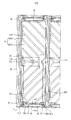
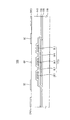
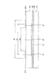
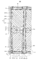
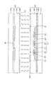
110 ベース基板
120 ゲート絶縁膜
130 パシベーション膜
140 有機絶縁膜
500 表示パネル
620 カラーフィルタ
630 オーバーコーティング膜
640 共通電極
GL ゲート配線
DL データ配線
STL ストレージ配線
TFT 薄膜トランジスタ
PE 画素電極
SPE サブ電極
OP 開口
BM 光遮断パターン
DDP ドメイン分割パターン
SC シールド電極
Claims (22)
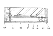
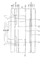
- マトリックス形状に配列される単位画素領域を含むベース基板と、
前記単位画素領域間に延長されたゲート配線と、
前記ゲート配線と交差して前記単位画素領域間に延長されたデータ配線と、
前記単位画素領域内に配置され、前記ゲート配線及びデータ配線と電気的に接続されたスイッチング素子の出力端子と電気的に接続された画素電極と、
前記ゲート配線及びデータ配線の上部に形成され、前記ゲート配線の一部を露出させる開口が形成されたシールド電極と、を含み、
前記シールド電極は、前記画素電極と同じ層に形成されることを特徴とする表示基板。 - 前記シールド電極は、前記画素電極と同じ物質で形成されることを特徴とする請求項1記載の表示基板。
- 前記開口によって形成された前記シールド電極の内側エッジは、前記ゲート配線とオーバーラップされることを特徴とする請求項1記載の表示基板。
- 前記シールド電極は、前記ゲート配線より大きい幅を有して前記ゲート配線をカバーし、前記画素電極と離隔することを特徴とする請求項3記載の表示基板。
- 前記ゲート配線、前記データ配線、及び前記スイッチング素子をカバーする保護絶縁膜を更に含み、
前記画素電極及び前記シールド電極は、前記保護絶縁膜上に形成されることを特徴とする請求項4記載の表示基板。 - 前記保護絶縁膜は、カラーフィルタを含むことを特徴とする請求項5記載の表示基板。
- 前記画素電極は、第1サブ電極及び第2サブ電極を含み、
前記第1サブ電極及び前記第2サブ電極には、前記第1サブ電極及び前記第2サブ電極を複数の領域に分割するドメイン分割パターンが形成されることを特徴とする請求項4記載の表示基板。 - 前記ゲート配線の幅は、前記データ配線と交差する交差部で減少することを特徴とする請求項1記載の表示基板。
- 前記データ配線の幅は、前記ゲート配線と交差する交差部で減少することを特徴とする請求項1記載の表示基板。
- 前記開口の全体幅によって定義される領域は、前記開口の下に配置された前記ゲート配線の幅によって定義される領域内に配置されることを特徴とする請求項1記載の表示基板。
- 下部基板上に配置されたゲート配線と、前記ゲート配線と交差するデータ配線と、前記ゲート配線と前記データ配線とによって定義される単位画素領域内に配置された画素電極と、前記ゲート配線、前記データ配線、及び前記画素電極に電気的に接続されたスイッチング素子と、前記ゲート配線及び前記データ配線の上部に形成され、前記ゲート配線を一部露出させる第1開口が形成されたシールド電極を含む第1基板と、
前記下部基板と対向する上部基板と、前記画素電極に対向して前記上部基板に形成された共通電極を含む第2基板と、
前記第1基板と前記第2基板との間に配置された液晶層と、を含み、
前記シールド電極は、前記画素電極と同じ層に形成されることを特徴とする表示パネル。 - 前記第1基板は、前記ゲート配線、前記データ配線、及び前記スイッチング素子をカバーする保護絶縁膜を更に含み、
前記画素電極及びシールド電極は、前記保護絶縁膜上に形成されることを特徴とする請求項11記載の表示パネル。 - 前記第1開口によって形成された前記シールド電極の内側エッジは前記ゲート配線とオーバーラップされ、
前記シールド電極の外側エッジは、前記画素電極のエッジと前記ゲート配線のエッジとの間に配置されることを特徴とする請求項12記載の表示パネル。 - 前記共通電極には、前記第1開口に対応する第2開口が形成されることを特徴とする請求項12記載の表示パネル。
- 前記第2開口によって形成された前記共通電極の内側エッジは、前記シールド電極の内側エッジと外側エッジとの間に配置されたことを特徴とする請求項14記載の表示パネル。
- 前記第2基板は、
前記ゲート配線、前記データ配線、及び前記スイッチング素子に対応して前記上部基板に形成された光遮断パターンと、
前記単位画素領域に対応するカラーフィルタと、
前記光遮断パターンと前記カラーフィルタとをカバーし、前記共通電極が形成される平坦な面を提供するオーバーコーティング膜と、を更に含むことを特徴とする請求項15記載の表示パネル。 - 前記保護絶縁膜は、カラーフィルタであることを特徴とする請求項12記載の表示パネル。
- 前記画素電極には第1ドメイン分割パターンが形成され、
前記共通電極には前記第1ドメイン分割パターンと交互に配置される第2ドメイン分割パターンが形成されることを特徴とする請求項11記載の表示パネル。 - 前記第1開口の全体幅によって定義される領域は、前記第1開口の下に配置された前記ゲート配線の幅によって定義される領域内に配置されることを特徴とする請求項14記載の表示パネル。
- 前記ゲート配線の全体幅によって定義される領域は、前記ゲート配線の上に配置された前記第2開口の幅によって定義される領域内に配置されることを特徴とする請求項19記載の表示パネル。
- 前記シールド電極は、前記単位画素領域の間に対応して形成されることを特徴とする請求項11記載の表示パネル。
- 前記シールド電極の外側エッジは、前記画素電極のエッジと前記ゲート配線のエッジとの間に配置されることを特徴とする請求項11記載の表示パネル。
Applications Claiming Priority (2)
| Application Number | Priority Date | Filing Date | Title |
|---|---|---|---|
| KR1020060060450A KR101293950B1 (ko) | 2006-06-30 | 2006-06-30 | 표시기판 및 이를 갖는 표시패널 |
| KR10-2006-0060450 | 2006-06-30 |
Publications (2)
| Publication Number | Publication Date |
|---|---|
| JP2008015488A JP2008015488A (ja) | 2008-01-24 |
| JP5259122B2 true JP5259122B2 (ja) | 2013-08-07 |
Family
ID=38876234
Family Applications (1)
| Application Number | Title | Priority Date | Filing Date |
|---|---|---|---|
| JP2007137438A Expired - Fee Related JP5259122B2 (ja) | 2006-06-30 | 2007-05-24 | 表示基板及びこれを有する表示パネル |
Country Status (4)
| Country | Link |
|---|---|
| US (1) | US7973754B2 (ja) |
| JP (1) | JP5259122B2 (ja) |
| KR (1) | KR101293950B1 (ja) |
| CN (1) | CN101097372B (ja) |
Families Citing this family (25)
| Publication number | Priority date | Publication date | Assignee | Title |
|---|---|---|---|---|
| KR101427708B1 (ko) * | 2007-02-01 | 2014-08-11 | 삼성디스플레이 주식회사 | 액정 표시 패널 |
| TW201003269A (en) * | 2008-07-04 | 2010-01-16 | Au Optronics Corp | Liquid crystal display panel and pixel structure thereof |
| KR20100067767A (ko) * | 2008-12-12 | 2010-06-22 | 삼성전자주식회사 | 표시 패널 |
| US8259249B2 (en) * | 2009-10-12 | 2012-09-04 | Samsung Electronics Co., Ltd. | Display substrate, method of manufacturing the display substrate and display device having the display substrate |
| CN102346340B (zh) * | 2010-08-03 | 2014-06-18 | 胜华科技股份有限公司 | 液晶显示面板 |
| CN102645803B (zh) * | 2011-10-17 | 2014-06-18 | 京东方科技集团股份有限公司 | 像素单元,阵列基板、液晶面板、显示装置及其制造方法 |
| KR101830179B1 (ko) * | 2011-11-03 | 2018-02-21 | 삼성디스플레이 주식회사 | 유기 전계 발광 표시 장치 |
| KR20140044453A (ko) | 2012-10-05 | 2014-04-15 | 삼성디스플레이 주식회사 | 표시 기판 및 이를 포함하는 액정 표시 패널 |
| CN103278988A (zh) * | 2013-05-31 | 2013-09-04 | 深圳市华星光电技术有限公司 | 一种基板、显示面板及显示装置 |
| KR102147520B1 (ko) * | 2013-07-29 | 2020-08-25 | 삼성디스플레이 주식회사 | 곡면표시장치 |
| KR20150039404A (ko) * | 2013-10-02 | 2015-04-10 | 삼성디스플레이 주식회사 | 박막 트랜지스터 표시판, 액정 표시 장치 및 박막 트랜지스터 표시판의 제조방법 |
| CN103605241A (zh) * | 2013-11-21 | 2014-02-26 | 深圳市华星光电技术有限公司 | 一种液晶显示面板 |
| KR102140815B1 (ko) | 2013-12-09 | 2020-08-04 | 삼성디스플레이 주식회사 | 액정 표시 장치 |
| KR102134857B1 (ko) * | 2013-12-17 | 2020-07-17 | 삼성디스플레이 주식회사 | 곡면 표시 장치 |
| CN104267546A (zh) * | 2014-09-19 | 2015-01-07 | 京东方科技集团股份有限公司 | 一种阵列基板和显示装置 |
| CN104252071B (zh) * | 2014-09-24 | 2017-10-17 | 深圳市华星光电技术有限公司 | 液晶显示面板及其阵列基板 |
| KR102400081B1 (ko) * | 2015-07-02 | 2022-05-19 | 삼성디스플레이 주식회사 | 표시 장치 |
| KR102430051B1 (ko) * | 2015-11-27 | 2022-08-04 | 엘지디스플레이 주식회사 | 유기 발광 표시 장치 |
| CN105446029A (zh) * | 2016-01-19 | 2016-03-30 | 京东方科技集团股份有限公司 | 一种阵列基板、液晶显示面板及显示装置 |
| KR102542186B1 (ko) * | 2016-04-04 | 2023-06-13 | 삼성디스플레이 주식회사 | 표시 장치 |
| US10416516B2 (en) * | 2017-06-20 | 2019-09-17 | Shenzhen China Star Optoelectronics Technology Co., Ltd | Liquid crystal display panel and liquid crystal display device |
| CN107121864A (zh) * | 2017-07-07 | 2017-09-01 | 深圳市华星光电技术有限公司 | 阵列基板及液晶显示面板 |
| TWI756713B (zh) * | 2019-08-29 | 2022-03-01 | 群創光電股份有限公司 | 顯示裝置 |
| KR102758173B1 (ko) * | 2020-02-21 | 2025-01-24 | 삼성디스플레이 주식회사 | 표시장치 |
| CN112068377A (zh) * | 2020-09-28 | 2020-12-11 | 成都中电熊猫显示科技有限公司 | 阵列基板以及液晶面板 |
Family Cites Families (28)
| Publication number | Priority date | Publication date | Assignee | Title |
|---|---|---|---|---|
| JPS6397919A (ja) * | 1986-10-15 | 1988-04-28 | Seiko Epson Corp | 液晶パネル |
| JP2592600B2 (ja) * | 1987-03-11 | 1997-03-19 | 株式会社フロンテック | 薄膜トランジスタマトリツクスアレイ |
| JPH03209436A (ja) * | 1990-01-12 | 1991-09-12 | Nec Corp | 液晶表示装置 |
| JP3189310B2 (ja) * | 1991-08-28 | 2001-07-16 | セイコーエプソン株式会社 | 液晶装置の製造方法 |
| JPH0561069A (ja) * | 1991-09-04 | 1993-03-12 | Mitsubishi Electric Corp | マトリクス形液晶表示装置 |
| JPH05127195A (ja) * | 1991-11-08 | 1993-05-25 | Toshiba Corp | 液晶表示装置 |
| NL194848C (nl) * | 1992-06-01 | 2003-04-03 | Samsung Electronics Co Ltd | Vloeibaar-kristalindicatorinrichting. |
| EP0592063A3 (en) * | 1992-09-14 | 1994-07-13 | Toshiba Kk | Active matrix liquid crystal display device |
| JPH10325961A (ja) * | 1994-03-17 | 1998-12-08 | Hitachi Ltd | アクティブマトリクス型液晶表示装置 |
| JP3122003B2 (ja) * | 1994-08-24 | 2001-01-09 | シャープ株式会社 | アクティブマトリクス基板 |
| JPH1039336A (ja) * | 1996-07-26 | 1998-02-13 | Toshiba Corp | アクティブマトリクス型液晶表示装置 |
| US6437766B1 (en) * | 1998-03-30 | 2002-08-20 | Sharp Kabushiki Kaisha | LCD driving circuitry with reduced number of control signals |
| JP3766563B2 (ja) * | 1999-05-17 | 2006-04-12 | 株式会社日立製作所 | 液晶表示装置 |
| EP1058310A3 (en) * | 1999-06-02 | 2009-11-18 | Sel Semiconductor Energy Laboratory Co., Ltd. | Semiconductor device and manufacturing method thereof |
| KR100322969B1 (ko) * | 1999-12-22 | 2002-02-01 | 주식회사 현대 디스플레이 테크놀로지 | 인-플레인 스위칭 모드 액정표시장치 및 그의 제조방법 |
| JP3793915B2 (ja) * | 2001-02-28 | 2006-07-05 | 株式会社日立製作所 | 液晶表示装置 |
| JP4728507B2 (ja) * | 2001-06-08 | 2011-07-20 | Nec液晶テクノロジー株式会社 | アクティブマトリクス型液晶表示装置及びその製造方法 |
| JP3879484B2 (ja) * | 2001-10-30 | 2007-02-14 | 株式会社日立製作所 | 液晶表示装置 |
| TW594317B (en) * | 2003-02-27 | 2004-06-21 | Hannstar Display Corp | Pixel structure of in-plane switching liquid crystal display device |
| US7292303B2 (en) * | 2003-07-02 | 2007-11-06 | Samsung Electronics Co., Ltd. | Liquid crystal display and panel therefor including regular and successive regular domain defining members |
| JP2005134889A (ja) * | 2003-10-01 | 2005-05-26 | Samsung Electronics Co Ltd | 薄膜トランジスタ表示板及びこれを含む液晶表示装置 |
| JP2005202125A (ja) * | 2004-01-15 | 2005-07-28 | Seiko Epson Corp | 液晶装置、投射型表示装置および電子機器 |
| CN100451784C (zh) * | 2004-01-29 | 2009-01-14 | 夏普株式会社 | 显示装置 |
| JP2005258004A (ja) * | 2004-03-11 | 2005-09-22 | Toshiba Matsushita Display Technology Co Ltd | 液晶表示素子 |
| KR20060073826A (ko) | 2004-12-24 | 2006-06-29 | 삼성전자주식회사 | 박막 트랜지스터 표시판 |
| KR20060101944A (ko) * | 2005-03-22 | 2006-09-27 | 삼성전자주식회사 | 액정 표시 장치 |
| KR101209051B1 (ko) * | 2005-05-04 | 2012-12-06 | 삼성디스플레이 주식회사 | 박막 트랜지스터 표시판 및 그를 포함하는 액정 표시 장치 |
| KR101294731B1 (ko) * | 2007-06-04 | 2013-08-16 | 삼성디스플레이 주식회사 | 어레이 기판, 이를 갖는 표시패널 및 이의 제조방법 |
-
2006
- 2006-06-30 KR KR1020060060450A patent/KR101293950B1/ko not_active Expired - Fee Related
-
2007
- 2007-04-17 US US11/736,256 patent/US7973754B2/en active Active
- 2007-05-16 CN CN2007101030574A patent/CN101097372B/zh not_active Expired - Fee Related
- 2007-05-24 JP JP2007137438A patent/JP5259122B2/ja not_active Expired - Fee Related
Also Published As
| Publication number | Publication date |
|---|---|
| US7973754B2 (en) | 2011-07-05 |
| JP2008015488A (ja) | 2008-01-24 |
| CN101097372B (zh) | 2010-12-15 |
| KR20080001957A (ko) | 2008-01-04 |
| US20080002123A1 (en) | 2008-01-03 |
| CN101097372A (zh) | 2008-01-02 |
| KR101293950B1 (ko) | 2013-08-07 |
Similar Documents
| Publication | Publication Date | Title |
|---|---|---|
| JP5259122B2 (ja) | 表示基板及びこれを有する表示パネル | |
| US6259200B1 (en) | Active-matrix display apparatus | |
| JP4887531B2 (ja) | 表示装置 | |
| JP4356750B2 (ja) | 液晶表示装置及びその製造方法 | |
| US20040174484A1 (en) | Active matrix type liquid crystal display device and method of manufacturing the same | |
| JP4815584B2 (ja) | 液晶表示装置及びそれに使用される薄膜トランジスタ表示板 | |
| US7880849B2 (en) | Display panel with TFT and gate line disposed between sub-electrodes of pixel electrode | |
| JP2008146017A (ja) | 液晶表示装置 | |
| JP2015049426A (ja) | 液晶表示装置 | |
| KR101112544B1 (ko) | 박막 트랜지스터 표시판 및 그 제조 방법 | |
| JP4826979B2 (ja) | 薄膜トランジスタ表示板及びこれを含む液晶表示装置 | |
| KR20180049371A (ko) | 초고 해상도 액정 표시장치 | |
| US7417691B2 (en) | Display device having a transistor electrode overlapping and disposed within the boundaries of a capacitor electrode | |
| CN100378516C (zh) | 液晶显示器的补偿电容结构 | |
| US20040135939A1 (en) | Liquid crystal display device with light shielding structure and method for forming the same | |
| US20070229745A1 (en) | Display apparatus | |
| WO2015132819A1 (ja) | 液晶表示装置及びその製造方法 | |
| KR101100874B1 (ko) | 박막 트랜지스터 표시판 | |
| KR102098161B1 (ko) | 액정표시장치용 어레이 기판 | |
| JP2006023744A (ja) | 多重ドメイン液晶表示装置及びそれに用いられる表示板 | |
| JP2005182048A (ja) | 多重ドメイン薄膜トランジスタ表示板及びこれを含む液晶表示装置 | |
| JP2006091886A (ja) | カラーフィルタ表示板及びこれを含む液晶表示装置 | |
| KR20090005817A (ko) | 표시기판 및 이를 갖는 표시패널 | |
| KR20080030244A (ko) | 액정 표시 장치 | |
| US7916260B2 (en) | Display substrate, method for manufacturing the same and display apparatus having the same |
Legal Events
| Date | Code | Title | Description |
|---|---|---|---|
| A621 | Written request for application examination |
Free format text: JAPANESE INTERMEDIATE CODE: A621 Effective date: 20100520 |
|
| A521 | Written amendment |
Free format text: JAPANESE INTERMEDIATE CODE: A523 Effective date: 20110421 |
|
| A977 | Report on retrieval |
Free format text: JAPANESE INTERMEDIATE CODE: A971007 Effective date: 20120305 |
|
| A131 | Notification of reasons for refusal |
Free format text: JAPANESE INTERMEDIATE CODE: A131 Effective date: 20120327 |
|
| A601 | Written request for extension of time |
Free format text: JAPANESE INTERMEDIATE CODE: A601 Effective date: 20120626 |
|
| A602 | Written permission of extension of time |
Free format text: JAPANESE INTERMEDIATE CODE: A602 Effective date: 20120629 |
|
| A521 | Written amendment |
Free format text: JAPANESE INTERMEDIATE CODE: A523 Effective date: 20120723 |
|
| A131 | Notification of reasons for refusal |
Free format text: JAPANESE INTERMEDIATE CODE: A131 Effective date: 20121002 |
|
| A711 | Notification of change in applicant |
Free format text: JAPANESE INTERMEDIATE CODE: A712 Effective date: 20121213 |
|
| A521 | Written amendment |
Free format text: JAPANESE INTERMEDIATE CODE: A523 Effective date: 20121228 |
|
| TRDD | Decision of grant or rejection written | ||
| A01 | Written decision to grant a patent or to grant a registration (utility model) |
Free format text: JAPANESE INTERMEDIATE CODE: A01 Effective date: 20130402 |
|
| A61 | First payment of annual fees (during grant procedure) |
Free format text: JAPANESE INTERMEDIATE CODE: A61 Effective date: 20130424 |
|
| FPAY | Renewal fee payment (event date is renewal date of database) |
Free format text: PAYMENT UNTIL: 20160502 Year of fee payment: 3 |
|
| R150 | Certificate of patent or registration of utility model |
Free format text: JAPANESE INTERMEDIATE CODE: R150 Ref document number: 5259122 Country of ref document: JP Free format text: JAPANESE INTERMEDIATE CODE: R150 |
|
| R250 | Receipt of annual fees |
Free format text: JAPANESE INTERMEDIATE CODE: R250 |
|
| R250 | Receipt of annual fees |
Free format text: JAPANESE INTERMEDIATE CODE: R250 |
|
| R250 | Receipt of annual fees |
Free format text: JAPANESE INTERMEDIATE CODE: R250 |
|
| R250 | Receipt of annual fees |
Free format text: JAPANESE INTERMEDIATE CODE: R250 |
|
| R250 | Receipt of annual fees |
Free format text: JAPANESE INTERMEDIATE CODE: R250 |
|
| LAPS | Cancellation because of no payment of annual fees |