JP5259122B2 - Display substrate and display panel having the same - Google Patents
Display substrate and display panel having the same Download PDFInfo
- Publication number
- JP5259122B2 JP5259122B2 JP2007137438A JP2007137438A JP5259122B2 JP 5259122 B2 JP5259122 B2 JP 5259122B2 JP 2007137438 A JP2007137438 A JP 2007137438A JP 2007137438 A JP2007137438 A JP 2007137438A JP 5259122 B2 JP5259122 B2 JP 5259122B2
- Authority
- JP
- Japan
- Prior art keywords
- electrode
- substrate
- gate
- wiring
- opening
- Prior art date
- Legal status (The legal status is an assumption and is not a legal conclusion. Google has not performed a legal analysis and makes no representation as to the accuracy of the status listed.)
- Expired - Fee Related
Links
Images


Classifications
-
- G—PHYSICS
- G02—OPTICS
- G02F—OPTICAL DEVICES OR ARRANGEMENTS FOR THE CONTROL OF LIGHT BY MODIFICATION OF THE OPTICAL PROPERTIES OF THE MEDIA OF THE ELEMENTS INVOLVED THEREIN; NON-LINEAR OPTICS; FREQUENCY-CHANGING OF LIGHT; OPTICAL LOGIC ELEMENTS; OPTICAL ANALOGUE/DIGITAL CONVERTERS
- G02F1/00—Devices or arrangements for the control of the intensity, colour, phase, polarisation or direction of light arriving from an independent light source, e.g. switching, gating or modulating; Non-linear optics
- G02F1/01—Devices or arrangements for the control of the intensity, colour, phase, polarisation or direction of light arriving from an independent light source, e.g. switching, gating or modulating; Non-linear optics for the control of the intensity, phase, polarisation or colour
- G02F1/13—Devices or arrangements for the control of the intensity, colour, phase, polarisation or direction of light arriving from an independent light source, e.g. switching, gating or modulating; Non-linear optics for the control of the intensity, phase, polarisation or colour based on liquid crystals, e.g. single liquid crystal display cells
- G02F1/133—Constructional arrangements; Operation of liquid crystal cells; Circuit arrangements
- G02F1/136—Liquid crystal cells structurally associated with a semi-conducting layer or substrate, e.g. cells forming part of an integrated circuit
- G02F1/1362—Active matrix addressed cells
-
- G—PHYSICS
- G02—OPTICS
- G02F—OPTICAL DEVICES OR ARRANGEMENTS FOR THE CONTROL OF LIGHT BY MODIFICATION OF THE OPTICAL PROPERTIES OF THE MEDIA OF THE ELEMENTS INVOLVED THEREIN; NON-LINEAR OPTICS; FREQUENCY-CHANGING OF LIGHT; OPTICAL LOGIC ELEMENTS; OPTICAL ANALOGUE/DIGITAL CONVERTERS
- G02F1/00—Devices or arrangements for the control of the intensity, colour, phase, polarisation or direction of light arriving from an independent light source, e.g. switching, gating or modulating; Non-linear optics
- G02F1/01—Devices or arrangements for the control of the intensity, colour, phase, polarisation or direction of light arriving from an independent light source, e.g. switching, gating or modulating; Non-linear optics for the control of the intensity, phase, polarisation or colour
- G02F1/13—Devices or arrangements for the control of the intensity, colour, phase, polarisation or direction of light arriving from an independent light source, e.g. switching, gating or modulating; Non-linear optics for the control of the intensity, phase, polarisation or colour based on liquid crystals, e.g. single liquid crystal display cells
- G02F1/133—Constructional arrangements; Operation of liquid crystal cells; Circuit arrangements
- G02F1/1333—Constructional arrangements; Manufacturing methods
- G02F1/1343—Electrodes
- G02F1/134309—Electrodes characterised by their geometrical arrangement
-
- G—PHYSICS
- G02—OPTICS
- G02F—OPTICAL DEVICES OR ARRANGEMENTS FOR THE CONTROL OF LIGHT BY MODIFICATION OF THE OPTICAL PROPERTIES OF THE MEDIA OF THE ELEMENTS INVOLVED THEREIN; NON-LINEAR OPTICS; FREQUENCY-CHANGING OF LIGHT; OPTICAL LOGIC ELEMENTS; OPTICAL ANALOGUE/DIGITAL CONVERTERS
- G02F1/00—Devices or arrangements for the control of the intensity, colour, phase, polarisation or direction of light arriving from an independent light source, e.g. switching, gating or modulating; Non-linear optics
- G02F1/01—Devices or arrangements for the control of the intensity, colour, phase, polarisation or direction of light arriving from an independent light source, e.g. switching, gating or modulating; Non-linear optics for the control of the intensity, phase, polarisation or colour
- G02F1/13—Devices or arrangements for the control of the intensity, colour, phase, polarisation or direction of light arriving from an independent light source, e.g. switching, gating or modulating; Non-linear optics for the control of the intensity, phase, polarisation or colour based on liquid crystals, e.g. single liquid crystal display cells
- G02F1/133—Constructional arrangements; Operation of liquid crystal cells; Circuit arrangements
- G02F1/136—Liquid crystal cells structurally associated with a semi-conducting layer or substrate, e.g. cells forming part of an integrated circuit
- G02F1/13606—Liquid crystal cells structurally associated with a semi-conducting layer or substrate, e.g. cells forming part of an integrated circuit having means for reducing parasitic capacitance
-
- G—PHYSICS
- G02—OPTICS
- G02F—OPTICAL DEVICES OR ARRANGEMENTS FOR THE CONTROL OF LIGHT BY MODIFICATION OF THE OPTICAL PROPERTIES OF THE MEDIA OF THE ELEMENTS INVOLVED THEREIN; NON-LINEAR OPTICS; FREQUENCY-CHANGING OF LIGHT; OPTICAL LOGIC ELEMENTS; OPTICAL ANALOGUE/DIGITAL CONVERTERS
- G02F1/00—Devices or arrangements for the control of the intensity, colour, phase, polarisation or direction of light arriving from an independent light source, e.g. switching, gating or modulating; Non-linear optics
- G02F1/01—Devices or arrangements for the control of the intensity, colour, phase, polarisation or direction of light arriving from an independent light source, e.g. switching, gating or modulating; Non-linear optics for the control of the intensity, phase, polarisation or colour
- G02F1/13—Devices or arrangements for the control of the intensity, colour, phase, polarisation or direction of light arriving from an independent light source, e.g. switching, gating or modulating; Non-linear optics for the control of the intensity, phase, polarisation or colour based on liquid crystals, e.g. single liquid crystal display cells
- G02F1/133—Constructional arrangements; Operation of liquid crystal cells; Circuit arrangements
- G02F1/136—Liquid crystal cells structurally associated with a semi-conducting layer or substrate, e.g. cells forming part of an integrated circuit
- G02F1/1362—Active matrix addressed cells
- G02F1/136218—Shield electrodes
Landscapes
- Physics & Mathematics (AREA)
- Nonlinear Science (AREA)
- Mathematical Physics (AREA)
- Chemical & Material Sciences (AREA)
- Crystallography & Structural Chemistry (AREA)
- General Physics & Mathematics (AREA)
- Optics & Photonics (AREA)
- Engineering & Computer Science (AREA)
- Microelectronics & Electronic Packaging (AREA)
- Liquid Crystal (AREA)
- Devices For Indicating Variable Information By Combining Individual Elements (AREA)
Description
本発明は、表示基板及びこれを有する表示パネルに関する。より詳細には、ゲート信号遅延を緩和させる表示基板及びこれを有する表示パネルに関する。 The present invention relates to a display substrate and a display panel having the display substrate. More specifically, the present invention relates to a display substrate that reduces gate signal delay and a display panel having the same.
一般に、液晶表示パネルは、薄膜トランジスタと画素電極とを有するアレイ基板、カラーフィルタと共通電極とを有するカラーフィルタ、及びアレイ基板とカラーフィルタ基板との間に介在された液晶層を含む。ここで、アレイ基板は、互いに垂直に交差され、複数の単位画素を定義するゲート配線及びデータ配線を更に含み、薄膜トランジスタ及び画素電極は一般的に単位画素内に形成される。 In general, a liquid crystal display panel includes an array substrate having a thin film transistor and a pixel electrode, a color filter having a color filter and a common electrode, and a liquid crystal layer interposed between the array substrate and the color filter substrate. Here, the array substrate further includes a gate line and a data line that intersect each other vertically and define a plurality of unit pixels, and the thin film transistor and the pixel electrode are generally formed in the unit pixel.
液晶表示パネルに表示される画像の画質は、ゲート配線及びデータ配線に印加される信号の正常な伝達に大きく影響を受ける。 The image quality of an image displayed on the liquid crystal display panel is greatly influenced by normal transmission of signals applied to the gate wiring and the data wiring.
特に、液晶表示パネルの画面が大型化される場合、ゲート信号配線の長さが増加し、時定数が増加して、高解像度になると、薄膜トランジスタの導通時間は相対的に減少する。従って、大型及び高解像度液晶表示パネルであるほど、ゲート信号配線の時定数が充分に小さくなければ、ゲート信号遅延が増加し、ゲートICの出力が不充分になるという問題点がある。液晶表示パネルの画面が大型化され、高解像度の画質が要求されることにより、従来の60Hz駆動で120Hzの信号周波数で画像を表示する駆動方式を使用する場合、ゲート信号遅延がより問題になる。 In particular, when the screen of the liquid crystal display panel is enlarged, the gate signal wiring length is increased, the time constant is increased, and when the resolution is increased, the conduction time of the thin film transistor is relatively decreased. Therefore, the larger and higher resolution liquid crystal display panel has a problem that if the time constant of the gate signal wiring is not sufficiently small, the gate signal delay increases and the output of the gate IC becomes insufficient. Since the screen of the liquid crystal display panel is enlarged and high-resolution image quality is required, the gate signal delay becomes more problematic when using the conventional driving method for displaying an image at a signal frequency of 120 Hz with 60 Hz driving. .
ゲート信号遅延は、ゲート配線の抵抗が大きく、ゲート配線に形成される寄生キャパシタが大きいほど増加する。従って、ゲート信号遅延を減少させるために、ゲート配線の材料に用いられる低抵抗メタルについての研究が続けられており、寄生キャパシタの発生を抑制する設計が行われている。 The gate signal delay increases as the resistance of the gate wiring increases and the parasitic capacitor formed in the gate wiring increases. Therefore, in order to reduce the gate signal delay, research on low-resistance metal used as a material for the gate wiring has been continued, and a design for suppressing the generation of parasitic capacitors has been performed.
一方、最近、液晶表示パネルの側面視野角を向上させるために、画素電極をパターニングして単位画素領域を複数個のドメインに分割するPVAモード及びパターニングされた画素電極を電気的に互いに分離されたサブ電極に分割するSPVAモードの液晶表示パネルが開発されている。特に、SPVAモードにおいて、1つの単位画素領域に形成されたサブ電極が互いに異なるゲート配線に接続された場合、ゲート信号遅延は、正常な画像表示に大きな障害となる。 On the other hand, recently, in order to improve the side viewing angle of the liquid crystal display panel, the pixel electrode is patterned and the unit pixel region is divided into a plurality of domains, and the patterned pixel electrode is electrically separated from each other. An SPVA mode liquid crystal display panel divided into sub-electrodes has been developed. In particular, in the SPVA mode, when the sub-electrodes formed in one unit pixel region are connected to different gate wirings, the gate signal delay becomes a major obstacle to normal image display.
本発明の技術的課題は、このような従来の問題点を解決するためのもので、本発明の目的は、ゲート配線に形成されるキャパシタの寄生容量を減少させて信号遅延を減少させた表示基板を提供することにある。 The technical problem of the present invention is to solve such a conventional problem, and the object of the present invention is to reduce the signal delay by reducing the parasitic capacitance of the capacitor formed on the gate wiring. It is to provide a substrate.
本発明の他の目的は、ゲート配線に形成されるキャパシタの寄生容量を減少させて信号遅延を減少させた表示基板を含む表示パネルを提供することにある。 Another object of the present invention is to provide a display panel including a display substrate in which a parasitic capacitance of a capacitor formed in a gate wiring is reduced to reduce a signal delay.
前記した本発明の目的を実現するために、本発明の一実施例による表示基板は、ベース基板、ゲート配線、データ配線、画素電極、及びシールド電極を含む。ベース基板には、マトリックス形状に配列される複数の単位画素領域が含まれる。ゲート配線は単位画素領域間に延長され、データ配線はゲート配線と交差して単位画素領域間に延長される。画素電極は単位画素領域内に配置され、ゲート配線及びデータ配線と電気的に接続されたスイッチング素子の出力端子と電気的に接続される。シールド電極は、ゲート配線及びデータ配線の上部に形成される。シールド電極にはゲート配線の一部を露出させる開口が形成される。 In order to achieve the object of the present invention, a display substrate according to an embodiment of the present invention includes a base substrate, a gate wiring, a data wiring, a pixel electrode, and a shield electrode. The base substrate includes a plurality of unit pixel regions arranged in a matrix shape. The gate wiring extends between the unit pixel regions, and the data wiring crosses the gate wiring and extends between the unit pixel regions. The pixel electrode is disposed in the unit pixel region and is electrically connected to an output terminal of a switching element electrically connected to the gate wiring and the data wiring. The shield electrode is formed on the gate wiring and the data wiring. An opening for exposing a part of the gate wiring is formed in the shield electrode.
シールド電極は、画素電極と同じ層に同じ物質で形成される。開口により形成されるシールド電極の内側エッジはゲート配線とオーバーラップされる。シールド電極は、ゲート配線より大きい幅を有してゲート配線をカバーし、画素電極と離隔するように配置される。ゲート配線の幅及びデータ配線の幅は、相互に交差する交差部で減少する。画素電極には、ドメイン分割パターンが形成される。 The shield electrode is formed of the same material in the same layer as the pixel electrode. The inner edge of the shield electrode formed by the opening overlaps the gate wiring. The shield electrode has a larger width than the gate wiring, covers the gate wiring, and is arranged to be separated from the pixel electrode. The width of the gate wiring and the width of the data wiring are reduced at the intersections that intersect each other. A domain division pattern is formed on the pixel electrode.
前記した本発明の他の目的を実現するために、本発明の一実施例による表示パネルは、第1基板、第2基板、及び第1基板と第2基板との間に介在される液晶層を含む。第1基板は、下部基板上に配置されたゲート配線と、ゲート配線と交差するデータ配線と、ゲート配線及びデータ配線によって定義される単位画素領域内に配置された画素電極と、ゲート配線及びデータ配線を画素電極にスイッチングさせるスイッチング素子と、シールド電極とを含む。シールド電極は、ゲート配線及びデータ配線の上部に形成され、シールド電極にはゲート配線を一部露出させる第1開口が形成される。第2基板は、下部基板と対向する上部基板と、画素電極に対向して上部基板に形成される共通電極とを含む。 In order to achieve another object of the present invention, a display panel according to an embodiment of the present invention includes a first substrate, a second substrate, and a liquid crystal layer interposed between the first substrate and the second substrate. including. The first substrate includes a gate wiring disposed on the lower substrate, a data wiring intersecting with the gate wiring, a pixel electrode disposed in a unit pixel region defined by the gate wiring and the data wiring, a gate wiring, and a data A switching element for switching the wiring to the pixel electrode and a shield electrode are included. The shield electrode is formed above the gate wiring and the data wiring, and a first opening that exposes part of the gate wiring is formed in the shield electrode. The second substrate includes an upper substrate facing the lower substrate and a common electrode formed on the upper substrate facing the pixel electrode.
一実施例において、第1基板は、ゲート配線、データ配線、及びスイッチング素子をカバーする保護絶縁膜を更に含む。画素電極及びシールド電極は、保護絶縁膜上に形成される。第1開口により形成されるシールド電極の内側エッジはゲート配線とオーバーラップされ、シールド電極の外側エッジは画素電極のエッジとゲート配線のエッジとの間に配置される。共通電極には、第1開口に対応する第2開口が形成される。第2開口により形成される共通電極の内側エッジは、シールド電極の内側エッジと外側エッジとの間に配置される。第2基板は、光遮断パターン、カラーフィルタ、及びオーバーコーティング膜を更に含む。光遮断パターンは、ゲート配線、データ配線、及びスイッチング素子に対応して上部基板に形成される。カラーフィルタは、単位画素領域に対応して形成される。保護膜は、光遮断パターンとカラーフィルタとをカバーし、共通電極は保護膜上に形成される。画素電極には、第1ドメイン分割パターンが形成され、共通電極には第1ドメイン分割パターンと交互に配置される第2ドメイン分割パターンが形成される。 In one embodiment, the first substrate further includes a protective insulating film covering the gate wiring, the data wiring, and the switching element. The pixel electrode and the shield electrode are formed on the protective insulating film. The inner edge of the shield electrode formed by the first opening overlaps with the gate wiring, and the outer edge of the shield electrode is disposed between the edge of the pixel electrode and the edge of the gate wiring. A second opening corresponding to the first opening is formed in the common electrode. The inner edge of the common electrode formed by the second opening is disposed between the inner edge and the outer edge of the shield electrode. The second substrate further includes a light blocking pattern, a color filter, and an overcoating film. The light blocking pattern is formed on the upper substrate corresponding to the gate wiring, the data wiring, and the switching element. The color filter is formed corresponding to the unit pixel region. The protective film covers the light blocking pattern and the color filter, and the common electrode is formed on the protective film. A first domain division pattern is formed on the pixel electrode, and a second domain division pattern alternately arranged with the first domain division pattern is formed on the common electrode.
本発明の表示基板及びこれを有する表示パネルによると、大型及び高解像度を有する表示パネルでゲート遅延を減少させて良質の画像を実現することができる。 According to the display substrate and the display panel having the same of the present invention, a high-quality image can be realized by reducing gate delay in a large-sized and high-resolution display panel.
以下、添付図面を参照して、本発明の好ましい実施例を詳細に説明する。 Hereinafter, preferred embodiments of the present invention will be described in detail with reference to the accompanying drawings.
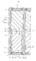
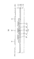
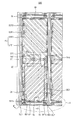
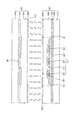
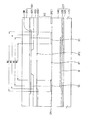
図1乃至図3を参照して、表示基板について以下説明する。図1は、本発明の一実施例による表示基板の平面図である。図2は、図1に図示された表示基板をI−I´線に沿って切断した断面図である。 The display substrate will be described below with reference to FIGS. FIG. 1 is a plan view of a display substrate according to an embodiment of the present invention. FIG. 2 is a cross-sectional view of the display substrate shown in FIG. 1 cut along the line II ′.
図1及び図2を参照すると、表示基板100は、ベース基板110、ゲート配線GL、一対のデータ配線DL1、DL2、画素電極PE、及びシールド電極SCを含む。
1 and 2, the
ベース基板110は、光学的に等方性を有するガラスから形成されてもよい。ベース基板110には、マトリックス形状に配列される複数の単位画素領域が配置される。単位画素領域は、マトリックス形状及びモザイク形状等一定の配列方式によって配置される。
The
ゲート配線GLは、ベース基板110上で単位画素領域間に延長される。データ配線DL1、DL2は、ゲート配線GLと絶縁された状態で、ゲート配線GLが形成されたベース基板110上に配置される。データ配線DL1、DL2は、ゲート配線GLと交差して単位画素領域の間に延長される。ゲート配線GLは、例えば、アルミニウム(Al)、モリブデン(Mo)、タンタル(Ta)、チタニウム(Ti)、タングステン(W)、クロム(Cr)、及び銀(Ag)等で形成されてもよい。
The gate line GL extends between the unit pixel regions on the
ゲート配線GLに印加される制御信号の遅延を減少させるために、ゲート配線GLは抵抗値の小さいメタルで形成されることが好ましく、ゲート配線GLの断面積が大きいことが好ましい。しかし、ゲート配線GLの線幅が非常に大きいと、単位画素領域の開口率が減少し、ゲート配線GLの厚みが非常に厚いと、ゲート配線GLの上部に形成される他の層の形成が容易ではなくなる。本実施例において、ゲート配線GLは、第1の幅を有する。一方、ゲート配線GLとデータ配線DLとの間のオーバーラップされる面積を減少させるために、ゲート配線GLの幅は、データ配線DLと交差する交差部で減少して、データ配線DLの幅はゲート配線GLと交差する交差部で減少することが好ましい。 In order to reduce the delay of the control signal applied to the gate line GL, the gate line GL is preferably formed of a metal having a small resistance value, and the cross-sectional area of the gate line GL is preferably large. However, if the line width of the gate line GL is very large, the aperture ratio of the unit pixel region is reduced. If the gate line GL is very thick, other layers formed on the gate line GL may be formed. It will not be easy. In this embodiment, the gate line GL has a first width. On the other hand, in order to reduce the overlapping area between the gate line GL and the data line DL, the width of the gate line GL decreases at the intersection where the data line DL intersects, and the width of the data line DL becomes It is preferable to decrease at the intersection that intersects with the gate wiring GL.
各単位画素領域には薄膜トランジスタが形成される。薄膜トランジスタは、ゲート配線GL及びデータ配線DL1、DL2と電気的に接続される。各薄膜トランジスタは、各ゲート配線GL又は各データ配線DL1、DL2に沿って配置され、ゲート配線GL及びデータ配線DL1、DL2と電気的に接続され、ゲート配線GLから印加された制御信号によってデータ配線DL1、DL2から印加された画素電圧を出力する。 A thin film transistor is formed in each unit pixel region. The thin film transistor is electrically connected to the gate line GL and the data lines DL1 and DL2. Each thin film transistor is disposed along each gate line GL or each data line DL1, DL2, is electrically connected to the gate line GL and the data lines DL1, DL2, and is connected to the data line DL1 by a control signal applied from the gate line GL. , The pixel voltage applied from DL2 is output.
本実施例において、1つの単位画素領域には1つのゲート配線GLと2つのデータ配線DL1、DL2が対応する。従って、単位画素領域を中心に薄膜トランジスタを説明する。単位画素領域に対応する2つのデータ配線DL1、DL2をそれぞれ第1データ配線DL1及び第2データ配線DL2と定義する。第1データ配線DL1と接続された薄膜トランジスタを第1薄膜トランジスタTFT1、第2データ配線DL2と接続された薄膜トランジスタを第2薄膜トランジスタTFT2とそれぞれ定義する。第1及び第2薄膜トランジスタTFT1、TFT2の層状構造は同じなので、説明の便宜のために図1及び図2に図示された第1薄膜トランジスタTFT1を中心に層状構造を説明する。 In this embodiment, one gate line GL and two data lines DL1 and DL2 correspond to one unit pixel region. Accordingly, the thin film transistor will be described focusing on the unit pixel region. Two data lines DL1 and DL2 corresponding to the unit pixel region are defined as a first data line DL1 and a second data line DL2, respectively. A thin film transistor connected to the first data line DL1 is defined as a first thin film transistor TFT1, and a thin film transistor connected to the second data line DL2 is defined as a second thin film transistor TFT2. Since the layered structures of the first and second thin film transistors TFT1 and TFT2 are the same, the layered structure will be described focusing on the first thin film transistor TFT1 shown in FIGS. 1 and 2 for convenience of explanation.
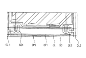
第1薄膜トランジスタTFT1は、図1及び図2に示すように、第1ゲート電極GE1、ゲート絶縁膜120、第1アクティブ層AL1、第1オーミックコンタクト層OL1、第1ソース電極SE1、及び第1ドレイン電極DE1を含む。
As shown in FIGS. 1 and 2, the first thin film transistor TFT1 includes a first gate electrode GE1, a
第1ゲート電極GE1は、ゲート配線GLから突出される。ゲート絶縁膜120は、ゲート配線GLが形成されたベース基板110上に形成される。第1アクティブ層AL1は、例えば、アモルファスシリコンのような半導体からなり、第1ゲート電極GE1に対応するゲート絶縁膜120上に形成される。
The first gate electrode GE1 protrudes from the gate line GL. The
第1ソース電極SE1は、第1データ配線DL1のうち、第1アクティブ層AL1とオーバーラップされる部分で、一例としてU字形状を有する。第1ドレイン電極DE1は、第1ソース電極SE1と同じ層に第1ソース電極SE1から離隔するように形成される。第1ドレイン電極DE1は、一例として、U字形状を有する第1ソース電極SE1の中間に配置される。従って、第1ドレイン電極DE1は第1アクティブ層AL1と一部オーバーラップされ、第1データ配線DL1に沿って延長される。第1オーミックコンタクト層OL1は、例えば、n−typeの不純物がドーピングされたアモルファスシリコンからなり、第1アクティブ層AL1と第1ソース電極SE1との間、及び第1アクティブ層AL1と第1ドレイン電極DE1との間にそれぞれ形成される。 The first source electrode SE1 is a portion of the first data line DL1 that overlaps the first active layer AL1, and has a U-shape as an example. The first drain electrode DE1 is formed in the same layer as the first source electrode SE1 so as to be separated from the first source electrode SE1. For example, the first drain electrode DE1 is disposed in the middle of the first source electrode SE1 having a U shape. Accordingly, the first drain electrode DE1 partially overlaps with the first active layer AL1 and extends along the first data line DL1. The first ohmic contact layer OL1 is made of, for example, amorphous silicon doped with an n-type impurity, and is between the first active layer AL1 and the first source electrode SE1 and between the first active layer AL1 and the first drain electrode. Each is formed between DE1.
表示基板100は、パシベーション層130及び保護絶縁膜140を更に含む。
The
パシベーション層130は、第1薄膜トランジスタTFT1、第2薄膜トランジスタTFT2、第1データ配線DL1、第2データ配線DL2、及びゲート絶縁膜120をカバーする。
The
保護絶縁膜140は、パシベーション層130上に形成され、表面を平坦化させる。本実施例で保護絶縁膜140は、ベース基板110に入射した光の色相をそのまま維持する有機絶縁膜140である。これとは異なる他の実施例において、保護絶縁膜140は、単位画素領域別に互いに異なる色相を有するカラーフィルタであってもよい。ここで、パシベーション層130及び保護絶縁膜140のうち、いずれか1つは省略されてもよい。
The protective
画素電極PEは、有機絶縁膜140上の単位画素領域に形成される。画素電極PEは透明な導電性物質からなり、一例として、酸化スズインジウム(ITO)、酸化亜鉛インジウム(IZO)、アモルファス酸化スズインジウム(a−ITO)等からなる。
The pixel electrode PE is formed in the unit pixel region on the organic insulating
本実施例で、画素電極PEは電気的に互いに分離された第1サブ電極SPE1及び第2サブ電極SPE2を含む。第1サブ電極SPE1及び第2サブ電極SPE2にはドメイン分割パターンDDPが形成される。本実施例でドメイン分割パターンDDPは、第1サブ電極SPE1及び第2サブ電極SPE2の一部がV字形状に除去された開口パターンである。これとは異なる他の実施例において、ドメイン分割パターンDDPは、突起パターンであってもよい。 In this embodiment, the pixel electrode PE includes a first sub-electrode SPE1 and a second sub-electrode SPE2 that are electrically separated from each other. A domain division pattern DDP is formed on the first sub electrode SPE1 and the second sub electrode SPE2. In this embodiment, the domain division pattern DDP is an opening pattern in which a part of the first sub electrode SPE1 and the second sub electrode SPE2 is removed in a V shape. In another embodiment different from this, the domain division pattern DDP may be a protrusion pattern.
第1サブ電極SPE1は、有機絶縁膜140に形成された第1コンタクトホール142を通じて第1薄膜トランジスタTFT1の第1ドレイン電極DE1と電気的に接続され、第2サブ電極SPE2は第2コンタクトホール144を通じて第2薄膜トランジスタTFT2の第2ドレイン電極DE2と電気的に接続される。
The first sub electrode SPE1 is electrically connected to the first drain electrode DE1 of the first thin film transistor TFT1 through the
表示基板100は、ストレージ配線STLを更に含む。ストレージ配線STLはゲート配線GLと同じ層に形成され、ゲート配線GLと平行に単位画素領域を横切るように配置されてもよい。ストレージ配線STLのうち、単位画素領域内に対応する部分はその幅が増加してストレージ電極STEを形成する。
The
図3は、図1に図示された表示基板をII−II´線に沿って切断した断面図である。 FIG. 3 is a cross-sectional view of the display substrate shown in FIG. 1 cut along the line II-II ′.
図1、図2、及び図3を参照すると、シールド電極SCは、画素電極PEと同様に、有機絶縁膜140上に画素電極PEと同じ物質で形成される。シールド電極SCは単位画素領域の間に対応して形成される。従って、シールド電極SCはゲート配線GL及びデータ配線DL1、DL2の上部に形成される。ゲート配線GLに対応するシールド電極SCはゲート配線GLの第1の幅W1より大きい第2の幅W2を有してゲート配線GLを完全にカバーする。シールド電極SCの外側エッジは、画素電極PEのエッジとゲート配線GLのエッジとの間に配置される。
Referring to FIGS. 1, 2, and 3, the shield electrode SC is formed of the same material as the pixel electrode PE on the organic insulating
本実施例でゲート配線GLと画素電極PE及びデータ配線DL1、DL2と画素電極PEは、平面図上でオーバーラップされないが、数乃至数十マイクロスケールに近接して形成される。従って、ゲート絶縁膜120、パシベーション膜130、及び有機絶縁膜140を誘電体としてゲート配線GLと画素電極PEとの間には第1寄生キャパシタが形成され、データ配線DL1、DL2と画素電極PEとの間には第2寄生キャパシタが形成される。
In this embodiment, the gate line GL and the pixel electrode PE, and the data lines DL1 and DL2 and the pixel electrode PE are not overlapped on the plan view, but are formed close to several to several tens of microscales. Accordingly, a first parasitic capacitor is formed between the gate line GL and the pixel electrode PE using the
シールド電極SCは、ゲート配線GL及びデータ配線DL1、DL2の上部に形成されるので、シールド電極SCとゲート配線GLとの間及びシールド電極SCとデータ配線DL1、DL2との間には第3寄生キャパシタが形成される。第3寄生キャパシタが形成される場合、第1寄生キャパシタ及び第2寄生キャパシタのサイズが非常に小さくなる。従って、第1寄生キャパシタ及び第2寄生キャパシタにより画素電極PEに印加される画素電圧が歪曲される程度及びデータ信号が歪曲される程度が減少する。 Since the shield electrode SC is formed on the gate line GL and the data lines DL1 and DL2, a third parasitic line is formed between the shield electrode SC and the gate line GL and between the shield electrode SC and the data lines DL1 and DL2. A capacitor is formed. When the third parasitic capacitor is formed, the size of the first parasitic capacitor and the second parasitic capacitor becomes very small. Accordingly, the degree to which the pixel voltage applied to the pixel electrode PE is distorted by the first parasitic capacitor and the second parasitic capacitor and the degree to which the data signal is distorted are reduced.
一方、ゲート信号遅延を減少させるためには、ゲート配線GLに形成される寄生キャパシタが小さいほど好ましい。従って、第3寄生キャパシタも減少させることが好ましい。 On the other hand, in order to reduce the gate signal delay, it is preferable that the parasitic capacitor formed in the gate wiring GL is smaller. Therefore, it is preferable to reduce the third parasitic capacitor.
本実施例で、ゲート配線GLの上部に形成されたシールド電極SCには、シールド電極SCの一部が除去された開口OPが形成される。開口OPは、ゲート配線GLに沿って長く延長され、ゲート配線GLの第1の幅W1より小さい第3の幅W3を有する。開口OPは、ゲート配線GLに完全にオーバーラップされるように形成される。即ち、開口OPにより形成されたシールド電極SCの内側エッジはゲート配線GLとオーバーラップされる。即ち、開口OPの第3の幅W3(全体幅)はゲート配線GLの第1の幅W1上に直接的に配置される。従って、シールド電極SCに開口OPが形成されても、シールド電極SCの一部はゲート配線GLとオーバーラップされるので、第3寄生キャパシタが形成され、その結果、第1寄生キャパシタ及び第2寄生キャパシタが形成されることを遮断する効果は残る。 In the present embodiment, an opening OP from which a part of the shield electrode SC is removed is formed in the shield electrode SC formed above the gate wiring GL. The opening OP extends long along the gate line GL and has a third width W3 that is smaller than the first width W1 of the gate line GL. The opening OP is formed so as to completely overlap the gate wiring GL. That is, the inner edge of the shield electrode SC formed by the opening OP is overlapped with the gate line GL. That is, the third width W3 (overall width) of the opening OP is directly arranged on the first width W1 of the gate wiring GL. Therefore, even if the opening OP is formed in the shield electrode SC, a part of the shield electrode SC is overlapped with the gate wiring GL, so that a third parasitic capacitor is formed. As a result, the first parasitic capacitor and the second parasitic capacitor are formed. The effect of blocking the formation of the capacitor remains.
シールド電極SCとゲート配線GLのオーバーラップされる面積が大きいほど、シールド電極SCとゲート配線GL間の離隔間隔が小さいほど、及びゲート絶縁膜120、パシベーション膜130及び有機絶縁膜140の誘電率が大きいほど、第3寄生キャパシタが増加する。
The dielectric constants of the
本実施例において、シールド電極SCに形成される開口OPによって第3寄生キャパシタは大幅に減少する。又、ゲート配線GLの線幅を増加させても、シールド電極SCに形成された開口OPによって第3寄生キャパシタは殆ど増加しない。従って、ゲート配線GLの線幅を増加させてゲート配線GLの抵抗を減少させることができ、シールド電極SCに形成された開口OPによって第3寄生キャパシタが減少し、ゲート信号遅延を減少させることができる。 In the present embodiment, the third parasitic capacitor is greatly reduced by the opening OP formed in the shield electrode SC. Further, even if the line width of the gate wiring GL is increased, the third parasitic capacitor hardly increases due to the opening OP formed in the shield electrode SC. Accordingly, the resistance of the gate line GL can be reduced by increasing the line width of the gate line GL, and the third parasitic capacitor can be reduced by the opening OP formed in the shield electrode SC, thereby reducing the gate signal delay. it can.
図4乃至図9を参照して、表示パネルについて以下説明する。図4は、本発明の一実施例による表示パネルの平面図である。 The display panel will be described below with reference to FIGS. FIG. 4 is a plan view of a display panel according to an embodiment of the present invention.
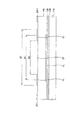
図4を参照すると、表示パネル500は、第1基板501、第2基板601、及び第1基板と第2基板601との間に介在される液晶層LCを含む。第1基板501は、図1乃至図3に図示された表示基板100と実質的に同じである。
Referring to FIG. 4, the
従って、単位画素領域を基準に観察すると、第1基板501は、下部基板510と、下部基板510上に配置されたゲート配線GLと、ゲート配線GLと交差する第1データ配線DL1及び第2データ配線DL2と、ゲート配線GL、第1データ配線DL1及び第2データ配線DL2によって定義される単位画素領域内に配置された画素電極PEと、ゲート配線GL、第1データ配線DL1、及び第2データ配線DL2を画素電極PEにスイッチングさせる第1薄膜トランジスタTFT1及び第2薄膜トランジスタTFT2と、単位画素領域間に形成されたシールド電極SCとを含む。
Accordingly, when observing the unit pixel region as a reference, the
シールド電極SCは、ゲート配線GL、第1データ配線DL1及び第2データ配線DL2の上部に形成され、ゲート配線GLに対応するシールド電極SCには第1開口OP1が形成される。 The shield electrode SC is formed above the gate line GL, the first data line DL1, and the second data line DL2, and the first opening OP1 is formed in the shield electrode SC corresponding to the gate line GL.
下部基板510、画素電極PEに形成される第1ドメイン分割パターンDDP1及びシールド電極SCに形成される第1開口OP1は、図1乃至図3に図示されたベース基板110、ドメイン分割パターンDDP、及び開口OPにそれぞれ対応する。
The first substrate division pattern DDP1 formed in the
図5は、図4に図示された表示パネルの第2基板の平面図である。図6は、図4に図示された表示パネルをIII−III´線に沿って切断した断面図である。図7は、図4に図示された表示パネルをIV−IV´線に沿って切断した断面図である。 FIG. 5 is a plan view of a second substrate of the display panel shown in FIG. 6 is a cross-sectional view of the display panel shown in FIG. 4 cut along the line III-III ′. FIG. 7 is a cross-sectional view of the display panel shown in FIG. 4 cut along the line IV-IV ′.
図5、図6、及び図7を参照すると、第2基板601は、第1基板501の下部基板510と対向する上部基板610、光遮断パターンBM、カラーフィルタ620、オーバーコーティング膜630、及び共通電極640を含む。
Referring to FIGS. 5, 6, and 7, the
光遮断パターンBMは、下部基板510と対向する上部基板610の第1の領域(面)に形成される。光遮断パターンBMは、図4に示すように、単位画素領域間の境界領域、第1薄膜トランジスタTFT1、第2薄膜トランジスタTFT2、ゲート配線GL、第1データ配線DL1、第2データ配線DL2、及びストレージ配線STLをカバーする。光遮断パターンBMは、単位画素領域に対応する形状を有する開口部を定義する。光遮断パターンBMは有機物を含むことが好ましいが、クロム(Cr)のような無機物を含んでもよい。
The light blocking pattern BM is formed in the first region (surface) of the
カラーフィルタ620は開口部に形成され、光遮断パターンBMと一部オーバーラップされる。カラーフィルタ620は、赤色カラーフィルタ、緑色カラーフィルタ、及び青色カラーフィルタのうち、いずれか一つである。赤色カラーフィルタ、緑色カラーフィルタ、及び青色カラーフィルタは、ストライプタイプ及びモザイクタイプ等所定の配列方式によって配列される。
The
本実施例と異なり、パシベーション膜530上に形成された有機絶縁膜540に代替してカラーフィルタ620を第1基板501上に形成する場合、第2基板601上にカラーフィルタは省略されてもよい。
Unlike the present embodiment, when the
オーバーコーティング膜630は、カラーフィルタ620及び光遮断パターンBMをカバーして保護し、第2基板601の表面を平坦化させる。オーバーコーティング膜630は、透明な有機物からなることが好ましい。
The
共通電極640は、オーバーコーティング膜630上に画素電極PEと同じ材質で形成される。共通電極640には、単位画素領域に対応して第2ドメイン分割パターンDDP2、例えば、開口パターンが形成される。第1ドメイン分割パターンDDP1と第2ドメイン分割パターンDDP2とは交互に配置される。その結果、単位画素領域は、複数個のドメインに分割される。ここで、ドメインは液晶の配列方向が不連続的に変わる位置を境界として区分される領域で定義される。
The
ゲート配線GLと共通電極640とがオーバーラップされる場合、ゲート配線GLに第4寄生キャパシタが形成され、第4寄生キャパシタは、ゲート信号遅延を増加させる。本実施例では、ゲート配線GLと共通電極640との間のオーバーラップされる面積を少なくするために、ゲート配線GLに対応する共通電極640の一部が除去され第2開口OP2が形成される。第2開口OP2は、シールド電極SCに形成された第1開口OP1に対応する。
When the gate line GL and the
液晶層LCは、図6に示すように、第1基板501と第2基板601との間に介在される。互いに隣り合うドメインで液晶層LCに含まれる液晶分子は、それぞれ互いに異なる方向に配列される。これによって、1つの単位画素領域から出射される光の視野角が増加する。
The liquid crystal layer LC is interposed between the
図8は、図4に図示された第1領域の拡大図である。図9は、図4に図示されたV−V´線に沿って切断した断面図である。 FIG. 8 is an enlarged view of the first region shown in FIG. FIG. 9 is a cross-sectional view taken along the line VV ′ shown in FIG.
図8及び図9を参照すると、ゲート配線GLは第1の幅W1を有する。ゲート配線GLをカバーするシールド電極SCは、第1の幅W1より大きい第2の幅W2を有し、画素電極PEと離隔される。従って、シールド電極SCの外側エッジは、画素電極PEのエッジとゲート配線GLのエッジの間に配置される。 8 and 9, the gate line GL has a first width W1. The shield electrode SC that covers the gate line GL has a second width W2 that is larger than the first width W1, and is separated from the pixel electrode PE. Therefore, the outer edge of the shield electrode SC is disposed between the edge of the pixel electrode PE and the edge of the gate line GL.
ゲート配線GLに対応するシールド電極SCには、ゲート配線GLに沿って長く延長される第1開口OP1が形成される。第1開口OP1は、第1の幅W1より小さい第3の幅W3を有する。第1開口OP1は、ゲート配線GLと完全にオーバーラップされる。従って、第1開口OP1によって形成されたシールド電極SCの内側エッジは、ゲート配線GLにオーバーラップされる。 The shield electrode SC corresponding to the gate line GL is formed with a first opening OP1 that extends long along the gate line GL. The first opening OP1 has a third width W3 that is smaller than the first width W1. The first opening OP1 is completely overlapped with the gate line GL. Accordingly, the inner edge of the shield electrode SC formed by the first opening OP1 is overlapped with the gate line GL.
第1開口OP1が形成されることにより、シールド電極SCとゲート電極との間に形成される第3寄生キャパシタは大幅に減少する。第3寄生キャパシタが形成されることにより、画素電極PEとゲート配線GLとの間に第1寄生キャパシタ形成が抑制され、画素電極PEに印加される画素電圧の歪曲及びゲート信号遅延が減少する。 By forming the first opening OP1, the third parasitic capacitor formed between the shield electrode SC and the gate electrode is significantly reduced. By forming the third parasitic capacitor, the formation of the first parasitic capacitor is suppressed between the pixel electrode PE and the gate line GL, and the distortion of the pixel voltage applied to the pixel electrode PE and the gate signal delay are reduced.
一方、前述したように、ゲート配線GLに対応する領域で共通電極640上に第2開口OP2が形成され、ゲート配線GLと共通電極640間に形成される第4寄生キャパシタの形成が抑制される。第4寄生キャパシタが形成されることを抑制するために、共通電極640とゲート配線GLとはオーバーラップされないことが好ましい。
On the other hand, as described above, the second opening OP2 is formed on the
本実施例で、第2開口OP2は、ゲート配線GLの第1の幅W1より大きい第4の幅W4を有し、ゲート配線GLに沿って第1開口OP1より長く延長される。即ち、第1開口OP1の第3の幅W3(全体幅)はゲート配線GLの第1の幅W1上に直接的に配置され、ゲート配線GLの全体幅は、第2開口OP2の第4の幅W4の下に直接的に配置される。従って、平面図上で第1開口OP1は、第2開口OP2の内側に配置され、第2開口OP2によって形成された共通電極640の内側エッジは、ゲート配線GLのエッジとシールド電極SCの外側エッジとの間に配置される。
In the present embodiment, the second opening OP2 has a fourth width W4 that is larger than the first width W1 of the gate wiring GL, and extends longer than the first opening OP1 along the gate wiring GL. That is, the third width W3 (overall width) of the first opening OP1 is directly disposed on the first width W1 of the gate wiring GL, and the entire width of the gate wiring GL is equal to the fourth width of the second opening OP2. It is arranged directly below the width W4. Therefore, on the plan view, the first opening OP1 is disposed inside the second opening OP2, and the inner edge of the
ゲート配線GLの線幅を増加させても第1開口OP1によって第3寄生キャパシタは殆ど増加することなく、第2開口OP2によって第4寄生キャパシタの形成は抑制される。 Even if the line width of the gate wiring GL is increased, the third parasitic capacitor is hardly increased by the first opening OP1, and the formation of the fourth parasitic capacitor is suppressed by the second opening OP2.
以上で詳細に説明したように、本発明によると、画素電極とゲート配線との間及び画素電極とデータ配線との間において、信号の干渉を抑制するために、表示パネルに形成されたゲート配線及びデータ配線の上部に画素電極と離隔したシールド電極が形成される。ゲート配線に対応するシールド電極及び共通電極には開口が形成され、ゲート配線に形成される寄生キャパシタの大きさを大幅に減少させることができる。その結果、寄生キャパシタを増加させることなく、ゲート配線の線幅を増加させることができ、ゲート信号遅延を大幅に減少させることができる。 As described in detail above, according to the present invention, the gate wiring formed on the display panel is provided to suppress signal interference between the pixel electrode and the gate wiring and between the pixel electrode and the data wiring. A shield electrode spaced from the pixel electrode is formed on the data line. An opening is formed in the shield electrode and the common electrode corresponding to the gate wiring, and the size of the parasitic capacitor formed in the gate wiring can be greatly reduced. As a result, the line width of the gate wiring can be increased without increasing the parasitic capacitor, and the gate signal delay can be greatly reduced.
以上、本発明の実施例によって詳細に説明したが、本発明はこれに限定されず、本発明が属する技術分野において通常の知識を有するものであれば本発明の思想と精神を離れることなく、本発明を修正または変更できる。 As described above, the embodiments of the present invention have been described in detail. However, the present invention is not limited to the embodiments, and as long as it has ordinary knowledge in the technical field to which the present invention belongs, without departing from the spirit and spirit of the present invention, The present invention can be modified or changed.
100 表示基板
110 ベース基板
120 ゲート絶縁膜
130 パシベーション膜
140 有機絶縁膜
500 表示パネル
620 カラーフィルタ
630 オーバーコーティング膜
640 共通電極
GL ゲート配線
DL データ配線
STL ストレージ配線
TFT 薄膜トランジスタ
PE 画素電極
SPE サブ電極
OP 開口
BM 光遮断パターン
DDP ドメイン分割パターン
SC シールド電極
100
Claims (22)
前記単位画素領域間に延長されたゲート配線と、
前記ゲート配線と交差して前記単位画素領域間に延長されたデータ配線と、
前記単位画素領域内に配置され、前記ゲート配線及びデータ配線と電気的に接続されたスイッチング素子の出力端子と電気的に接続された画素電極と、
前記ゲート配線及びデータ配線の上部に形成され、前記ゲート配線の一部を露出させる開口が形成されたシールド電極と、を含み、
前記シールド電極は、前記画素電極と同じ層に形成されることを特徴とする表示基板。 A base substrate including unit pixel regions arranged in a matrix shape;
A gate wiring extended between the unit pixel regions;
A data line extending between the unit pixel regions across the gate line;
A pixel electrode disposed in the unit pixel region and electrically connected to an output terminal of a switching element electrically connected to the gate wiring and the data wiring;
A shield electrode formed on the gate line and the data line and having an opening for exposing a part of the gate line;
The display substrate, wherein the shield electrode is formed in the same layer as the pixel electrode.
前記画素電極及び前記シールド電極は、前記保護絶縁膜上に形成されることを特徴とする請求項4記載の表示基板。 A protective insulating film covering the gate wiring, the data wiring, and the switching element;
The display substrate according to claim 4, wherein the pixel electrode and the shield electrode are formed on the protective insulating film.
前記第1サブ電極及び前記第2サブ電極には、前記第1サブ電極及び前記第2サブ電極を複数の領域に分割するドメイン分割パターンが形成されることを特徴とする請求項4記載の表示基板。 The pixel electrode includes a first sub-electrode and a second sub-electrode,
5. The display according to claim 4 , wherein the first sub-electrode and the second sub-electrode are formed with a domain division pattern that divides the first sub-electrode and the second sub-electrode into a plurality of regions. substrate.
前記下部基板と対向する上部基板と、前記画素電極に対向して前記上部基板に形成された共通電極を含む第2基板と、
前記第1基板と前記第2基板との間に配置された液晶層と、を含み、
前記シールド電極は、前記画素電極と同じ層に形成されることを特徴とする表示パネル。 A gate wiring disposed on a lower substrate, a data wiring intersecting with the gate wiring, a pixel electrode disposed in a unit pixel region defined by the gate wiring and the data wiring, the gate wiring, A data line and a switching element electrically connected to the pixel electrode; and a shield electrode formed on the gate line and the data line and having a first opening exposing a part of the gate line. A first substrate;
An upper substrate facing the lower substrate; a second substrate including a common electrode formed on the upper substrate facing the pixel electrode;
A liquid crystal layer disposed between the first substrate and the second substrate,
The display panel, wherein the shield electrode is formed in the same layer as the pixel electrode.
前記画素電極及びシールド電極は、前記保護絶縁膜上に形成されることを特徴とする請求項11記載の表示パネル。 The first substrate further includes a protective insulating film covering the gate wiring, the data wiring, and the switching element,
The display panel according to claim 11, wherein the pixel electrode and the shield electrode are formed on the protective insulating film.
前記シールド電極の外側エッジは、前記画素電極のエッジと前記ゲート配線のエッジとの間に配置されることを特徴とする請求項12記載の表示パネル。 An inner edge of the shield electrode formed by the first opening is overlapped with the gate wiring;
The display panel according to claim 12, wherein an outer edge of the shield electrode is disposed between an edge of the pixel electrode and an edge of the gate line.
前記ゲート配線、前記データ配線、及び前記スイッチング素子に対応して前記上部基板に形成された光遮断パターンと、
前記単位画素領域に対応するカラーフィルタと、
前記光遮断パターンと前記カラーフィルタとをカバーし、前記共通電極が形成される平坦な面を提供するオーバーコーティング膜と、を更に含むことを特徴とする請求項15記載の表示パネル。 The second substrate is
A light blocking pattern formed on the upper substrate corresponding to the gate wiring, the data wiring, and the switching element;
A color filter corresponding to the unit pixel region;
16. The display panel of claim 15, further comprising an overcoating film covering the light blocking pattern and the color filter and providing a flat surface on which the common electrode is formed.
前記共通電極には前記第1ドメイン分割パターンと交互に配置される第2ドメイン分割パターンが形成されることを特徴とする請求項11記載の表示パネル。 A first domain division pattern is formed on the pixel electrode,
12. The display panel according to claim 11, wherein the common electrode is formed with a second domain division pattern alternately arranged with the first domain division pattern.
Applications Claiming Priority (2)
| Application Number | Priority Date | Filing Date | Title |
|---|---|---|---|
| KR1020060060450A KR101293950B1 (en) | 2006-06-30 | 2006-06-30 | Display substrate and display panel having the same |
| KR10-2006-0060450 | 2006-06-30 |
Publications (2)
| Publication Number | Publication Date |
|---|---|
| JP2008015488A JP2008015488A (en) | 2008-01-24 |
| JP5259122B2 true JP5259122B2 (en) | 2013-08-07 |
Family
ID=38876234
Family Applications (1)
| Application Number | Title | Priority Date | Filing Date |
|---|---|---|---|
| JP2007137438A Expired - Fee Related JP5259122B2 (en) | 2006-06-30 | 2007-05-24 | Display substrate and display panel having the same |
Country Status (4)
| Country | Link |
|---|---|
| US (1) | US7973754B2 (en) |
| JP (1) | JP5259122B2 (en) |
| KR (1) | KR101293950B1 (en) |
| CN (1) | CN101097372B (en) |
Families Citing this family (25)
| Publication number | Priority date | Publication date | Assignee | Title |
|---|---|---|---|---|
| KR101427708B1 (en) * | 2007-02-01 | 2014-08-11 | 삼성디스플레이 주식회사 | Liquid crystal display panel |
| TW201003269A (en) * | 2008-07-04 | 2010-01-16 | Au Optronics Corp | Liquid crystal display panel and pixel structure thereof |
| KR20100067767A (en) * | 2008-12-12 | 2010-06-22 | 삼성전자주식회사 | Display panel |
| US8259249B2 (en) * | 2009-10-12 | 2012-09-04 | Samsung Electronics Co., Ltd. | Display substrate, method of manufacturing the display substrate and display device having the display substrate |
| CN102346340B (en) * | 2010-08-03 | 2014-06-18 | 胜华科技股份有限公司 | LCD panel |
| CN102645803B (en) * | 2011-10-17 | 2014-06-18 | 京东方科技集团股份有限公司 | Pixel unit, array substrate, liquid crystal panel, display device and manufacturing methods thereof |
| KR101830179B1 (en) * | 2011-11-03 | 2018-02-21 | 삼성디스플레이 주식회사 | Organic Light Emitting Diode Display Device |
| KR20140044453A (en) * | 2012-10-05 | 2014-04-15 | 삼성디스플레이 주식회사 | Display substrate and liquid crystal display panel having the same |
| CN103278988A (en) * | 2013-05-31 | 2013-09-04 | 深圳市华星光电技术有限公司 | Substrate, display panel and display device |
| KR102147520B1 (en) * | 2013-07-29 | 2020-08-25 | 삼성디스플레이 주식회사 | Curved display apparatus |
| KR20150039404A (en) * | 2013-10-02 | 2015-04-10 | 삼성디스플레이 주식회사 | Thin film transistor substrate, liquid crystal display and and manufacturing method of thin film transistor substrate |
| CN103605241A (en) * | 2013-11-21 | 2014-02-26 | 深圳市华星光电技术有限公司 | Liquid crystal display panel |
| KR102140815B1 (en) | 2013-12-09 | 2020-08-04 | 삼성디스플레이 주식회사 | Liquid crystal display |
| KR102134857B1 (en) * | 2013-12-17 | 2020-07-17 | 삼성디스플레이 주식회사 | Curved display apparatus |
| CN104267546A (en) * | 2014-09-19 | 2015-01-07 | 京东方科技集团股份有限公司 | Array substrate and display device |
| CN104252071B (en) * | 2014-09-24 | 2017-10-17 | 深圳市华星光电技术有限公司 | Liquid crystal display panel and its array base palte |
| KR102400081B1 (en) * | 2015-07-02 | 2022-05-19 | 삼성디스플레이 주식회사 | Display device |
| KR102430051B1 (en) * | 2015-11-27 | 2022-08-04 | 엘지디스플레이 주식회사 | Organic light emitting display device |
| CN105446029A (en) * | 2016-01-19 | 2016-03-30 | 京东方科技集团股份有限公司 | Array substrate, liquid crystal display panel and display device |
| KR102542186B1 (en) * | 2016-04-04 | 2023-06-13 | 삼성디스플레이 주식회사 | Display device |
| US10416516B2 (en) * | 2017-06-20 | 2019-09-17 | Shenzhen China Star Optoelectronics Technology Co., Ltd | Liquid crystal display panel and liquid crystal display device |
| CN107121864A (en) * | 2017-07-07 | 2017-09-01 | 深圳市华星光电技术有限公司 | Array base palte and liquid crystal display panel |
| CN112447118B (en) * | 2019-08-29 | 2022-12-16 | 群创光电股份有限公司 | display device |
| KR102758173B1 (en) * | 2020-02-21 | 2025-01-24 | 삼성디스플레이 주식회사 | Display apparatus |
| CN112068377A (en) * | 2020-09-28 | 2020-12-11 | 成都中电熊猫显示科技有限公司 | Array substrate and liquid crystal panel |
Family Cites Families (28)
| Publication number | Priority date | Publication date | Assignee | Title |
|---|---|---|---|---|
| JPS6397919A (en) * | 1986-10-15 | 1988-04-28 | Seiko Epson Corp | LCD panel |
| JP2592600B2 (en) * | 1987-03-11 | 1997-03-19 | 株式会社フロンテック | Thin film transistor matrix array |
| JPH03209436A (en) * | 1990-01-12 | 1991-09-12 | Nec Corp | Liquid crystal display device |
| JP3189310B2 (en) * | 1991-08-28 | 2001-07-16 | セイコーエプソン株式会社 | Liquid crystal device manufacturing method |
| JPH0561069A (en) * | 1991-09-04 | 1993-03-12 | Mitsubishi Electric Corp | Matrix type liquid crystal display device |
| JPH05127195A (en) * | 1991-11-08 | 1993-05-25 | Toshiba Corp | Liquid crystal display |
| NL194848C (en) * | 1992-06-01 | 2003-04-03 | Samsung Electronics Co Ltd | Liquid crystal indicator device. |
| EP0592063A3 (en) * | 1992-09-14 | 1994-07-13 | Toshiba Kk | Active matrix liquid crystal display device |
| JPH10325961A (en) * | 1994-03-17 | 1998-12-08 | Hitachi Ltd | Active matrix type liquid crystal display |
| JP3122003B2 (en) * | 1994-08-24 | 2001-01-09 | シャープ株式会社 | Active matrix substrate |
| JPH1039336A (en) * | 1996-07-26 | 1998-02-13 | Toshiba Corp | Active matrix type liquid crystal display |
| US6437766B1 (en) * | 1998-03-30 | 2002-08-20 | Sharp Kabushiki Kaisha | LCD driving circuitry with reduced number of control signals |
| JP3766563B2 (en) * | 1999-05-17 | 2006-04-12 | 株式会社日立製作所 | Liquid crystal display |
| US6583471B1 (en) * | 1999-06-02 | 2003-06-24 | Semiconductor Energy Laboratory Co., Ltd. | Semiconductor device having first and second insulating films |
| KR100322969B1 (en) * | 1999-12-22 | 2002-02-01 | 주식회사 현대 디스플레이 테크놀로지 | In-plane switching mode lcd and method for fabricating the same |
| JP3793915B2 (en) * | 2001-02-28 | 2006-07-05 | 株式会社日立製作所 | Liquid crystal display |
| JP4728507B2 (en) * | 2001-06-08 | 2011-07-20 | Nec液晶テクノロジー株式会社 | Active matrix liquid crystal display device and manufacturing method thereof |
| JP3879484B2 (en) * | 2001-10-30 | 2007-02-14 | 株式会社日立製作所 | Liquid crystal display |
| TW594317B (en) | 2003-02-27 | 2004-06-21 | Hannstar Display Corp | Pixel structure of in-plane switching liquid crystal display device |
| JP4880208B2 (en) * | 2003-07-02 | 2012-02-22 | 三星電子株式会社 | Display panel and multi-domain liquid crystal display device including the same |
| TWI319622B (en) * | 2003-10-01 | 2010-01-11 | Samsung Electronics Co Ltd | Thin film transistor array panel and liquid crystal display including the same |
| JP2005202125A (en) * | 2004-01-15 | 2005-07-28 | Seiko Epson Corp | Liquid crystal device, projection display device and electronic apparatus |
| CN100451784C (en) * | 2004-01-29 | 2009-01-14 | 夏普株式会社 | Display device |
| JP2005258004A (en) * | 2004-03-11 | 2005-09-22 | Toshiba Matsushita Display Technology Co Ltd | Liquid crystal display element |
| KR20060073826A (en) * | 2004-12-24 | 2006-06-29 | 삼성전자주식회사 | Thin film transistor array panel |
| KR20060101944A (en) * | 2005-03-22 | 2006-09-27 | 삼성전자주식회사 | Liquid crystal display |
| KR101209051B1 (en) * | 2005-05-04 | 2012-12-06 | 삼성디스플레이 주식회사 | Thin film transistor array panel and liquid crystal display include the same |
| KR101294731B1 (en) * | 2007-06-04 | 2013-08-16 | 삼성디스플레이 주식회사 | Array substrate, display panel having the array substrate and method of manufacturing the array substrate |
-
2006
- 2006-06-30 KR KR1020060060450A patent/KR101293950B1/en not_active Expired - Fee Related
-
2007
- 2007-04-17 US US11/736,256 patent/US7973754B2/en active Active
- 2007-05-16 CN CN2007101030574A patent/CN101097372B/en not_active Expired - Fee Related
- 2007-05-24 JP JP2007137438A patent/JP5259122B2/en not_active Expired - Fee Related
Also Published As
| Publication number | Publication date |
|---|---|
| US7973754B2 (en) | 2011-07-05 |
| KR101293950B1 (en) | 2013-08-07 |
| CN101097372B (en) | 2010-12-15 |
| US20080002123A1 (en) | 2008-01-03 |
| JP2008015488A (en) | 2008-01-24 |
| KR20080001957A (en) | 2008-01-04 |
| CN101097372A (en) | 2008-01-02 |
Similar Documents
| Publication | Publication Date | Title |
|---|---|---|
| JP5259122B2 (en) | Display substrate and display panel having the same | |
| US6259200B1 (en) | Active-matrix display apparatus | |
| JP4887531B2 (en) | Display device | |
| JP4356750B2 (en) | Liquid crystal display device and manufacturing method thereof | |
| US20040174484A1 (en) | Active matrix type liquid crystal display device and method of manufacturing the same | |
| JP4815584B2 (en) | Liquid crystal display device and thin film transistor display panel used therefor | |
| US7880849B2 (en) | Display panel with TFT and gate line disposed between sub-electrodes of pixel electrode | |
| JP2008146017A (en) | Liquid crystal display | |
| JP2015049426A (en) | Liquid crystal display | |
| KR101112544B1 (en) | Thin film transistor array panel and method for manufacturing the same | |
| JP4826979B2 (en) | Thin film transistor display panel and liquid crystal display device including the same | |
| KR20180049371A (en) | Ultra High Resolution Liquid Crystal Display | |
| US7417691B2 (en) | Display device having a transistor electrode overlapping and disposed within the boundaries of a capacitor electrode | |
| CN100378516C (en) | Compensation capacitor structure of liquid crystal display | |
| US20040135939A1 (en) | Liquid crystal display device with light shielding structure and method for forming the same | |
| US20070229745A1 (en) | Display apparatus | |
| WO2015132819A1 (en) | Liquid crystal display apparatus and method for manufacturing same | |
| KR101100874B1 (en) | Thin film transistor array panel | |
| KR102098161B1 (en) | Array substrate for liquid crystal display | |
| JP2006023744A (en) | Multi-domain liquid crystal display device and display panel used therefor | |
| JP2005182048A (en) | Multi-domain thin film transistor array panel and liquid crystal display device including the same | |
| JP2006091886A (en) | Color filter display plate and liquid crystal display device including the same | |
| KR20090005817A (en) | Display board and display panel having same | |
| KR20080030244A (en) | Liquid crystal display | |
| US7916260B2 (en) | Display substrate, method for manufacturing the same and display apparatus having the same |
Legal Events
| Date | Code | Title | Description |
|---|---|---|---|
| A621 | Written request for application examination |
Free format text: JAPANESE INTERMEDIATE CODE: A621 Effective date: 20100520 |
|
| A521 | Written amendment |
Free format text: JAPANESE INTERMEDIATE CODE: A523 Effective date: 20110421 |
|
| A977 | Report on retrieval |
Free format text: JAPANESE INTERMEDIATE CODE: A971007 Effective date: 20120305 |
|
| A131 | Notification of reasons for refusal |
Free format text: JAPANESE INTERMEDIATE CODE: A131 Effective date: 20120327 |
|
| A601 | Written request for extension of time |
Free format text: JAPANESE INTERMEDIATE CODE: A601 Effective date: 20120626 |
|
| A602 | Written permission of extension of time |
Free format text: JAPANESE INTERMEDIATE CODE: A602 Effective date: 20120629 |
|
| A521 | Written amendment |
Free format text: JAPANESE INTERMEDIATE CODE: A523 Effective date: 20120723 |
|
| A131 | Notification of reasons for refusal |
Free format text: JAPANESE INTERMEDIATE CODE: A131 Effective date: 20121002 |
|
| A711 | Notification of change in applicant |
Free format text: JAPANESE INTERMEDIATE CODE: A712 Effective date: 20121213 |
|
| A521 | Written amendment |
Free format text: JAPANESE INTERMEDIATE CODE: A523 Effective date: 20121228 |
|
| TRDD | Decision of grant or rejection written | ||
| A01 | Written decision to grant a patent or to grant a registration (utility model) |
Free format text: JAPANESE INTERMEDIATE CODE: A01 Effective date: 20130402 |
|
| A61 | First payment of annual fees (during grant procedure) |
Free format text: JAPANESE INTERMEDIATE CODE: A61 Effective date: 20130424 |
|
| FPAY | Renewal fee payment (event date is renewal date of database) |
Free format text: PAYMENT UNTIL: 20160502 Year of fee payment: 3 |
|
| R150 | Certificate of patent or registration of utility model |
Free format text: JAPANESE INTERMEDIATE CODE: R150 Ref document number: 5259122 Country of ref document: JP Free format text: JAPANESE INTERMEDIATE CODE: R150 |
|
| R250 | Receipt of annual fees |
Free format text: JAPANESE INTERMEDIATE CODE: R250 |
|
| R250 | Receipt of annual fees |
Free format text: JAPANESE INTERMEDIATE CODE: R250 |
|
| R250 | Receipt of annual fees |
Free format text: JAPANESE INTERMEDIATE CODE: R250 |
|
| R250 | Receipt of annual fees |
Free format text: JAPANESE INTERMEDIATE CODE: R250 |
|
| R250 | Receipt of annual fees |
Free format text: JAPANESE INTERMEDIATE CODE: R250 |
|
| LAPS | Cancellation because of no payment of annual fees |