JP2006023744A - Multi-domain liquid crystal display and display plate used for the same - Google Patents
Multi-domain liquid crystal display and display plate used for the same Download PDFInfo
- Publication number
- JP2006023744A JP2006023744A JP2005198345A JP2005198345A JP2006023744A JP 2006023744 A JP2006023744 A JP 2006023744A JP 2005198345 A JP2005198345 A JP 2005198345A JP 2005198345 A JP2005198345 A JP 2005198345A JP 2006023744 A JP2006023744 A JP 2006023744A
- Authority
- JP
- Japan
- Prior art keywords
- electrode
- pixel
- pixel electrode
- thin film
- liquid crystal
- Prior art date
- Legal status (The legal status is an assumption and is not a legal conclusion. Google has not performed a legal analysis and makes no representation as to the accuracy of the status listed.)
- Pending
Links
Images


Classifications
-
- G—PHYSICS
- G02—OPTICS
- G02F—OPTICAL DEVICES OR ARRANGEMENTS FOR THE CONTROL OF LIGHT BY MODIFICATION OF THE OPTICAL PROPERTIES OF THE MEDIA OF THE ELEMENTS INVOLVED THEREIN; NON-LINEAR OPTICS; FREQUENCY-CHANGING OF LIGHT; OPTICAL LOGIC ELEMENTS; OPTICAL ANALOGUE/DIGITAL CONVERTERS
- G02F1/00—Devices or arrangements for the control of the intensity, colour, phase, polarisation or direction of light arriving from an independent light source, e.g. switching, gating or modulating; Non-linear optics
- G02F1/01—Devices or arrangements for the control of the intensity, colour, phase, polarisation or direction of light arriving from an independent light source, e.g. switching, gating or modulating; Non-linear optics for the control of the intensity, phase, polarisation or colour
- G02F1/13—Devices or arrangements for the control of the intensity, colour, phase, polarisation or direction of light arriving from an independent light source, e.g. switching, gating or modulating; Non-linear optics for the control of the intensity, phase, polarisation or colour based on liquid crystals, e.g. single liquid crystal display cells
- G02F1/133—Constructional arrangements; Operation of liquid crystal cells; Circuit arrangements
- G02F1/1333—Constructional arrangements; Manufacturing methods
- G02F1/1343—Electrodes
- G02F1/134309—Electrodes characterised by their geometrical arrangement
- G02F1/134336—Matrix
-
- G—PHYSICS
- G02—OPTICS
- G02F—OPTICAL DEVICES OR ARRANGEMENTS FOR THE CONTROL OF LIGHT BY MODIFICATION OF THE OPTICAL PROPERTIES OF THE MEDIA OF THE ELEMENTS INVOLVED THEREIN; NON-LINEAR OPTICS; FREQUENCY-CHANGING OF LIGHT; OPTICAL LOGIC ELEMENTS; OPTICAL ANALOGUE/DIGITAL CONVERTERS
- G02F1/00—Devices or arrangements for the control of the intensity, colour, phase, polarisation or direction of light arriving from an independent light source, e.g. switching, gating or modulating; Non-linear optics
- G02F1/01—Devices or arrangements for the control of the intensity, colour, phase, polarisation or direction of light arriving from an independent light source, e.g. switching, gating or modulating; Non-linear optics for the control of the intensity, phase, polarisation or colour
- G02F1/13—Devices or arrangements for the control of the intensity, colour, phase, polarisation or direction of light arriving from an independent light source, e.g. switching, gating or modulating; Non-linear optics for the control of the intensity, phase, polarisation or colour based on liquid crystals, e.g. single liquid crystal display cells
- G02F1/133—Constructional arrangements; Operation of liquid crystal cells; Circuit arrangements
- G02F1/136—Liquid crystal cells structurally associated with a semi-conducting layer or substrate, e.g. cells forming part of an integrated circuit
- G02F1/1362—Active matrix addressed cells
- G02F1/136227—Through-hole connection of the pixel electrode to the active element through an insulation layer
-
- G—PHYSICS
- G02—OPTICS
- G02F—OPTICAL DEVICES OR ARRANGEMENTS FOR THE CONTROL OF LIGHT BY MODIFICATION OF THE OPTICAL PROPERTIES OF THE MEDIA OF THE ELEMENTS INVOLVED THEREIN; NON-LINEAR OPTICS; FREQUENCY-CHANGING OF LIGHT; OPTICAL LOGIC ELEMENTS; OPTICAL ANALOGUE/DIGITAL CONVERTERS
- G02F1/00—Devices or arrangements for the control of the intensity, colour, phase, polarisation or direction of light arriving from an independent light source, e.g. switching, gating or modulating; Non-linear optics
- G02F1/01—Devices or arrangements for the control of the intensity, colour, phase, polarisation or direction of light arriving from an independent light source, e.g. switching, gating or modulating; Non-linear optics for the control of the intensity, phase, polarisation or colour
- G02F1/13—Devices or arrangements for the control of the intensity, colour, phase, polarisation or direction of light arriving from an independent light source, e.g. switching, gating or modulating; Non-linear optics for the control of the intensity, phase, polarisation or colour based on liquid crystals, e.g. single liquid crystal display cells
- G02F1/133—Constructional arrangements; Operation of liquid crystal cells; Circuit arrangements
- G02F1/1333—Constructional arrangements; Manufacturing methods
- G02F1/1343—Electrodes
- G02F1/134309—Electrodes characterised by their geometrical arrangement
- G02F1/134318—Electrodes characterised by their geometrical arrangement having a patterned common electrode
-
- G—PHYSICS
- G02—OPTICS
- G02F—OPTICAL DEVICES OR ARRANGEMENTS FOR THE CONTROL OF LIGHT BY MODIFICATION OF THE OPTICAL PROPERTIES OF THE MEDIA OF THE ELEMENTS INVOLVED THEREIN; NON-LINEAR OPTICS; FREQUENCY-CHANGING OF LIGHT; OPTICAL LOGIC ELEMENTS; OPTICAL ANALOGUE/DIGITAL CONVERTERS
- G02F1/00—Devices or arrangements for the control of the intensity, colour, phase, polarisation or direction of light arriving from an independent light source, e.g. switching, gating or modulating; Non-linear optics
- G02F1/01—Devices or arrangements for the control of the intensity, colour, phase, polarisation or direction of light arriving from an independent light source, e.g. switching, gating or modulating; Non-linear optics for the control of the intensity, phase, polarisation or colour
- G02F1/13—Devices or arrangements for the control of the intensity, colour, phase, polarisation or direction of light arriving from an independent light source, e.g. switching, gating or modulating; Non-linear optics for the control of the intensity, phase, polarisation or colour based on liquid crystals, e.g. single liquid crystal display cells
- G02F1/133—Constructional arrangements; Operation of liquid crystal cells; Circuit arrangements
- G02F1/1333—Constructional arrangements; Manufacturing methods
- G02F1/1343—Electrodes
- G02F1/134309—Electrodes characterised by their geometrical arrangement
- G02F1/134345—Subdivided pixels, e.g. for grey scale or redundancy
-
- G—PHYSICS
- G02—OPTICS
- G02F—OPTICAL DEVICES OR ARRANGEMENTS FOR THE CONTROL OF LIGHT BY MODIFICATION OF THE OPTICAL PROPERTIES OF THE MEDIA OF THE ELEMENTS INVOLVED THEREIN; NON-LINEAR OPTICS; FREQUENCY-CHANGING OF LIGHT; OPTICAL LOGIC ELEMENTS; OPTICAL ANALOGUE/DIGITAL CONVERTERS
- G02F1/00—Devices or arrangements for the control of the intensity, colour, phase, polarisation or direction of light arriving from an independent light source, e.g. switching, gating or modulating; Non-linear optics
- G02F1/01—Devices or arrangements for the control of the intensity, colour, phase, polarisation or direction of light arriving from an independent light source, e.g. switching, gating or modulating; Non-linear optics for the control of the intensity, phase, polarisation or colour
- G02F1/13—Devices or arrangements for the control of the intensity, colour, phase, polarisation or direction of light arriving from an independent light source, e.g. switching, gating or modulating; Non-linear optics for the control of the intensity, phase, polarisation or colour based on liquid crystals, e.g. single liquid crystal display cells
- G02F1/133—Constructional arrangements; Operation of liquid crystal cells; Circuit arrangements
- G02F1/136—Liquid crystal cells structurally associated with a semi-conducting layer or substrate, e.g. cells forming part of an integrated circuit
- G02F1/1362—Active matrix addressed cells
- G02F1/136213—Storage capacitors associated with the pixel electrode
-
- G—PHYSICS
- G02—OPTICS
- G02F—OPTICAL DEVICES OR ARRANGEMENTS FOR THE CONTROL OF LIGHT BY MODIFICATION OF THE OPTICAL PROPERTIES OF THE MEDIA OF THE ELEMENTS INVOLVED THEREIN; NON-LINEAR OPTICS; FREQUENCY-CHANGING OF LIGHT; OPTICAL LOGIC ELEMENTS; OPTICAL ANALOGUE/DIGITAL CONVERTERS
- G02F1/00—Devices or arrangements for the control of the intensity, colour, phase, polarisation or direction of light arriving from an independent light source, e.g. switching, gating or modulating; Non-linear optics
- G02F1/01—Devices or arrangements for the control of the intensity, colour, phase, polarisation or direction of light arriving from an independent light source, e.g. switching, gating or modulating; Non-linear optics for the control of the intensity, phase, polarisation or colour
- G02F1/13—Devices or arrangements for the control of the intensity, colour, phase, polarisation or direction of light arriving from an independent light source, e.g. switching, gating or modulating; Non-linear optics for the control of the intensity, phase, polarisation or colour based on liquid crystals, e.g. single liquid crystal display cells
- G02F1/137—Devices or arrangements for the control of the intensity, colour, phase, polarisation or direction of light arriving from an independent light source, e.g. switching, gating or modulating; Non-linear optics for the control of the intensity, phase, polarisation or colour based on liquid crystals, e.g. single liquid crystal display cells characterised by the electro-optical or magneto-optical effect, e.g. field-induced phase transition, orientation effect, guest-host interaction or dynamic scattering
- G02F1/139—Devices or arrangements for the control of the intensity, colour, phase, polarisation or direction of light arriving from an independent light source, e.g. switching, gating or modulating; Non-linear optics for the control of the intensity, phase, polarisation or colour based on liquid crystals, e.g. single liquid crystal display cells characterised by the electro-optical or magneto-optical effect, e.g. field-induced phase transition, orientation effect, guest-host interaction or dynamic scattering based on orientation effects in which the liquid crystal remains transparent
- G02F1/1393—Devices or arrangements for the control of the intensity, colour, phase, polarisation or direction of light arriving from an independent light source, e.g. switching, gating or modulating; Non-linear optics for the control of the intensity, phase, polarisation or colour based on liquid crystals, e.g. single liquid crystal display cells characterised by the electro-optical or magneto-optical effect, e.g. field-induced phase transition, orientation effect, guest-host interaction or dynamic scattering based on orientation effects in which the liquid crystal remains transparent the birefringence of the liquid crystal being electrically controlled, e.g. ECB-, DAP-, HAN-, PI-LC cells
Abstract
Description
本発明は、多重ドメイン液晶表示装置及びそれに用いられる表示板に関する。 The present invention relates to a multi-domain liquid crystal display device and a display panel used therefor.
一般に液晶表示装置は、共通電極及びカラーフィルタ等が形成されている上部表示板と、薄膜トランジスタ及び画素電極等が形成されている下部表示板との間に液晶物質を注入し、画素電極と共通電極に互いに異なる電圧を印加することによって電界を形成して液晶分子の配列を変更し、これによって光の透過率を調節して画像を表現する装置である。
ところが液晶表示装置は、視野角が狭いのが大きな短所である。このような短所を克服するため、視野角を広くする様々な方案が開発されており、特に、液晶分子を上下表示板に対し垂直に配向し、画素電極とその対向電極である共通電極に一定の切開パターンを形成したり、突起を形成する方法が有力視されている。
In general, a liquid crystal display device injects a liquid crystal material between an upper display panel on which a common electrode and a color filter are formed and a lower display panel on which a thin film transistor and a pixel electrode are formed. By applying different voltages to each other, an electric field is formed to change the arrangement of the liquid crystal molecules, thereby adjusting the light transmittance to express an image.
However, the liquid crystal display device has a major disadvantage that the viewing angle is narrow. In order to overcome these disadvantages, various methods for widening the viewing angle have been developed. In particular, liquid crystal molecules are aligned vertically with respect to the upper and lower display plates, and the pixel electrode and the common electrode as its counter electrode are fixed. A method of forming an incision pattern and a method of forming a protrusion is considered promising.
切開パターンを形成する方法として、画素電極及び共通電極にそれぞれ切開パターンを形成し、この切開パターンによって形成されるフリンジフィールド(fringe field)を利用して、液晶分子が横になる方向を調節して視野角を広くする方法がある。
突起を形成する方法は、上下表示板に形成されている画素電極と共通電極の上にそれぞれ突起を形成し、突起のため歪曲する電場を利用して、液晶分子の横になる方向を調節する方法である。
As a method of forming the incision pattern, an incision pattern is formed in each of the pixel electrode and the common electrode, and a fringe field formed by the incision pattern is used to adjust the direction in which the liquid crystal molecules are lying sideways. There is a method for widening the viewing angle.
In the method of forming the protrusion, the protrusion is formed on the pixel electrode and the common electrode formed on the upper and lower display panels, respectively, and the direction in which the liquid crystal molecules are laid is adjusted using an electric field that is distorted due to the protrusion. Is the method.
その他の方法として、下部表示板の上に形成されている画素電極には切開パターンを形成し、上部表示板に形成されている共通電極の上には突起を形成し、切開パターン及び突起によって形成されるフリンジフィールドを利用して、液晶の横になる方向を調節することでドメインを形成する方法がある。
このような多重ドメイン液晶表示装置は、1:10のコントラスト比を基準にするコントラスト比基準視野角や階調間の輝度反転の限界角度で定義される階調反転基準視野角は、全方向80°以上と極めて優れている。
As another method, an incision pattern is formed on the pixel electrode formed on the lower display panel, and a protrusion is formed on the common electrode formed on the upper display panel. There is a method of forming a domain by adjusting the direction in which the liquid crystal is laid using a fringe field.
Such a multi-domain liquid crystal display device has a contrast ratio reference viewing angle based on a contrast ratio of 1:10 and a gradation inversion reference viewing angle defined by a limit angle of luminance inversion between gradations in all directions. It is extremely excellent at over °.
しかし、正面のガンマ曲線と側面のガンマ曲線が一致しない側面ガンマ曲線の歪曲現象が発生し、左右側面における視認性が劣る。例えば、ドメイン分割手段として切開部を形成するPVA(patterned vertically aligned)モードの場合、側面に行くほど全体的に画面が明るく表示され、色は白色側に移動する傾向があり、酷い場合には、明るい階調間の間隔差がなくなって画像が不鮮明になってしまうことも発生する。しかし最近になって、液晶表示装置がマルチメディア用として使用されるようになり、画像を見たり動画を見ることが増加し、視認性が益々重要視されている。 However, a distortion phenomenon occurs in the side gamma curve in which the front gamma curve and the side gamma curve do not coincide with each other, and the visibility on the left and right sides is poor. For example, in the case of PVA (patterned vertically aligned) mode in which an incision is formed as a domain dividing means, the screen is generally displayed brighter as it goes to the side, and the color tends to move to the white side. There is also a case where an image becomes unclear because there is no gap difference between bright gradations. However, recently, liquid crystal display devices have been used for multimedia, and viewing and moving images have increased, and visibility has become increasingly important.
そこで、本発明が目的とする技術的課題は、視認性が優れた多重ドメイン液晶表示装置を実現することである。 Therefore, a technical problem aimed at by the present invention is to realize a multi-domain liquid crystal display device with excellent visibility.
このような課題を解決するために本発明では、画素電極を少なくとも二つ以上のサブ画素電極に分け、サブ画素電極に互いに異なる電位を印加する。
本発明の薄膜トランジスタ表示板は、絶縁基板上部に絶縁して交差している第1及び第2信号線が形成されており、第1信号線と第2信号線が交差して定義する各画素領域毎に第1画素電極が形成されている。各々の画素領域には、第1信号線、第2信号線及び第1画素電極に3端子がそれぞれ接続されている第1薄膜トランジスタが形成されており、第1画素電極に容量性結合している少なくとも一つ以上の第2画素電極が形成されている。この時、第1画素電極及び第2画素電極は、第1画素電極に接続され、第2画素電極と重畳する結合電極を通じて電気的に接続しており、第1及び第2画素電極と結合電極との間には保護膜が形成され、少なくとも第2画素電極と重畳する一部は、他の部分より薄い厚さを有する。
In order to solve such a problem, in the present invention, the pixel electrode is divided into at least two or more subpixel electrodes, and different potentials are applied to the subpixel electrodes.
In the thin film transistor array panel of the present invention, first and second signal lines that are insulated and crossed are formed on an insulating substrate, and each pixel region that is defined by intersecting the first signal line and the second signal line. A first pixel electrode is formed every time. Each pixel region is formed with a first thin film transistor having three terminals connected to the first signal line, the second signal line, and the first pixel electrode, respectively, and is capacitively coupled to the first pixel electrode. At least one second pixel electrode is formed. At this time, the first pixel electrode and the second pixel electrode are connected to the first pixel electrode and electrically connected through a coupling electrode overlapping the second pixel electrode, and the first and second pixel electrodes and the coupling electrode are connected. A protective film is formed between the first and second pixel electrodes, and at least a portion overlapping with the second pixel electrode has a thinner thickness than the other portions.
画素領域には第1画素電極と第2画素電極とが形成されており、第2が素電極は、第1が素電極と容量性結合せている。このように、1つの画素領域内に電圧が異なる2つの画素電極と配置すると、2つの画素電極と通じて互いに異なるガンマ曲線が形成される。よって、ガンマ曲線は互いに補償して、ガンマ曲線の歪曲を現象させることができ、ことによって優れた視認性を確保できる。また、第2画素電極は、厚さが薄い保護膜を介して結合電極と重畳しているため、重畳面積が狭くても十分な結合容量を形成することができる。 A first pixel electrode and a second pixel electrode are formed in the pixel region. The second element electrode is capacitively coupled to the first element electrode. As described above, when two pixel electrodes having different voltages are arranged in one pixel region, different gamma curves are formed through the two pixel electrodes. Therefore, the gamma curves can be compensated for each other to cause distortion of the gamma curve, thereby ensuring excellent visibility. Further, since the second pixel electrode overlaps with the coupling electrode through a thin protective film, a sufficient coupling capacitance can be formed even if the overlapping area is small.
このような薄膜トランジスタ表示板は、結合電極と重畳して保持容量を形成する維持電極を有する維持電極線を更に備え、維持電極の境界は、結合電極の境界内に位置するのが好ましい。
また、維持電極を設けることで結合電極の電圧を維持することができる。また、結合電極と維持電極とが重畳するように配置されるため、画素の開口率が減少するのを防ぐことができる。
The thin film transistor array panel further includes a storage electrode line having a storage electrode that overlaps with the coupling electrode to form a storage capacitor, and the boundary of the storage electrode is preferably located within the boundary of the coupling electrode.
Moreover, the voltage of a coupling electrode can be maintained by providing a sustain electrode. Further, since the coupling electrode and the sustain electrode are arranged so as to overlap each other, it is possible to prevent the aperture ratio of the pixel from decreasing.
また、維持電極の境界が、結合電極の境界内に位置するように結合電極と維持電極とが重畳するため、画素の開口率の減少をさらに防ぐことができる。
また、保護膜は、無機絶縁物質からなる第1絶縁膜と有機絶縁物質からなる第2絶縁膜を含む。
また、結合電極と第2画素電極が重畳する部分で第2絶縁膜は除去されて、第2絶縁膜は、第1絶縁膜を露出する開口部を有することが好ましい。第2絶縁膜を除去して第1絶縁膜のみを利用することで、重畳面積が小さくても結合電極と第2画素電極との結合容量を極大化することができる。
Further, since the coupling electrode and the sustaining electrode overlap so that the boundary of the sustaining electrode is located within the boundary of the coupling electrode, it is possible to further prevent the pixel aperture ratio from being reduced.
The protective film includes a first insulating film made of an inorganic insulating material and a second insulating film made of an organic insulating material.
In addition, it is preferable that the second insulating film is removed at a portion where the coupling electrode and the second pixel electrode overlap, and the second insulating film has an opening that exposes the first insulating film. By removing the second insulating film and using only the first insulating film, the coupling capacitance between the coupling electrode and the second pixel electrode can be maximized even if the overlapping area is small.
また、第1画素電極と第2画素電極の少なくとも一方は、ドメイン分割手段を有する。
ドメインが複数に分割されることで各小領域において液晶分子が傾く方向が異なる。これにより、小領域で互いに異なるガンマ曲線が形成され、これらのガンマ曲線が互いに補償視合って優れた視認性を確保することができる。
また、結合電極は、薄膜トランジスタの3端子のうちドレイン電極から分離されているのが好ましい。
At least one of the first pixel electrode and the second pixel electrode has a domain dividing unit.
By dividing the domain into a plurality of regions, the direction in which the liquid crystal molecules are inclined in each small region is different. As a result, different gamma curves are formed in a small area, and these gamma curves are compensated for each other to ensure excellent visibility.
The coupling electrode is preferably separated from the drain electrode among the three terminals of the thin film transistor.
また、第1及び第2画素電極が画素領域の上下二等分線に対し実質的に鏡対称をなす。表示特性を上下方向において、均一に対称的に表れるようにすることによって、表示品質を向上させることができる。
また、第1画素電極と第2画素電極の互いに隣接する境界線の長辺が第1信号線と45°をなすのが好ましい。境界線の長辺は、ドメインを作る切開部と平行に配置してドメイン分割手段として利用する。また、偏光軸の方向と45°/135°方向に液晶を制御することができるので、透過率が最大になり得る。
The first and second pixel electrodes are substantially mirror-symmetric with respect to the upper and lower bisectors of the pixel region. Display quality can be improved by making display characteristics appear uniformly and symmetrically in the vertical direction.
In addition, it is preferable that the long side of the boundary line between the first pixel electrode and the second pixel electrode adjacent to each other forms 45 ° with the first signal line. The long side of the boundary line is arranged in parallel with the incision that creates the domain and is used as a domain dividing means. Further, since the liquid crystal can be controlled in the direction of the polarization axis and the 45 ° / 135 ° direction, the transmittance can be maximized.
本発明の実施形態による液晶表示装置は、第1絶縁基板上にゲート電極を含むゲート線が形成され、ゲート線を覆うゲート絶縁膜上部に非晶質シリコン層が形成され、少なくとも一部が非晶質シリコン層上に設けられているソース電極を含むデータ線、少なくとも一部が非晶質シリコン層上に設けられてソース電極と対向するドレイン電極が形成され、ゲート絶縁膜上に結合電極が形成され、データ線、ドレイン電極及び結合電極を覆い、結合電極上部の一部が残りの部分より薄い厚さを有する保護膜が形成され、ドレイン電極及び結合電極と接続されている第1画素電極及び結合電極と少なくとも一部分が重畳する少なくとも一つ以上の第2画素電極が形成されている薄膜トランジスタ表示板を備え、第1絶縁基板と対向している第2絶縁基板上に、共通電極が形成されている対向表示板を備える。この時、第1基板及び第2基板の少なくとも一方に形成されている第1ドメイン分割手段と、第1基板及び第2基板の少なくとも一方に形成され、第1ドメイン分割手段と共に画素領域を複数の小ドメインに分割する第2ドメイン分割手段を含むことができる。 In a liquid crystal display device according to an embodiment of the present invention, a gate line including a gate electrode is formed on a first insulating substrate, an amorphous silicon layer is formed on the gate insulating film covering the gate line, and at least a part thereof is non- A data line including a source electrode provided on the crystalline silicon layer, at least part of which is provided on the amorphous silicon layer to form a drain electrode facing the source electrode, and a coupling electrode is provided on the gate insulating film A first pixel electrode that is formed and covers the data line, the drain electrode, and the coupling electrode, and a protective film having a part of the upper part of the coupling electrode that is thinner than the remaining part is formed, and is connected to the drain electrode and the coupling electrode And a thin film transistor array panel on which at least one second pixel electrode at least partially overlapping with the coupling electrode is formed, and a second insulation facing the first insulation substrate On a plate, provided with a counter display panel common electrode is formed. At this time, a first domain dividing unit formed on at least one of the first substrate and the second substrate and a pixel region formed on at least one of the first substrate and the second substrate together with the first domain dividing unit. Second domain dividing means for dividing into small domains can be included.
第1ドメイン分割手段は、第1画素電極と第2画素電極の少なくとも一方が有する切開部であり、第2ドメイン分割手段は、共通電極が有する切開部であることが好ましい。 It is preferable that the first domain dividing unit is an incised portion included in at least one of the first pixel electrode and the second pixel electrode, and the second domain dividing unit is an incised portion included in the common electrode.
本発明によれば、液晶表示装置の側面視認性を向上して視野角を拡張することができる。また、保持容量の形成時に、ゲート絶縁膜のみを介在して維持電極と結合電極を重畳させ、結合容量の形成時に、保護膜の一部のみを介在してサブ画素電極と結合電極を重畳させ、狭い重畳面積で維持容量及び結合容量を充分に確保することによって、画素の開口率を確保できる。 ADVANTAGE OF THE INVENTION According to this invention, the side visibility of a liquid crystal display device can be improved and a viewing angle can be expanded. Further, when forming the storage capacitor, the sustain electrode and the coupling electrode are overlapped with only the gate insulating film, and when forming the coupling capacitor, the sub-pixel electrode and the coupling electrode are overlapped with only a part of the protective film. The aperture ratio of the pixel can be secured by sufficiently securing the storage capacitor and the coupling capacitor with a narrow overlapping area.
添付した図面を参照して、本発明の実施形態を、本発明が属する技術分野における通常の知識を有する者が容易に実施することができるように詳細に説明する。しかし、本発明は、多様な形態で実現することができ、ここで説明する実施形態に限定されない。
図面は、各種層及び領域を明確に表現するために、厚さを拡大して示している。明細書全体を通じて類似した部分については同一な参照符号を付けている。層、膜、領域、板などの部分が、他の部分の“上に”あるとする時、これは他の部分の“すぐ上に”ある場合に限らず、その中間に更に他の部分がある場合も含む。逆に、ある部分が他の部分の“すぐ上に”あるとする時、これは中間に他の部分がない場合を意味する。
Embodiments of the present invention will be described in detail with reference to the accompanying drawings so that those skilled in the art to which the present invention pertains can be easily implemented. However, the present invention can be realized in various forms and is not limited to the embodiments described herein.
In the drawings, the thickness is enlarged to clearly show various layers and regions. Similar parts are denoted by the same reference numerals throughout the specification. When a layer, film, region, plate, or other part is “on top” of another part, this is not limited to “immediately above” another part, and another part is in the middle. Including some cases. Conversely, when a part is “just above” another part, this means that there is no other part in the middle.
以下、図面を参照して本発明の実施形態による液晶表示装置及びこれに用いられる薄膜トランジスタ表示板の構造について説明する。
まず、本発明の原理を図1乃至図4Bを参照して詳細に説明する。
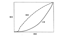
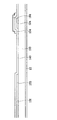
図1は、一般の液晶表示装置における様々な角度からのガンマ曲線を示したグラフで、C1は正面からのガンマ曲線、C2は上側方向からのガンマ曲線、C3は右側方向からのガンマ曲線、C4は対角方向からのガンマ曲線である。
Hereinafter, a structure of a liquid crystal display device according to an embodiment of the present invention and a thin film transistor array panel used therein will be described with reference to the drawings.
First, the principle of the present invention will be described in detail with reference to FIGS. 1 to 4B.
FIG. 1 is a graph showing gamma curves from various angles in a general liquid crystal display device, C1 is a gamma curve from the front, C2 is a gamma curve from the upper side, C3 is a gamma curve from the right side, C4 Is a gamma curve from the diagonal direction.
図1は、正面からのガンマ曲線とその他の方向からのガンマ曲線とにおいて大きな差があるガンマ歪曲現象を示す。即ち、同一な電圧を印加して同一な階調を表示しようとしても、正面と側面からの輝度差によって正面と側面からのイメージが異なる視認性の歪曲が発生する。特に、高諧調では、階調間の明るさの差のため更に酷い歪曲が発生する。
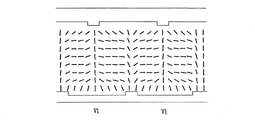
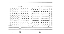
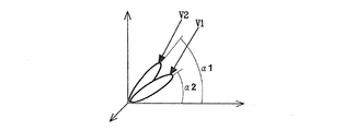
図2A、図2B、図3及び図4A、図4Bは、このような視認性問題を解決するための本発明の基本概念を示している。図2A及び図2Bは、一つの画素内に液晶分子の傾斜方向が異なる複数のドメインが形成されている液晶表示装置での液晶分子の配列を示す。図3は、図2Bの場合、電圧が異なる二つの領域での液晶分子の傾斜角を示す。図4Aは、図2Aに示した液晶表示装置における正面ガンマ曲線及び側面ガンマ曲線を示したグラフである。図4Bは、図2Bに示した液晶表示装置における正面ガンマ曲線及び側面ガンマ曲線を示したグラフである。
FIG. 1 shows the gamma distortion phenomenon in which there is a large difference between the gamma curve from the front and the gamma curve from other directions. In other words, even if the same voltage is applied to display the same gradation, visibility distortions in which the images from the front and the side are different due to the luminance difference between the front and the side are generated. In particular, in a high gradation, a more severe distortion occurs due to a difference in brightness between gradations.
2A, 2B, 3 and 4A, 4B show the basic concept of the present invention for solving such a visibility problem. 2A and 2B show an arrangement of liquid crystal molecules in a liquid crystal display device in which a plurality of domains having different tilt directions of liquid crystal molecules are formed in one pixel. FIG. 3 shows the tilt angles of liquid crystal molecules in two regions having different voltages in the case of FIG. 2B. FIG. 4A is a graph showing a front gamma curve and a side gamma curve in the liquid crystal display device shown in FIG. 2A. FIG. 4B is a graph showing a front gamma curve and a side gamma curve in the liquid crystal display device shown in FIG. 2B.
図2Aのように、一つの画素内に多重ドメインが存在しても、一つの画素内では、電場を生成する二つの電極の電位差が一定な場合には、図4Aに示すように、正面ガンマ曲線と側面ガンマ曲線との差が極めて大きい。
しかし、図2Bのように、二つの電界生成電極のうち一つの電極を二つの副電極に分けて互いに異なる電圧を印加すると、二つの副電極上の液晶層領域、つまり副領域にかかる電場の強さが変化し、そのため図3のように、二つの副領域内の液晶分子の傾斜角が異なるようになる。このようにして、図4Bのように、二つの副領域内の液晶分子の傾斜角差によって、側面からのガンマ曲線が正面からのガンマ曲線に近づく。その結果、正面と側面間の画面歪曲が減少し、視認性が優れた液晶表示装置を実現することができる。
As shown in FIG. 2A, even when multiple domains exist in one pixel, if the potential difference between two electrodes that generate an electric field is constant in one pixel, as shown in FIG. The difference between the curve and the side gamma curve is extremely large.
However, as shown in FIG. 2B, when one of the two electric field generating electrodes is divided into two sub-electrodes and different voltages are applied, the electric field applied to the liquid crystal layer region on the two sub-electrodes, that is, the sub-region, is reduced. The intensity changes, so that the tilt angles of the liquid crystal molecules in the two subregions become different as shown in FIG. In this way, as shown in FIG. 4B, the gamma curve from the side surface approaches the gamma curve from the front side due to the difference in tilt angle of the liquid crystal molecules in the two sub-regions. As a result, a screen distortion between the front and side surfaces can be reduced, and a liquid crystal display device with excellent visibility can be realized.
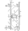
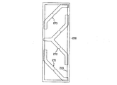
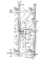
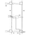
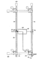
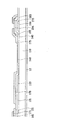
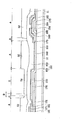
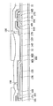
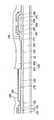
図7は、本発明の一実施形態による液晶表示装置用薄膜トランジスタ基板の配置図であり、図8は、本発明の一実施形態による液晶表示装置用カラーフィルター基板の配置図であり、図9は、本発明の一実施形態による液晶表示装置の配置図であり、図10は、図9に示す液晶表示装置をIV-IV´線に沿って切断した断面図である。
液晶表示装置は、下側の薄膜トランジスタ表示板100と、これと対向している上側の対向表示板200、及びこれらの間に形成され、二つの表示板100、200に対しほぼ垂直に配向されている液晶分子310を有する液晶層3からなる。この時、各々の表示板100、200の内側には、配向膜11、21が形成されており、配向膜11、21は、液晶層3の液晶分子310を表示板100、200に対し垂直に配向させる垂直配向モードであるのが好ましいが、そうでない場合もある。また、上部表示板200と下部表示板100の外側面には、各々上部及び下部偏光板12、22が付着されている。
FIG. 7 is a layout view of a thin film transistor substrate for a liquid crystal display according to an embodiment of the present invention, FIG. 8 is a layout view of a color filter substrate for a liquid crystal display according to an embodiment of the present invention, and FIG. FIG. 10 is a layout view of a liquid crystal display device according to an embodiment of the present invention, and FIG. 10 is a cross-sectional view of the liquid crystal display device shown in FIG. 9 cut along line IV-IV ′.
The liquid crystal display device includes a lower thin film
まず、下部の薄膜表示板は、次のような構成を有する。
ガラス等の透明な絶縁物質からなる絶縁基板110上に、ITO(indium tin oxide)やIZO(indium zinc oxide)等の透明な導電物質からなり、切開部191、193を通じて分離されている第1及び第2画素電極190a、190bが形成されている。第1画素電極190aは、薄膜トランジスタに接続されて画像信号電圧の印加を受け、第2画素電極190bは、第1画素電極190aと接続されている結合電極176と重畳することで、第1画素電極190aと電磁気的に結合(容量性結合)している。この時、薄膜トランジスタは、走査信号を伝達するゲート線121と画像信号を伝達するデータ線171に各々接続されて、走査信号に基づいて第1画素電極190aに印加される画像信号をオン(on)、オフ(off)する。第2画素電極190bは、切開部192を有する。前記第1及び第2画素電極190a、190bにおいて、反射型液晶表示装置の場合には、透明な物質からならないこともあり、その場合には、下部偏光板12も不要である。
First, the lower thin film display panel has the following configuration.
On the insulating
次に、上部対向表示板の構成は次の通りである。
ガラス等の透明な絶縁物質からなる絶縁基板210の下面に光漏れを防ぐためのブラックマトリックス220と、赤、緑、青のカラーフィルタ230、及びITOまたはIZO等の透明な導電物質からなる共通電極270が形成されている。ここで、共通電極270には、切開部271、272、273が形成されている。ブラックマトリックス220は、画素領域の周囲部のみならず共通電極270の切開部271、272、273と重畳する部分にも形成することができる。これは、切開部271、272、273のため生ずる光漏れを防ぐためである。
Next, the structure of the upper counter display panel is as follows.
A
次に、薄膜トランジスタ表示板100について更に詳細に説明する。
薄膜トランジスタ表示板100には、下部絶縁基板110上にゲート信号を伝達する複数のゲート線121が形成されている。ゲート線121は、主に横方向に延びており、各ゲート線121の一部は複数のゲート電極124をなす。ゲート線121には、ゲート電極124は突起状に形成され、本実施形態のように、ゲート線121は、外部からのゲート信号をゲート線121に伝達するための接触部を有することができる。この時、ゲート線121の端部129は、他の部分より広い幅を有するが、そうでない場合には、ゲート線121の端部は、基板110上部に直接形成されているゲート駆動回路の出力端に直接接続される。
Next, the thin film
In the thin film
ゲート線121と同一な層には、維持電極線131が横方向に延びて形成されており、各々の維持電極線131は、他の部分より広い幅を有する維持電極133を有する。
ゲート線121及び維持電極線131は、Al、Al合金、Ag、Ag合金、Cr、Ti、Ta、Mo等の金属で作られる。本実施形態のゲート線121及び維持電極線131は、単一層からなるが、物理化学的な特性が優れたCr、Mo、Ti、Ta等の金属層と、低い比抵抗のAl系またはAg系の金属層を含む二重層からなることもできる。その他にも様々な金属または導電体にてゲート線121及び維持電極線131を作ることができる。
In the same layer as the
The
ゲート線121及び維持電極線131の側面は傾斜しており、水平面に対する傾斜角は30〜80°であるのが好ましい。
ゲート線121及び維持電極線131の上には、窒化ケイ素(SiNx)等からなるゲート絶縁膜140が形成されている。
ゲート絶縁膜140上には、複数のデータ線171を始めとして複数のドレイン電極175が形成されている。各データ線171は、主に縦方向に延びており、各ドレイン電極175に向けて複数の枝を出して、データ線171から拡張したソース電極173を有する。データ線171の一端部に位置した接触部179は、外部からの画像信号をデータ線171に伝達する。
The side surfaces of the
A
A plurality of
また、データ線171と同一な層には、維持電極133と重畳して、ゲート絶縁膜140を介在してストレージキャパシタCst(図11参照)を構成する結合電極176が形成されている。この時、結合電極176は、ドレイン電極175から分離されているが、これら175、176は接続されていてもよい。この時、結合電極176は、維持電極133と重畳するように配置して、画素の開口率が減少するのを防ぐことができ、維持電極133の境界は、結合電極176の境界内に位置する。
Further, in the same layer as the
データ線171、ドレイン電極175及び結合電極176は、ゲート線121のように、クロム(Cr)、アルミニウム(Al)、モリブデン(Mo)、チタニウム(Ti)、タンタル(Ta)またはこれらの導電物質に素子の合金用金属を添加した(例:Al-Nd、Mo-N、Mo-Nb)合金で作ることができ、これらの単一膜またはこれらを含む多層膜(例:Mo/Al-Nd/Mo、Cr/Al)からなることができる。
The
データ線171、ドレイン電極175の下には、データ線171に沿って主に縦に長く延びた複数の線状半導体151が形成されている。非晶質シリコン等からなる各線状半導体151は、各ゲート電極124、ソース電極173及びドレイン電極175に向けて拡張されてチャンネル部154を有する。
半導体151とデータ線171及びドレイン電極175の間には、両者の接触抵抗をそれぞれ減少させるための複数の線状オーミック接触部材161及び島状のオーミック接触部材165が形成されている。オーミック接触部材161は、シリサイドやn型不純物が高濃度にドーピングされた非晶質シリコン等で作られ、枝として延びたオーミック接触部材163を有し、島状のオーミック接触部材165は、ゲート電極124を中心にオーミック接触部材163と対向する。
Under the
Between the
データ線171及びドレイン電極175の上には、平坦化特性が優れて感光性を有する有機物質、プラズマ化学気相蒸着(PECVD)で形成されるa-Si:C:O、a-Si:O:F等の低誘電率絶縁物質または窒化ケイ素等からなる保護膜180が形成されている。この時、保護膜180は、窒化ケイ素または酸化ケイ素からなる第1絶縁膜801と有機絶縁物質からなる第2絶縁膜802を含む。薄膜トランジスタ表示板100の上部に、赤、緑、青のカラーフィルタ230を形成する別の実施形態において、第2絶縁膜802は、赤、緑、青のカラーフィルタ230の絶縁層を有したり、これらをカラーフィルタ層で代替することができる。
On the
保護膜180には、ドレイン電極175の少なくとも一部とデータ線171の端部179をそれぞれ露出する複数のコンタクトホール(接触孔)182、185が備えられ、ゲート線121の端部129の一部を露出する複数のコンタクトホール181がゲート絶縁膜140と保護膜180を貫通している。また、保護膜180には、結合電極176を露出するコンタクトホール186が備えられているが、コンタクトホール186は、第1絶縁膜801に形成されており、第2絶縁膜802には、結合電極176上部の第1絶縁膜801を露出する開口部188が備えられている。
The
保護膜180上には、複数の画素電極を始めとして複数の接触補助部材81、82が形成されている。画素電極190a、190b及び接触補助部材81、82は、ITOやIZOのような透明導電体やアルミニウム(Al)のような光反射特性が優れた不透明導電体等で作られる。
複数の画素電極は、切開部191、193を通じて分離された第1画素電極190aと第2画素電極190bを含み、第1画素電極190aは、コンタクトホール186、185を通じてドレイン電極175及び結合電極176と接続され、第2画素電極190bは、結合電極176と重畳している。これにより、第2画素電極190bと結合電極176の間には、結合容量Ccp(図11参照)が形成され、これを通じて第2画素電極190bは、第1画素電極190aに電磁気的に結合(容量性結合)している。この時、第2画素電極190bは、開口部188を通じて露出した第1絶縁膜801のみを介在して結合電極176と重畳していて、これら190b、176の間では、狭い重畳面積で充分な結合容量を形成することができる。
A plurality of
The plurality of pixel electrodes include a
なお、第1または第2画素電極190a、190bと重畳して保持容量を形成する時に、第1画素電極190aと接続している結合電極176及び維持電極133は、ゲート絶縁膜140のみを介在して重畳していて、これら133、176の間では、狭い重畳面積で充分な保持容量を形成することができる。また、本実施形態のような構造によれば、結合容量及び保持容量を充分確保しながら結合電極176と維持電極133を重畳して配置することによって、画素の開口率を充分に確保できる。
Note that when the storage capacitor is formed so as to overlap with the first or
第1画素電極190aと第2画素電極190bを分ける境界は、ゲート線121に対し45°をなす部分191、193と垂直をなす部分とに分けられ、45°をなす二つの部分191、193が垂直をなす部分に比べて長さが長い。また、45°をなす二つの部分191、193は、互いに垂直をなしている。
第2画素電極190bは、切開部192を有し、切開部192は、第2画素電極190bの右側辺から左側辺に向けて切り込まれた形であり、入口は広く拡張されている。
The boundary between the
The
第1画素電極190a及び第2画素電極190bは、各々ゲート線121とデータ線171が交差して定義する画素領域を上下に二等分する線(ゲート線と平行な線)に対し実質的に鏡対称をなしている。
接触補助部材81、82は、各々コンタクトホール181、182を通じてゲート線の端部129とデータ線の端部179に接続している。
The
The
また、上部の絶縁基板210には、光漏れを防ぐためのブラックマトリクス220が形成されている。ブラックマトリックス220上には、赤、緑、青のカラーフィルタ230が形成されている。カラーフィルタ230上には、複数組の切開部271、272、273を有する共通電極270が形成されている。共通電極270は、ITOまたはIZO等の透明な導電体で形成する。
The upper insulating
共通電極270の一組の切開部271、272、273は、二つの画素電極190a、190bの境界のうちゲート線121に対し45°をなす部分191、193を介在し、これと平行な斜線部と画素電極190の辺と重畳する端部を有する。この時、端部は、縦方向端部と横方向端部に分類される。
この時、ドメイン規制手段である切開部271、272、273は、切り欠き形成されたノッチを有し、三角形、四角形、梯形、半円形であることができる。ノッチは、突き出た形や凹んだ形に形成することができる。図8に示す切開部271、272、273では、斜線部に三角形のノッチを設けている。
The pair of
At this time, the
ノッチは、切開部271、272、273に対応するドメイン境界に位置する液晶分子310の配列方向を決定する。従って、ドメインの境界に配列されている液晶分子310は、ノッチを通じて安定的かつ規則的に配列することができるので、ドメイン境界でムラや残像が発生するのを防ぎ、切開部271、272、273の幅を狭くして、輝度を増加させることができる。この時、ノッチは、一つのドメイン規制手段に一つまたは二つ以上を配置することができ、凹んだノッチ及び突き出たノッチを交互に複数配置することもできる。また、本実施形態では、共通電極270の切開部271、272、273にノッチを配置したが、画素電極190の切開部191、192、193にノッチを配置したり、薄膜トランジスタ表示板100または対向表示板200の両方に配置することもできる。
The notch determines the alignment direction of the
前記したような構造の薄膜トランジスタ表示板とカラーフィルタ表示板を整列して結合し、その間に液晶物質を注入して垂直配向すると、本発明の一実施形態による液晶表示装置の基本構造が完成する。
薄膜トランジスタ表示板とカラーフィルタ表示板を整列した時、共通電極270の一組の切開部271、272、273は、二つの画素電極190a、190bを各々複数の副領域(subarea)に区分するが、本実施形態では、図9に示したように、二つの画素電極190a、190bを各々4つの副領域に分ける。図9で、各副領域は、細長く形成されており、幅方向と長手方向が区別される。
When the thin film transistor array panel and the color filter display panel having the above-described structure are aligned and coupled, and a liquid crystal material is injected between them and vertically aligned, the basic structure of the liquid crystal display according to an embodiment of the present invention is completed.
When the thin film transistor array panel and the color filter display panel are aligned, the pair of
画素電極190a、190bの各副領域とこれに対応する基準電極270の各副領域との間にある液晶層3部分を以下で小領域(subregion)と記載し、これらの小領域は、電界印加時にその内部に位置する液晶分子の平均長軸方向によって4種類に分類され、以下でこれをドメイン(domain)と記載する。
このような構造の液晶表示装置において、第1画素電極190aは、薄膜トランジスタを通じて画像信号電圧の印加を受けるのに対し、第2画素電極190bは、結合電極176との容量性結合によって電圧が変動するので、第2画素電極190bの電圧は、第1画素電極190bの電圧に比べて絶対値が常に低い。このように、一つの画素領域内に電圧が異なる二つの画素電極を配置すると、二つの画素電極を通じて互いに異なるガンマ曲線が形成され、このようなガンマ曲線は、互いに補償して、ガンマ曲線の歪曲を減少させることができ、これによって優れた視認性を確保できる。
The portion of the
In the liquid crystal display device having such a structure, the image signal voltage is applied to the
また、本実施形態では、結合電極とドレイン電極が分離されているが、結合電極は、ドレイン電極と同じ導電層で接続されることができ、結合電極が第2画素電極とコンタクトホールで接続されて、第1画素電極と重畳してキャパシタを構成しても、視認性改善効果を得ることができる。そして、本実施形態では、維持電極及び維持電極線を別途設けているが、別途の維持電極の代わりに、ゲート線やデータ線を用いることもできる。 In this embodiment, the coupling electrode and the drain electrode are separated, but the coupling electrode can be connected by the same conductive layer as the drain electrode, and the coupling electrode is connected to the second pixel electrode by a contact hole. Even if the capacitor is formed so as to overlap with the first pixel electrode, the effect of improving the visibility can be obtained. In this embodiment, the storage electrode and the storage electrode line are separately provided. However, a gate line or a data line can be used instead of the separate storage electrode.
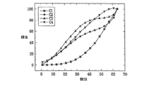
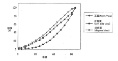
図5は、本実施形態の適用結果を示すガンマ曲線である。同図によれば、約0〜30階調では、正面と側面のガンマ曲線が密着し、高諧調では、正面と側面の階調間輝度差が改善したことが分かる。
本発明の他の実施形態として、一つの画素内に互いに異なる電圧値を有する液晶キャパシタを3つ以上、つまり一つの画素内の液晶層が互いに異なる強さを有する電場の印加を受ける3つ以上の副領域を形成する場合にも適用することができる。ここで、副領域の数は、実際の表示装置を設計する時、開口率及び画素の大きさ等の設計規則に従って最適に決定する。
FIG. 5 is a gamma curve showing the application result of this embodiment. According to the figure, it can be seen that the front and side gamma curves are in close contact with each other at about 0 to 30 gradations, and the luminance difference between the front and side gradations is improved in high gradation.
As another embodiment of the present invention, three or more liquid crystal capacitors having different voltage values in one pixel, that is, three or more liquid crystal layers in one pixel are applied with electric fields having different strengths. The present invention can also be applied to the case where the subregion is formed. Here, when designing an actual display device, the number of sub-regions is optimally determined according to design rules such as an aperture ratio and a pixel size.
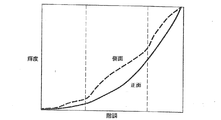
図6は、3つの副領域を有する液晶表示装置の正面及び側面ガンマ曲線を示したグラフで、二つの副領域を有する場合よりも側面ガンマ曲線がより正面ガンマ曲線に近いことが分かる。
次に、第1画素電極190aの電圧が第2画素電極190bの電圧より低く維持される理由を図11を参照して説明する。
FIG. 6 is a graph showing the front and side gamma curves of a liquid crystal display device having three sub-regions, and it can be seen that the side gamma curve is closer to the front gamma curve than the case of having two sub-regions.
Next, the reason why the voltage of the
図11は、本発明の第1実施形態による液晶表示装置の回路図である。
図11でClcaは、第1画素電極190aと共通電極270の間で形成される液晶容量を示し、Cstは、第1画素電極190aと維持電極線131の間で形成される保持容量を示す。Clcbは、第2画素電極190bと共通電極270の間で形成される液晶容量を示し、Ccpは、第1画素電極190aに接続された結合電極176と第2画素電極190bの間で形成される結合容量を示す。
FIG. 11 is a circuit diagram of the liquid crystal display device according to the first embodiment of the present invention.
In FIG. 11, Clca indicates a liquid crystal capacitance formed between the
共通電極270電圧に対する第1画素電極190aの電圧をVaとし、第2画素電極190bの電圧をVbとするとき、電圧法則に従って、
Vb=Va×[Ccp/(Ccp+Clcb)]
であり、Ccp/(Ccp+Clcb)は、常に1より小さいので、VbはVaに比べて常に小さい。
When the voltage of the
Vb = Va × [Ccp / (Ccp + Clcb)]
Since Ccp / (Ccp + Clcb) is always smaller than 1, Vb is always smaller than Va.
一方、Ccpを調節することによって、Vaに対するVbの比率を調整することができる。Ccpの調節は、結合電極176と第2画素電極190bの重畳面積及び距離を調整することによって可能である。重畳面積は、結合電極176の幅を変化させることによって容易に調整でき、距離は、結合電極176の形成位置を変化させることによって調整することができる。即ち、本発明の実施形態では、結合電極176をデータ線171と同一層に形成したが、ゲート線121と同一層に形成したり、第2画素電極と結合電極の間に第2保護膜を除去しないで残すことによって、結合電極176と第2画素電極190bとの間の距離を増加させることができる。
On the other hand, the ratio of Vb to Va can be adjusted by adjusting Ccp. Ccp can be adjusted by adjusting the overlapping area and distance between the
以下、図7、図9及び図10に示した液晶表示装置用薄膜トランジスタ表示板を本発明の一実施形態によって製造する方法について、図12A乃至図17B、図7、図9及び図10を参照して詳細に説明する。
図12A、図13A、図14A及び図16Aは、図7乃至図10に示した液晶表示装置の薄膜トランジスタ表示板を本発明の一実施形態によって製造する方法の中間段階における配置図で、その工程順で示したものであり、図12Bは、図12Aに示した薄膜トランジスタ表示板をVIb-VIb´線に沿って切断した断面図であり、図13Bは、図13Aに示した薄膜トランジスタ表示板をVIIb-VIIb´線に沿って切断した断面図であり、図14Bは、図14Aに示した薄膜トランジスタ表示板をVIIIb-VIIIb´線に沿って切断した断面図であり、図15は、図14Aに示した薄膜トランジスタ表示板をVIIIb-VIIIb´線に沿って切断した断面図で、図14Bに続く工程を示すものであり、図16Bは、図16Aに示した薄膜トランジスタ表示板をXb-Xb´線に沿って切断した断面図で、図15に続く工程を示すものであり、図17は、図16Aに示した薄膜トランジスタ表示板をXb-Xb´線に沿って切断した断面図で、図16Bに続く工程を示すものである。
Hereinafter, a method of manufacturing the thin film transistor array panel for a liquid crystal display device shown in FIGS. 7, 9 and 10 according to an embodiment of the present invention will be described with reference to FIGS. 12A to 17B, FIGS. Will be described in detail.
12A, 13A, 14A, and 16A are layout diagrams in an intermediate stage of a method of manufacturing the thin film transistor array panel of the liquid crystal display device shown in FIGS. 7 to 10 according to an embodiment of the present invention. 12B is a cross-sectional view of the thin film transistor array panel shown in FIG. 12A cut along the line VIb-VIb ′. FIG. 13B is a cross-sectional view of the thin film transistor array panel shown in FIG. 14B is a cross-sectional view taken along the line VIIb ′, FIG. 14B is a cross-sectional view taken along the line VIIIb-VIIIb ′ of the thin film transistor array panel shown in FIG. 14A, and FIG. 15 is shown in FIG. 14A. FIG. 16B is a cross-sectional view of the thin film transistor array panel cut along the line VIIIb-VIIIb ′, showing the process following FIG. 14B. FIG. FIG. 17 is a cross-sectional view of the thin film transistor array panel cut along the line Xb-Xb ′, illustrating a process following FIG. 15, and FIG. 17 illustrates the thin film transistor array panel illustrated in FIG. 16A along the line Xb-Xb ′. FIG. 16B is a cross-sectional view taken along the line showing a step subsequent to FIG. 16B.
まず、透明なガラス等で作られた絶縁基板110上に、二つの層の金属膜をスパッタリング法等で順に積層する。この時、金属膜は、IZOまたはITOとの接触特性が優れた金属、例えばモリブデン、モリブデン合金、またはクロム等の下部膜及びアルミニウム系金属からなる上部膜で積層することができる。
次に、図12A及び図12Bに示したように、感光膜パターンを用いたフォトエッチング工程で金属膜をパターニングして、複数のゲート電極124を含むゲート線121と、複数の維持電極133を含む維持電極線131を形成する。
First, two layers of metal films are sequentially laminated on an insulating
Next, as shown in FIGS. 12A and 12B, the metal film is patterned by a photo-etching process using a photosensitive film pattern to include a
図13A及び図13Bに示したように、ゲート絶縁膜140、真性非晶質シリコン層、不純物非晶質シリコン層の3層膜を連続して積層する。次に、不純物非晶質シリコン層及び真性非晶質シリコン層をフォトエッチングして、複数の線状不純物半導体164及び複数の突出部154を各々含む線状真性半導体151を形成する。ゲート絶縁膜140の材料には、窒化ケイ素が良く、積層温度は250〜500℃、厚さは2,000〜5,000Å程度が好ましい。
As shown in FIGS. 13A and 13B, a three-layer film of a
次に、前記した導電物質をスパッタリング法等で順に積層して金属膜を形成した後、図14A及び図14Bに示したように、金属膜を順にパターニングして、複数の結合電極176と複数のソース電極173を各々含む複数のデータ線171及び複数のドレイン電極175を形成する。
次に、データ線171及びドレイン電極175の上部の感光膜を除去するか、そのままにした状態で、データ線171、ドレイン電極175及び結合電極176で覆われないで露出された不純物半導体164の一部を除去することによって、複数の突出部163を各々含む複数の線状オーミック接触部材161と複数の島状オーミック接触部材165を完成する一方、その下の真性半導体151部分を露出させる。
Next, after forming the metal film by sequentially laminating the above-described conductive materials by a sputtering method or the like, as shown in FIGS. 14A and 14B, the metal film is patterned in order to form a plurality of
Next, the photosensitive film over the
次に、真性半導体151部分の表面を安定化するために、酸素プラズマ処理を引き続き実施するのが好ましい。
次に、図15のように、窒化ケイ素のような無機絶縁膜の第1絶縁膜801及び低誘電率を有する有機絶縁膜の第2絶縁膜802を順に積層して保護膜180を形成し、その上部に感光膜をスピンコーティング法で塗布した後、マスクを用いるフォト工程で感光膜パターン52、54を形成する。
Next, in order to stabilize the surface of the
Next, as shown in FIG. 15, a
ここで、現像された感光膜の厚さは位置によって異なっており、感光膜は、厚さが次第に薄くなる第1乃至第3部分からなる。A領域(以下、その他の領域)に位置した第1部分と、C領域(以下、結合領域)に位置した第2部分は、各々図面符号52と54で示す。B領域(以下、接触領域)に位置した第3部分には、感光膜が残っておらず、第2絶縁膜802が露出している。
Here, the thickness of the developed photosensitive film varies depending on the position, and the photosensitive film is composed of first to third portions whose thickness is gradually reduced. A first part located in the A area (hereinafter referred to as other area) and a second part located in the C area (hereinafter referred to as coupling area) are indicated by
このように、位置によって感光膜の厚さを異ならせる方法は様々であって、露光マスクに透明領域と遮光領域のみならず半透明領域を設けることがその一例である。半透明領域には、スリットパターン、格子パターンまたは透過率が中間であるか、厚さが中間である薄膜が備えられる。
次に、図16A及び図16Bに示したように、感光膜パターン52、54をエッチングマスクとして、第2絶縁膜802と第1絶縁膜801を順にエッチングして、ドレイン電極175及び結合電極176を各々露出するコンタクトホール185、186を形成する。この時、ゲート線121及びデータ線171各々の端部129、179を露出するコンタクトホール181、82も同時に形成する。次に、結合領域Cに残っている第2部分54をアッシングで除去する。
As described above, there are various methods for varying the thickness of the photosensitive film depending on the position, and one example is to provide not only a transparent area and a light-shielding area but also a translucent area on the exposure mask. The translucent region is provided with a slit pattern, a lattice pattern, or a thin film having an intermediate transmittance or an intermediate thickness.
Next, as shown in FIGS. 16A and 16B, the second
次に、図17に示したように、結合領域Cで露出した第2絶縁膜802の一部をエッチングして、第2絶縁膜802に開口部188を形成する。
この時、第2絶縁膜802を感光性有機絶縁物質で形成する他の実施形態では、第2絶縁膜802を感光膜パターン52、54と共に形成した後、前記した工程順に沿ってエッチング工程を行う。
Next, as shown in FIG. 17, a part of the second
At this time, in another embodiment in which the second
最後に、図7、図9及び図10に示したように、500Å乃至1,500Å厚さのIZOまたはITO層をスパッタリング法で蒸着しフォトエッチングして、複数の画素電極190a、190b及び複数の接触補助部材81、82を形成する。IZO層を使用する場合のエッチングは、(HNO3/(NH4)2Ce(NO3)6/H2O)等のクロム用エッチング液を使用する湿式エッチング法が好ましいが、このエッチング液は、アルミニウムを腐食させないので、データ線171、ドレイン電極175、ゲート線121でアルミニウム導電膜が腐食するのを防ぐことができる。
Finally, as shown in FIGS. 7, 9 and 10, an IZO or ITO layer having a thickness of 500 to 1,500 mm is deposited by sputtering and photoetched to form a plurality of
なお、本発明の他の実施形態による液晶表示装置で薄膜トランジスタ表示板は、別の構造を有することができる。これについて図面を参照して詳しく説明する。
図18は、本発明の他の実施形態による液晶表示装置の構造を示した配置図であり、図19は、図18に示す液晶表示装置をXII-XII´線に沿って切断した断面図である。
In addition, the thin film transistor array panel in the liquid crystal display according to another embodiment of the present invention may have another structure. This will be described in detail with reference to the drawings.
18 is a layout view showing a structure of a liquid crystal display device according to another embodiment of the present invention, and FIG. 19 is a cross-sectional view of the liquid crystal display device shown in FIG. 18 cut along the line XII-XII ′. is there.
図18乃至図19のように、本実施形態による液晶表示装置用薄膜トランジスタ表示板の層状構造は、図7、図9及び図10に示した液晶表示装置用薄膜トランジスタ表示板の層状構造とほぼ同様である。即ち、基板110上に複数のゲート電極124を含む複数のゲート線121が形成され、その上にゲート絶縁膜140、複数の突出部154を含む複数の線状半導体151、複数の突出部163を各々含む複数の線状オーミック接触部材161及び複数の島状オーミック接触部材165が順に形成されている。オーミック接触部材161、165及びゲート絶縁膜140の上には、複数のソース電極153を含む複数のデータ線171、複数のドレイン電極175、複数の結合電極176が形成され、その上に第1絶縁膜801及び第2絶縁膜802を含む保護膜180が形成されている。保護膜180及び/またはゲート絶縁膜140には、複数のコンタクトホール182、185、186、181が形成され、保護膜180上には複数の画素電極190a、190bと複数の接触補助部材81、82が形成されている。
As shown in FIGS. 18 to 19, the layered structure of the thin film transistor array panel for the liquid crystal display according to the present embodiment is substantially the same as the layered structure of the thin film transistor array panel for the liquid crystal display shown in FIGS. 7, 9 and 10. is there. That is, a plurality of
しかし、図7、図9及び図10に示した薄膜トランジスタ表示板と異なって、本実施形態による薄膜トランジスタ表示板において、半導体151は、薄膜トランジスタが位置する突出部154を除けば、データ線171、ドレイン電極175及びその下部のオーミック接触部材161、165と実質的に同一な平面形態を有する。より詳細には、線状半導体151は、データ線171及びドレイン電極175とその下部のオーミック接触部材161、165の下に存在する部分以外にも、ソース電極173とドレイン電極175の間に、これらで覆われず露出する部分を有している。
However, unlike the thin film transistor array panel shown in FIGS. 7, 9 and 10, in the thin film transistor array panel according to the present embodiment, the
勿論このような本実施形態による液晶表示装置用薄膜トランジスタ表示板は、結合電極176を有しており、結合電極176の下部には非晶質シリコン層156、166が同一な模様で形成されている。
このような薄膜トランジスタ表示板の製造方法では、保護膜190をパターニングする時と同様に、部分的に厚さが異なる感光膜パターンを形成する。このような感光膜パターンは、厚さが次第に薄くなる第1乃至第3部分からなる。これを図15と比較して説明すると、第1部分は配線領域に対応し、第2部分はチャンネル領域に対応し、各々図面符号52と54に対応する。次に、一連のエッチング段階によって、複数のソース電極173を各々含む複数のデータ線171、複数のドレイン電極175及び結合電極176を形成し、複数の突出部163を各々含む複数の線状オーミック接触部材161及び複数の島状オーミック接触部材165、並びに複数の突出部154を含む複数の線状半導体151を形成する。
Of course, the thin film transistor array panel for the liquid crystal display according to the present embodiment has a
In such a method for manufacturing a thin film transistor array panel, photosensitive film patterns having partially different thicknesses are formed in the same manner as when the protective film 190 is patterned. Such a photosensitive film pattern includes first to third portions whose thickness is gradually reduced. This will be described in comparison with FIG. 15. The first portion corresponds to the wiring region, the second portion corresponds to the channel region, and corresponds to the
以上のような構成を通じて液晶表示装置の側面視認性を向上して視野角を拡張することができる。また、保持容量を形成する時、ゲート絶縁膜のみを介在して維持電極と結合電極を重畳させ、結合容量を形成する時、保護膜の一部のみを介在してサブ画素電極と結合電極を重畳させ、狭い重畳面積で維持容量及び結合容量を充分に確保することによって、画素の開口率を確保できる。 Through the above configuration, the side visibility of the liquid crystal display device can be improved and the viewing angle can be expanded. Further, when forming the storage capacitor, the sustain electrode and the coupling electrode are overlapped with each other only through the gate insulating film, and when forming the coupling capacitor, the sub-pixel electrode and the coupling electrode are interposed only through a part of the protective film. The aperture ratio of the pixel can be ensured by overlapping and sufficiently securing the storage capacitor and the coupling capacitor with a small overlapping area.
以上で、本発明の好適な実施形態について詳細に説明したが、本発明の権利範囲はこれに限定されるものでなく、特許請求の範囲で定義している本発明の基本概念を利用した当業者の様々な変形及び改良形態も本発明の権利範囲に属するものである。特に、画素電極及び共通電極に形成する切開部の配置は多様に変形可能である。 The preferred embodiment of the present invention has been described in detail above. However, the scope of the present invention is not limited to this, and the basic concept of the present invention defined in the claims is used. Various modifications and improvements of the traders are also within the scope of the present invention. In particular, the arrangement of the cutouts formed in the pixel electrode and the common electrode can be variously modified.
121 ゲート線
124 ゲート電極
131 維持電極線
133 維持電極
151、154 半導体
161、163、165 オーミック接触部材
176 結合電極
171 データ線
173 ソース電極
175 ドレイン電極
190 画素電極
191、192、193 切開部
270 対向電極
271、272、273 切開部
801、802 第1及び第2保護膜
121
Claims (22)
前記絶縁基板上に形成されている第1信号線と、
前記第1信号線と絶縁して交差している第2信号線と、
前記第1信号線と前記第2信号線が交差して定義する各画素領域毎に形成されている第1画素電極と、
前記第1信号線、前記第2信号線及び第1画素電極に3端子がそれぞれ接続されている薄膜トランジスタと、
前記画素領域毎に形成され、前記第1画素電極に容量性結合している少なくとも一つ以上の第2画素電極と、
前記第1画素電極と接続され、前記第2画素電極と重畳する結合電極と、
前記第1及び第2画素電極と前記結合電極との間に形成され、少なくとも前記第2画素電極と重畳する一部が他の部分より薄い厚さを有する保護膜と、
を備える薄膜トランジスタ表示板。 An insulating substrate;
A first signal line formed on the insulating substrate;
A second signal line insulated from and intersecting the first signal line;
A first pixel electrode formed for each pixel region defined by intersecting the first signal line and the second signal line;
Thin film transistors having three terminals connected to the first signal line, the second signal line, and the first pixel electrode,
At least one second pixel electrode formed for each pixel region and capacitively coupled to the first pixel electrode;
A coupling electrode connected to the first pixel electrode and overlapping the second pixel electrode;
A protective film formed between the first and second pixel electrodes and the coupling electrode, and at least a portion overlapping the second pixel electrode has a thickness smaller than that of the other portion;
A thin film transistor array panel comprising:
前記第1信号線と絶縁して交差している第2信号線を形成する段階、
前記第1信号線と前記第2信号線が交差して定義する各画素領域毎に第1画素電極及び第2画素電極を形成する段階、
前記第1画素電極と接続され、前記第2画素電極と重畳する結合電極を形成する段階、
前記第1画素電極及び第2画素電極と前記結合電極の間に保護膜を形成する段階を含み、
前記第1及び第2画素電極と前記結合電極の間に形成された保護膜は、前記第2画素電極と前記結合電極が重畳する部分で少なくとも一部が他の部分の保護膜より薄い厚さを有するようにする薄膜トランジスタ表示板の製造方法。 Forming a first signal line on an insulating substrate;
Forming a second signal line that is insulated from and intersects the first signal line;
Forming a first pixel electrode and a second pixel electrode for each pixel region defined by crossing the first signal line and the second signal line;
Forming a coupling electrode connected to the first pixel electrode and overlapping the second pixel electrode;
Forming a protective film between the first and second pixel electrodes and the coupling electrode;
The protective film formed between the first and second pixel electrodes and the coupling electrode is a portion where the second pixel electrode and the coupling electrode overlap with each other, and at least a part is thinner than the protective film of the other part. A method for manufacturing a thin film transistor array panel.
前記絶縁基板上に形成されているゲート配線と、
前記ゲート配線上に形成されているゲート絶縁膜と、
前記ゲート絶縁膜上に形成されているデータ配線及び結合電極と、
前記データ配線及び結合電極上に形成されている第1保護膜及び第2保護膜と、
前記ゲート配線とデータ配線が交差して定義される画素領域と、
前記画素領域に形成された第1画素電極及び第2画素電極と、
前記第2画素電極と結合電極が重畳する位置で前記第2保護膜に形成されている開口部と、
対向基板と、
前記対向基板に形成され、開口部を有する共通電極と、
前記絶縁基板と対向基板との間に注入されている液晶層と、
を備える液晶表示装置。 An insulating substrate;
A gate wiring formed on the insulating substrate;
A gate insulating film formed on the gate wiring;
A data line and a coupling electrode formed on the gate insulating film;
A first protective film and a second protective film formed on the data line and the coupling electrode;
A pixel region defined by intersecting the gate wiring and the data wiring;
A first pixel electrode and a second pixel electrode formed in the pixel region;
An opening formed in the second protective film at a position where the second pixel electrode and the coupling electrode overlap;
A counter substrate;
A common electrode formed on the counter substrate and having an opening;
A liquid crystal layer injected between the insulating substrate and the counter substrate;
A liquid crystal display device comprising:
Applications Claiming Priority (2)
| Application Number | Priority Date | Filing Date | Title |
|---|---|---|---|
| KR1020040052565A KR101100878B1 (en) | 2004-07-07 | 2004-07-07 | Liquid crystal display having multi domain and panel for the same |
| KR1020040053395A KR101100877B1 (en) | 2004-07-09 | 2004-07-09 | Display device having multi domain and panel for the same |
Related Child Applications (1)
| Application Number | Title | Priority Date | Filing Date |
|---|---|---|---|
| JP2009092192A Division JP4999875B2 (en) | 2004-07-07 | 2009-04-06 | Multi-domain liquid crystal display device |
Publications (2)
| Publication Number | Publication Date |
|---|---|
| JP2006023744A true JP2006023744A (en) | 2006-01-26 |
| JP2006023744A5 JP2006023744A5 (en) | 2008-04-17 |
Family
ID=35731703
Family Applications (2)
| Application Number | Title | Priority Date | Filing Date |
|---|---|---|---|
| JP2005198345A Pending JP2006023744A (en) | 2004-07-07 | 2005-07-07 | Multi-domain liquid crystal display and display plate used for the same |
| JP2009092192A Expired - Fee Related JP4999875B2 (en) | 2004-07-07 | 2009-04-06 | Multi-domain liquid crystal display device |
Family Applications After (1)
| Application Number | Title | Priority Date | Filing Date |
|---|---|---|---|
| JP2009092192A Expired - Fee Related JP4999875B2 (en) | 2004-07-07 | 2009-04-06 | Multi-domain liquid crystal display device |
Country Status (3)
| Country | Link |
|---|---|
| US (1) | US7834945B2 (en) |
| JP (2) | JP2006023744A (en) |
| TW (1) | TWI379113B (en) |
Cited By (4)
| Publication number | Priority date | Publication date | Assignee | Title |
|---|---|---|---|---|
| JP2007316641A (en) * | 2006-05-24 | 2007-12-06 | Samsung Electronics Co Ltd | Display substrate and method for manufacturing the same, and liquid crystal display device having the same |
| WO2010052963A1 (en) * | 2008-11-05 | 2010-05-14 | シャープ株式会社 | Active matrix substrate, liquid crystal panel, liquid crystal display unit, liquid crystal display device, and television receiver |
| WO2010137230A1 (en) * | 2009-05-25 | 2010-12-02 | シャープ株式会社 | Active matrix substrate, liquid crystal panel, liquid crystal display device, and television receiver |
| JP2012208518A (en) * | 2006-05-24 | 2012-10-25 | Samsung Electronics Co Ltd | Display substrate, method for manufacturing the same, and liquid crystal display device including the same |
Families Citing this family (6)
| Publication number | Priority date | Publication date | Assignee | Title |
|---|---|---|---|---|
| US7526463B2 (en) * | 2005-05-13 | 2009-04-28 | Rockwell Automation Technologies, Inc. | Neural network using spatially dependent data for controlling a web-based process |
| KR101427708B1 (en) * | 2007-02-01 | 2014-08-11 | 삼성디스플레이 주식회사 | Liquid crystal display panel |
| KR20100007081A (en) | 2008-07-11 | 2010-01-22 | 삼성전자주식회사 | Display substrate and display panel having the same |
| KR20100024639A (en) * | 2008-08-26 | 2010-03-08 | 삼성전자주식회사 | Liquid crystal display |
| KR101830274B1 (en) | 2011-01-28 | 2018-02-21 | 삼성디스플레이 주식회사 | Liquid crystal display |
| CN103022150B (en) * | 2012-12-25 | 2015-05-20 | 京东方科技集团股份有限公司 | Thin film transistor, method for manufacturing same, array substrate and display device |
Family Cites Families (22)
| Publication number | Priority date | Publication date | Assignee | Title |
|---|---|---|---|---|
| JP3092537B2 (en) * | 1997-01-24 | 2000-09-25 | 日本電気株式会社 | Liquid crystal display |
| JP3782194B2 (en) * | 1997-02-28 | 2006-06-07 | 株式会社東芝 | Active matrix liquid crystal display device |
| JPH10268794A (en) | 1997-03-26 | 1998-10-09 | Sharp Corp | Display panel |
| US6034414A (en) * | 1997-11-18 | 2000-03-07 | Industrial Technology Research Institute | Variable capacitor using resistor generated heat to control dielectric thickness |
| KR100333179B1 (en) * | 1998-06-30 | 2002-08-24 | 주식회사 현대 디스플레이 테크놀로지 | Thin film transistor liquid crystal display device and manufacturing method thereof |
| KR100381054B1 (en) * | 1999-12-28 | 2003-04-18 | 엘지.필립스 엘시디 주식회사 | Transparent Electrode Composed of Indium-Zinc-Oxide and Etchant For Etching The Same |
| JP4357689B2 (en) * | 2000-03-28 | 2009-11-04 | シャープ株式会社 | Liquid crystal display panel and manufacturing method thereof |
| JP2001324725A (en) * | 2000-05-12 | 2001-11-22 | Hitachi Ltd | Liquid crystal display device and method of manufacture |
| US6690594B2 (en) * | 2000-08-10 | 2004-02-10 | Sal G. Amarillas | Electrical power conservation apparatus and method |
| KR100380141B1 (en) * | 2000-09-25 | 2003-04-11 | 엘지.필립스 엘시디 주식회사 | array panel for liquid crystal display and fabricating method of the same |
| KR100587217B1 (en) * | 2000-12-29 | 2006-06-08 | 엘지.필립스 엘시디 주식회사 | A substrate for IPS mode Liquid crystal display device and method for fabricating the same |
| TW513604B (en) * | 2001-02-14 | 2002-12-11 | Au Optronics Corp | A thin film transistor liquid crystal display |
| WO2003044595A1 (en) | 2001-11-22 | 2003-05-30 | Samsung Electronics Co., Ltd. | Liquid crystal display and thin film transistor array panel |
| KR100840326B1 (en) * | 2002-06-28 | 2008-06-20 | 삼성전자주식회사 | a liquid crystal display and a thin film transistor array panel for the same |
| KR100870016B1 (en) * | 2002-08-21 | 2008-11-21 | 삼성전자주식회사 | A thin film transistor array panel, a liquid crystal display including the panel |
| KR100878241B1 (en) | 2002-09-27 | 2009-01-13 | 삼성전자주식회사 | Thin film transistor substrate for multi-domain liquid crystal display |
| KR100890026B1 (en) * | 2002-11-20 | 2009-03-25 | 삼성전자주식회사 | Apparatus of driving liquid crystal display and method thereof |
| US7019805B2 (en) * | 2002-12-31 | 2006-03-28 | Lg.Philips Lcd Co., Ltd. | Liquid crystal display device having a multi-domain structure and a manufacturing method for the same |
| KR100961941B1 (en) * | 2003-01-03 | 2010-06-08 | 삼성전자주식회사 | Thin film transistor array panel for multi-domain liquid crystal display |
| KR100935670B1 (en) * | 2003-04-04 | 2010-01-07 | 삼성전자주식회사 | Liquid crystal display, thin film transistor array panel and method for manufacturing the same |
| KR100569718B1 (en) * | 2003-05-20 | 2006-04-10 | 삼성전자주식회사 | Multi-domain liquid crystal display |
| KR20040105934A (en) * | 2003-06-10 | 2004-12-17 | 삼성전자주식회사 | Liquid crystal display having multi domain and panel for the same |
-
2005
- 2005-06-30 TW TW094122088A patent/TWI379113B/en not_active IP Right Cessation
- 2005-07-07 US US11/175,254 patent/US7834945B2/en not_active Expired - Fee Related
- 2005-07-07 JP JP2005198345A patent/JP2006023744A/en active Pending
-
2009
- 2009-04-06 JP JP2009092192A patent/JP4999875B2/en not_active Expired - Fee Related
Cited By (10)
| Publication number | Priority date | Publication date | Assignee | Title |
|---|---|---|---|---|
| JP2007316641A (en) * | 2006-05-24 | 2007-12-06 | Samsung Electronics Co Ltd | Display substrate and method for manufacturing the same, and liquid crystal display device having the same |
| JP2012208518A (en) * | 2006-05-24 | 2012-10-25 | Samsung Electronics Co Ltd | Display substrate, method for manufacturing the same, and liquid crystal display device including the same |
| KR101294269B1 (en) * | 2006-05-24 | 2013-08-08 | 삼성디스플레이 주식회사 | Display Substrate And Method of Fabricating The Same And Liquid Crystal Display Apparatus Having The Same |
| KR101341060B1 (en) * | 2006-05-24 | 2013-12-13 | 삼성디스플레이 주식회사 | Display Substrate And Method of Fabricating The Same And Liquid Crystal Display Apparatus Having The Same |
| WO2010052963A1 (en) * | 2008-11-05 | 2010-05-14 | シャープ株式会社 | Active matrix substrate, liquid crystal panel, liquid crystal display unit, liquid crystal display device, and television receiver |
| CN102203663A (en) * | 2008-11-05 | 2011-09-28 | 夏普株式会社 | Active matrix substrate, liquid crystal panel, liquid crystal display unit, liquid crystal display device, and television receiver |
| US8514339B2 (en) | 2008-11-05 | 2013-08-20 | Sharp Kabushiki Kaisha | Active matrix substrate, liquid crystal panel, liquid crystal display unit, liquid crystal display device, and television receiver |
| JP5323856B2 (en) * | 2008-11-05 | 2013-10-23 | シャープ株式会社 | Active matrix substrate, liquid crystal panel, liquid crystal display unit, liquid crystal display device, television receiver |
| WO2010137230A1 (en) * | 2009-05-25 | 2010-12-02 | シャープ株式会社 | Active matrix substrate, liquid crystal panel, liquid crystal display device, and television receiver |
| US8665202B2 (en) | 2009-05-25 | 2014-03-04 | Sharp Kabushiki Kaisha | Active matrix substrate, liquid crystal panel, liquid crystal display device, and television receiver |
Also Published As
| Publication number | Publication date |
|---|---|
| US20060023134A1 (en) | 2006-02-02 |
| JP4999875B2 (en) | 2012-08-15 |
| US7834945B2 (en) | 2010-11-16 |
| TWI379113B (en) | 2012-12-11 |
| TW200606510A (en) | 2006-02-16 |
| JP2009151343A (en) | 2009-07-09 |
Similar Documents
| Publication | Publication Date | Title |
|---|---|---|
| JP4999875B2 (en) | Multi-domain liquid crystal display device | |
| JP4815584B2 (en) | Liquid crystal display device and thin film transistor display panel used therefor | |
| KR101112539B1 (en) | Liquid crystal display having multi domain and panel for the same | |
| JP4953416B2 (en) | Liquid crystal display | |
| JP5025129B2 (en) | Thin film transistor display panel | |
| JP5132894B2 (en) | Display board and liquid crystal display device including the same | |
| US9335600B2 (en) | Liquid crystal display device and method for fabricating the same | |
| JP4826979B2 (en) | Thin film transistor display panel and liquid crystal display device including the same | |
| US8085353B2 (en) | Thin film transistor array panel having a pixel electrode including a first subpixel electrode and a second subpixel electrode connected to the drain electrode of the thin film transistor and a third subpixel electrode capacitively coupled to a coupling electrode extended from the drain electrode | |
| JP4914614B2 (en) | Thin film transistor array panel, liquid crystal display device including the same, and manufacturing method thereof | |
| US7999880B2 (en) | Thin film transistor array panel and manufacturing method thereof | |
| US20090102994A1 (en) | In-plane switching mode liquid crystal display and method for fabricating the same | |
| JP2005062882A (en) | Multi-domain liquid crystal display device and display plate used for the same | |
| JP2006023744A5 (en) | ||
| TWI390317B (en) | Liquid crystal display and thin film transistor array panel thereof | |
| US7460192B2 (en) | Liquid crystal display, thin film diode panel, and manufacturing method of the same | |
| JP2004341526A (en) | Thin film transistor display panel and multidomain liquid crystal display containing the same | |
| JP5044248B2 (en) | Liquid crystal display device and manufacturing method thereof | |
| JP2004348131A (en) | Liquid crystal display and thin film transistor display panel therefor | |
| JP2004348131A5 (en) | ||
| JP2004258652A (en) | Liquid crystal display | |
| US20050237461A1 (en) | Liquid crystal display and panel therefor | |
| US20090195737A1 (en) | Liquid Crystal Display | |
| KR101100878B1 (en) | Liquid crystal display having multi domain and panel for the same | |
| JP2005182048A (en) | Multi-domain thin-film transistor display plate and liquid crystal display including same |
Legal Events
| Date | Code | Title | Description |
|---|---|---|---|
| A521 | Written amendment |
Free format text: JAPANESE INTERMEDIATE CODE: A523 Effective date: 20080303 |
|
| A621 | Written request for application examination |
Free format text: JAPANESE INTERMEDIATE CODE: A621 Effective date: 20080303 |
|
| A871 | Explanation of circumstances concerning accelerated examination |
Free format text: JAPANESE INTERMEDIATE CODE: A871 Effective date: 20080303 |
|
| A975 | Report on accelerated examination |
Free format text: JAPANESE INTERMEDIATE CODE: A971005 Effective date: 20080404 |
|
| A131 | Notification of reasons for refusal |
Free format text: JAPANESE INTERMEDIATE CODE: A131 Effective date: 20080415 |
|
| A521 | Written amendment |
Free format text: JAPANESE INTERMEDIATE CODE: A523 Effective date: 20080715 |
|
| A131 | Notification of reasons for refusal |
Free format text: JAPANESE INTERMEDIATE CODE: A131 Effective date: 20081007 |
|
| A601 | Written request for extension of time |
Free format text: JAPANESE INTERMEDIATE CODE: A601 Effective date: 20081222 |
|
| A602 | Written permission of extension of time |
Free format text: JAPANESE INTERMEDIATE CODE: A602 Effective date: 20081226 |
|
| A601 | Written request for extension of time |
Free format text: JAPANESE INTERMEDIATE CODE: A601 Effective date: 20090205 |
|
| A602 | Written permission of extension of time |
Free format text: JAPANESE INTERMEDIATE CODE: A602 Effective date: 20090210 |
|
| A601 | Written request for extension of time |
Free format text: JAPANESE INTERMEDIATE CODE: A601 Effective date: 20090227 |
|
| A602 | Written permission of extension of time |
Free format text: JAPANESE INTERMEDIATE CODE: A602 Effective date: 20090304 |
|
| A521 | Written amendment |
Free format text: JAPANESE INTERMEDIATE CODE: A523 Effective date: 20090406 |
|
| A02 | Decision of refusal |
Free format text: JAPANESE INTERMEDIATE CODE: A02 Effective date: 20090707 |