JP5249757B2 - 不揮発性メモリ - Google Patents
不揮発性メモリ Download PDFInfo
- Publication number
- JP5249757B2 JP5249757B2 JP2008524015A JP2008524015A JP5249757B2 JP 5249757 B2 JP5249757 B2 JP 5249757B2 JP 2008524015 A JP2008524015 A JP 2008524015A JP 2008524015 A JP2008524015 A JP 2008524015A JP 5249757 B2 JP5249757 B2 JP 5249757B2
- Authority
- JP
- Japan
- Prior art keywords
- memory cells
- gate electrode
- trench
- memory
- electrically connected
- Prior art date
- Legal status (The legal status is an assumption and is not a legal conclusion. Google has not performed a legal analysis and makes no representation as to the accuracy of the status listed.)
- Active
Links
- 230000015654 memory Effects 0.000 title claims description 304
- 238000003860 storage Methods 0.000 claims description 140
- 239000000758 substrate Substances 0.000 claims description 120
- 230000003796 beauty Effects 0.000 claims 1
- 239000010410 layer Substances 0.000 description 188
- 239000000463 material Substances 0.000 description 36
- 238000000034 method Methods 0.000 description 29
- 230000002093 peripheral effect Effects 0.000 description 27
- 239000011241 protective layer Substances 0.000 description 23
- 230000015572 biosynthetic process Effects 0.000 description 21
- 238000004519 manufacturing process Methods 0.000 description 21
- 239000002019 doping agent Substances 0.000 description 20
- 238000010586 diagram Methods 0.000 description 18
- 238000007667 floating Methods 0.000 description 18
- 238000002347 injection Methods 0.000 description 17
- 239000007924 injection Substances 0.000 description 17
- 230000008569 process Effects 0.000 description 17
- 238000007796 conventional method Methods 0.000 description 16
- XUIMIQQOPSSXEZ-UHFFFAOYSA-N Silicon Chemical compound [Si] XUIMIQQOPSSXEZ-UHFFFAOYSA-N 0.000 description 12
- 238000000059 patterning Methods 0.000 description 12
- 229910052710 silicon Inorganic materials 0.000 description 12
- 239000010703 silicon Substances 0.000 description 12
- 229910052751 metal Inorganic materials 0.000 description 11
- 239000002184 metal Substances 0.000 description 11
- 239000000969 carrier Substances 0.000 description 9
- VYPSYNLAJGMNEJ-UHFFFAOYSA-N Silicium dioxide Chemical compound O=[Si]=O VYPSYNLAJGMNEJ-UHFFFAOYSA-N 0.000 description 8
- 230000005684 electric field Effects 0.000 description 8
- 230000006870 function Effects 0.000 description 8
- 150000004767 nitrides Chemical class 0.000 description 8
- 230000008901 benefit Effects 0.000 description 7
- 238000005530 etching Methods 0.000 description 7
- 230000003647 oxidation Effects 0.000 description 7
- 238000007254 oxidation reaction Methods 0.000 description 7
- 125000006850 spacer group Chemical group 0.000 description 7
- 239000000203 mixture Substances 0.000 description 6
- 238000002161 passivation Methods 0.000 description 6
- BASFCYQUMIYNBI-UHFFFAOYSA-N platinum Chemical compound [Pt] BASFCYQUMIYNBI-UHFFFAOYSA-N 0.000 description 6
- 239000002159 nanocrystal Substances 0.000 description 5
- 229910021420 polycrystalline silicon Inorganic materials 0.000 description 5
- 229920005591 polysilicon Polymers 0.000 description 5
- 239000004065 semiconductor Substances 0.000 description 5
- 229910021332 silicide Inorganic materials 0.000 description 5
- FVBUAEGBCNSCDD-UHFFFAOYSA-N silicide(4-) Chemical compound [Si-4] FVBUAEGBCNSCDD-UHFFFAOYSA-N 0.000 description 5
- 229910052721 tungsten Inorganic materials 0.000 description 5
- RYGMFSIKBFXOCR-UHFFFAOYSA-N Copper Chemical compound [Cu] RYGMFSIKBFXOCR-UHFFFAOYSA-N 0.000 description 4
- KDLHZDBZIXYQEI-UHFFFAOYSA-N Palladium Chemical compound [Pd] KDLHZDBZIXYQEI-UHFFFAOYSA-N 0.000 description 4
- 238000009825 accumulation Methods 0.000 description 4
- 229910021417 amorphous silicon Inorganic materials 0.000 description 4
- 229910052802 copper Inorganic materials 0.000 description 4
- 239000010949 copper Substances 0.000 description 4
- 238000000151 deposition Methods 0.000 description 4
- 230000008021 deposition Effects 0.000 description 4
- 229910052697 platinum Inorganic materials 0.000 description 4
- 238000005498 polishing Methods 0.000 description 4
- 235000012239 silicon dioxide Nutrition 0.000 description 4
- 239000000377 silicon dioxide Substances 0.000 description 4
- 230000005689 Fowler Nordheim tunneling Effects 0.000 description 3
- 239000004020 conductor Substances 0.000 description 3
- 230000007547 defect Effects 0.000 description 3
- 239000000243 solution Substances 0.000 description 3
- 229910052715 tantalum Inorganic materials 0.000 description 3
- 229910052719 titanium Inorganic materials 0.000 description 3
- 239000010936 titanium Substances 0.000 description 3
- WFKWXMTUELFFGS-UHFFFAOYSA-N tungsten Chemical compound [W] WFKWXMTUELFFGS-UHFFFAOYSA-N 0.000 description 3
- 239000010937 tungsten Substances 0.000 description 3
- ZOXJGFHDIHLPTG-UHFFFAOYSA-N Boron Chemical compound [B] ZOXJGFHDIHLPTG-UHFFFAOYSA-N 0.000 description 2
- OAICVXFJPJFONN-UHFFFAOYSA-N Phosphorus Chemical compound [P] OAICVXFJPJFONN-UHFFFAOYSA-N 0.000 description 2
- 238000003491 array Methods 0.000 description 2
- 229910052785 arsenic Inorganic materials 0.000 description 2
- RQNWIZPPADIBDY-UHFFFAOYSA-N arsenic atom Chemical compound [As] RQNWIZPPADIBDY-UHFFFAOYSA-N 0.000 description 2
- 229910052796 boron Inorganic materials 0.000 description 2
- 238000005229 chemical vapour deposition Methods 0.000 description 2
- 239000013078 crystal Substances 0.000 description 2
- 239000003989 dielectric material Substances 0.000 description 2
- 238000005516 engineering process Methods 0.000 description 2
- 229910052735 hafnium Inorganic materials 0.000 description 2
- 239000002784 hot electron Substances 0.000 description 2
- 238000005468 ion implantation Methods 0.000 description 2
- 229910052750 molybdenum Inorganic materials 0.000 description 2
- 230000008520 organization Effects 0.000 description 2
- 230000001590 oxidative effect Effects 0.000 description 2
- 229910052763 palladium Inorganic materials 0.000 description 2
- 229910052698 phosphorus Inorganic materials 0.000 description 2
- 239000011574 phosphorus Substances 0.000 description 2
- 238000007789 sealing Methods 0.000 description 2
- 229910052726 zirconium Inorganic materials 0.000 description 2
- KJTLSVCANCCWHF-UHFFFAOYSA-N Ruthenium Chemical compound [Ru] KJTLSVCANCCWHF-UHFFFAOYSA-N 0.000 description 1
- 229910052581 Si3N4 Inorganic materials 0.000 description 1
- RTAQQCXQSZGOHL-UHFFFAOYSA-N Titanium Chemical compound [Ti] RTAQQCXQSZGOHL-UHFFFAOYSA-N 0.000 description 1
- NRTOMJZYCJJWKI-UHFFFAOYSA-N Titanium nitride Chemical compound [Ti]#N NRTOMJZYCJJWKI-UHFFFAOYSA-N 0.000 description 1
- YVIMHTIMVIIXBQ-UHFFFAOYSA-N [SnH3][Al] Chemical compound [SnH3][Al] YVIMHTIMVIIXBQ-UHFFFAOYSA-N 0.000 description 1
- 230000004913 activation Effects 0.000 description 1
- 239000012790 adhesive layer Substances 0.000 description 1
- 229910052782 aluminium Inorganic materials 0.000 description 1
- XAGFODPZIPBFFR-UHFFFAOYSA-N aluminium Chemical compound [Al] XAGFODPZIPBFFR-UHFFFAOYSA-N 0.000 description 1
- 238000000137 annealing Methods 0.000 description 1
- 230000004888 barrier function Effects 0.000 description 1
- 230000015556 catabolic process Effects 0.000 description 1
- 230000008859 change Effects 0.000 description 1
- 230000007423 decrease Effects 0.000 description 1
- 230000009977 dual effect Effects 0.000 description 1
- 238000005441 electronic device fabrication Methods 0.000 description 1
- 239000011521 glass Substances 0.000 description 1
- RHZWSUVWRRXEJF-UHFFFAOYSA-N indium tin Chemical compound [In].[Sn] RHZWSUVWRRXEJF-UHFFFAOYSA-N 0.000 description 1
- NJWNEWQMQCGRDO-UHFFFAOYSA-N indium zinc Chemical compound [Zn].[In] NJWNEWQMQCGRDO-UHFFFAOYSA-N 0.000 description 1
- 239000011810 insulating material Substances 0.000 description 1
- 239000012212 insulator Substances 0.000 description 1
- 230000010354 integration Effects 0.000 description 1
- 229910052741 iridium Inorganic materials 0.000 description 1
- GKOZUEZYRPOHIO-UHFFFAOYSA-N iridium atom Chemical compound [Ir] GKOZUEZYRPOHIO-UHFFFAOYSA-N 0.000 description 1
- 238000002955 isolation Methods 0.000 description 1
- 238000001459 lithography Methods 0.000 description 1
- 230000007246 mechanism Effects 0.000 description 1
- 229910044991 metal oxide Inorganic materials 0.000 description 1
- 150000004706 metal oxides Chemical class 0.000 description 1
- 238000004377 microelectronic Methods 0.000 description 1
- 229910052762 osmium Inorganic materials 0.000 description 1
- SYQBFIAQOQZEGI-UHFFFAOYSA-N osmium atom Chemical compound [Os] SYQBFIAQOQZEGI-UHFFFAOYSA-N 0.000 description 1
- 238000005240 physical vapour deposition Methods 0.000 description 1
- 229910052702 rhenium Inorganic materials 0.000 description 1
- WUAPFZMCVAUBPE-UHFFFAOYSA-N rhenium atom Chemical compound [Re] WUAPFZMCVAUBPE-UHFFFAOYSA-N 0.000 description 1
- 229910052707 ruthenium Inorganic materials 0.000 description 1
- HQVNEWCFYHHQES-UHFFFAOYSA-N silicon nitride Chemical compound N12[Si]34N5[Si]62N3[Si]51N64 HQVNEWCFYHHQES-UHFFFAOYSA-N 0.000 description 1
- GUVRBAGPIYLISA-UHFFFAOYSA-N tantalum atom Chemical compound [Ta] GUVRBAGPIYLISA-UHFFFAOYSA-N 0.000 description 1
- MZLGASXMSKOWSE-UHFFFAOYSA-N tantalum nitride Chemical compound [Ta]#N MZLGASXMSKOWSE-UHFFFAOYSA-N 0.000 description 1
- 238000007740 vapor deposition Methods 0.000 description 1
Images
Classifications
-
- H—ELECTRICITY
- H01—ELECTRIC ELEMENTS
- H01L—SEMICONDUCTOR DEVICES NOT COVERED BY CLASS H10
- H01L29/00—Semiconductor devices specially adapted for rectifying, amplifying, oscillating or switching and having potential barriers; Capacitors or resistors having potential barriers, e.g. a PN-junction depletion layer or carrier concentration layer; Details of semiconductor bodies or of electrodes thereof ; Multistep manufacturing processes therefor
- H01L29/40—Electrodes ; Multistep manufacturing processes therefor
- H01L29/41—Electrodes ; Multistep manufacturing processes therefor characterised by their shape, relative sizes or dispositions
- H01L29/423—Electrodes ; Multistep manufacturing processes therefor characterised by their shape, relative sizes or dispositions not carrying the current to be rectified, amplified or switched
- H01L29/42312—Gate electrodes for field effect devices
- H01L29/42316—Gate electrodes for field effect devices for field-effect transistors
- H01L29/4232—Gate electrodes for field effect devices for field-effect transistors with insulated gate
- H01L29/4234—Gate electrodes for transistors with charge trapping gate insulator
- H01L29/42352—Gate electrodes for transistors with charge trapping gate insulator with the gate at least partly formed in a trench
-
- H—ELECTRICITY
- H01—ELECTRIC ELEMENTS
- H01L—SEMICONDUCTOR DEVICES NOT COVERED BY CLASS H10
- H01L29/00—Semiconductor devices specially adapted for rectifying, amplifying, oscillating or switching and having potential barriers; Capacitors or resistors having potential barriers, e.g. a PN-junction depletion layer or carrier concentration layer; Details of semiconductor bodies or of electrodes thereof ; Multistep manufacturing processes therefor
- H01L29/40—Electrodes ; Multistep manufacturing processes therefor
- H01L29/401—Multistep manufacturing processes
- H01L29/4011—Multistep manufacturing processes for data storage electrodes
- H01L29/40114—Multistep manufacturing processes for data storage electrodes the electrodes comprising a conductor-insulator-conductor-insulator-semiconductor structure
-
- H—ELECTRICITY
- H01—ELECTRIC ELEMENTS
- H01L—SEMICONDUCTOR DEVICES NOT COVERED BY CLASS H10
- H01L29/00—Semiconductor devices specially adapted for rectifying, amplifying, oscillating or switching and having potential barriers; Capacitors or resistors having potential barriers, e.g. a PN-junction depletion layer or carrier concentration layer; Details of semiconductor bodies or of electrodes thereof ; Multistep manufacturing processes therefor
- H01L29/40—Electrodes ; Multistep manufacturing processes therefor
- H01L29/401—Multistep manufacturing processes
- H01L29/4011—Multistep manufacturing processes for data storage electrodes
- H01L29/40117—Multistep manufacturing processes for data storage electrodes the electrodes comprising a charge-trapping insulator
-
- H—ELECTRICITY
- H01—ELECTRIC ELEMENTS
- H01L—SEMICONDUCTOR DEVICES NOT COVERED BY CLASS H10
- H01L29/00—Semiconductor devices specially adapted for rectifying, amplifying, oscillating or switching and having potential barriers; Capacitors or resistors having potential barriers, e.g. a PN-junction depletion layer or carrier concentration layer; Details of semiconductor bodies or of electrodes thereof ; Multistep manufacturing processes therefor
- H01L29/40—Electrodes ; Multistep manufacturing processes therefor
- H01L29/41—Electrodes ; Multistep manufacturing processes therefor characterised by their shape, relative sizes or dispositions
- H01L29/423—Electrodes ; Multistep manufacturing processes therefor characterised by their shape, relative sizes or dispositions not carrying the current to be rectified, amplified or switched
- H01L29/42312—Gate electrodes for field effect devices
- H01L29/42316—Gate electrodes for field effect devices for field-effect transistors
- H01L29/4232—Gate electrodes for field effect devices for field-effect transistors with insulated gate
- H01L29/42324—Gate electrodes for transistors with a floating gate
- H01L29/42332—Gate electrodes for transistors with a floating gate with the floating gate formed by two or more non connected parts, e.g. multi-particles flating gate
-
- H—ELECTRICITY
- H01—ELECTRIC ELEMENTS
- H01L—SEMICONDUCTOR DEVICES NOT COVERED BY CLASS H10
- H01L29/00—Semiconductor devices specially adapted for rectifying, amplifying, oscillating or switching and having potential barriers; Capacitors or resistors having potential barriers, e.g. a PN-junction depletion layer or carrier concentration layer; Details of semiconductor bodies or of electrodes thereof ; Multistep manufacturing processes therefor
- H01L29/40—Electrodes ; Multistep manufacturing processes therefor
- H01L29/41—Electrodes ; Multistep manufacturing processes therefor characterised by their shape, relative sizes or dispositions
- H01L29/423—Electrodes ; Multistep manufacturing processes therefor characterised by their shape, relative sizes or dispositions not carrying the current to be rectified, amplified or switched
- H01L29/42312—Gate electrodes for field effect devices
- H01L29/42316—Gate electrodes for field effect devices for field-effect transistors
- H01L29/4232—Gate electrodes for field effect devices for field-effect transistors with insulated gate
- H01L29/42324—Gate electrodes for transistors with a floating gate
- H01L29/42336—Gate electrodes for transistors with a floating gate with one gate at least partly formed in a trench
-
- H—ELECTRICITY
- H01—ELECTRIC ELEMENTS
- H01L—SEMICONDUCTOR DEVICES NOT COVERED BY CLASS H10
- H01L29/00—Semiconductor devices specially adapted for rectifying, amplifying, oscillating or switching and having potential barriers; Capacitors or resistors having potential barriers, e.g. a PN-junction depletion layer or carrier concentration layer; Details of semiconductor bodies or of electrodes thereof ; Multistep manufacturing processes therefor
- H01L29/40—Electrodes ; Multistep manufacturing processes therefor
- H01L29/41—Electrodes ; Multistep manufacturing processes therefor characterised by their shape, relative sizes or dispositions
- H01L29/423—Electrodes ; Multistep manufacturing processes therefor characterised by their shape, relative sizes or dispositions not carrying the current to be rectified, amplified or switched
- H01L29/42312—Gate electrodes for field effect devices
- H01L29/42316—Gate electrodes for field effect devices for field-effect transistors
- H01L29/4232—Gate electrodes for field effect devices for field-effect transistors with insulated gate
- H01L29/4234—Gate electrodes for transistors with charge trapping gate insulator
- H01L29/42348—Gate electrodes for transistors with charge trapping gate insulator with trapping site formed by at least two separated sites, e.g. multi-particles trapping site
-
- H—ELECTRICITY
- H01—ELECTRIC ELEMENTS
- H01L—SEMICONDUCTOR DEVICES NOT COVERED BY CLASS H10
- H01L29/00—Semiconductor devices specially adapted for rectifying, amplifying, oscillating or switching and having potential barriers; Capacitors or resistors having potential barriers, e.g. a PN-junction depletion layer or carrier concentration layer; Details of semiconductor bodies or of electrodes thereof ; Multistep manufacturing processes therefor
- H01L29/66—Types of semiconductor device ; Multistep manufacturing processes therefor
- H01L29/66007—Multistep manufacturing processes
- H01L29/66075—Multistep manufacturing processes of devices having semiconductor bodies comprising group 14 or group 13/15 materials
- H01L29/66227—Multistep manufacturing processes of devices having semiconductor bodies comprising group 14 or group 13/15 materials the devices being controllable only by the electric current supplied or the electric potential applied, to an electrode which does not carry the current to be rectified, amplified or switched, e.g. three-terminal devices
- H01L29/66409—Unipolar field-effect transistors
- H01L29/66477—Unipolar field-effect transistors with an insulated gate, i.e. MISFET
- H01L29/66825—Unipolar field-effect transistors with an insulated gate, i.e. MISFET with a floating gate
-
- H—ELECTRICITY
- H01—ELECTRIC ELEMENTS
- H01L—SEMICONDUCTOR DEVICES NOT COVERED BY CLASS H10
- H01L29/00—Semiconductor devices specially adapted for rectifying, amplifying, oscillating or switching and having potential barriers; Capacitors or resistors having potential barriers, e.g. a PN-junction depletion layer or carrier concentration layer; Details of semiconductor bodies or of electrodes thereof ; Multistep manufacturing processes therefor
- H01L29/66—Types of semiconductor device ; Multistep manufacturing processes therefor
- H01L29/66007—Multistep manufacturing processes
- H01L29/66075—Multistep manufacturing processes of devices having semiconductor bodies comprising group 14 or group 13/15 materials
- H01L29/66227—Multistep manufacturing processes of devices having semiconductor bodies comprising group 14 or group 13/15 materials the devices being controllable only by the electric current supplied or the electric potential applied, to an electrode which does not carry the current to be rectified, amplified or switched, e.g. three-terminal devices
- H01L29/66409—Unipolar field-effect transistors
- H01L29/66477—Unipolar field-effect transistors with an insulated gate, i.e. MISFET
- H01L29/66833—Unipolar field-effect transistors with an insulated gate, i.e. MISFET with a charge trapping gate insulator, e.g. MNOS transistors
-
- H—ELECTRICITY
- H01—ELECTRIC ELEMENTS
- H01L—SEMICONDUCTOR DEVICES NOT COVERED BY CLASS H10
- H01L29/00—Semiconductor devices specially adapted for rectifying, amplifying, oscillating or switching and having potential barriers; Capacitors or resistors having potential barriers, e.g. a PN-junction depletion layer or carrier concentration layer; Details of semiconductor bodies or of electrodes thereof ; Multistep manufacturing processes therefor
- H01L29/66—Types of semiconductor device ; Multistep manufacturing processes therefor
- H01L29/68—Types of semiconductor device ; Multistep manufacturing processes therefor controllable by only the electric current supplied, or only the electric potential applied, to an electrode which does not carry the current to be rectified, amplified or switched
- H01L29/76—Unipolar devices, e.g. field effect transistors
- H01L29/772—Field effect transistors
- H01L29/78—Field effect transistors with field effect produced by an insulated gate
- H01L29/788—Field effect transistors with field effect produced by an insulated gate with floating gate
- H01L29/7887—Programmable transistors with more than two possible different levels of programmation
-
- H—ELECTRICITY
- H01—ELECTRIC ELEMENTS
- H01L—SEMICONDUCTOR DEVICES NOT COVERED BY CLASS H10
- H01L29/00—Semiconductor devices specially adapted for rectifying, amplifying, oscillating or switching and having potential barriers; Capacitors or resistors having potential barriers, e.g. a PN-junction depletion layer or carrier concentration layer; Details of semiconductor bodies or of electrodes thereof ; Multistep manufacturing processes therefor
- H01L29/66—Types of semiconductor device ; Multistep manufacturing processes therefor
- H01L29/68—Types of semiconductor device ; Multistep manufacturing processes therefor controllable by only the electric current supplied, or only the electric potential applied, to an electrode which does not carry the current to be rectified, amplified or switched
- H01L29/76—Unipolar devices, e.g. field effect transistors
- H01L29/772—Field effect transistors
- H01L29/78—Field effect transistors with field effect produced by an insulated gate
- H01L29/792—Field effect transistors with field effect produced by an insulated gate with charge trapping gate insulator, e.g. MNOS-memory transistors
- H01L29/7923—Programmable transistors with more than two possible different levels of programmation
-
- H—ELECTRICITY
- H01—ELECTRIC ELEMENTS
- H01L—SEMICONDUCTOR DEVICES NOT COVERED BY CLASS H10
- H01L29/00—Semiconductor devices specially adapted for rectifying, amplifying, oscillating or switching and having potential barriers; Capacitors or resistors having potential barriers, e.g. a PN-junction depletion layer or carrier concentration layer; Details of semiconductor bodies or of electrodes thereof ; Multistep manufacturing processes therefor
- H01L29/66—Types of semiconductor device ; Multistep manufacturing processes therefor
- H01L29/68—Types of semiconductor device ; Multistep manufacturing processes therefor controllable by only the electric current supplied, or only the electric potential applied, to an electrode which does not carry the current to be rectified, amplified or switched
- H01L29/76—Unipolar devices, e.g. field effect transistors
- H01L29/772—Field effect transistors
- H01L29/78—Field effect transistors with field effect produced by an insulated gate
- H01L29/792—Field effect transistors with field effect produced by an insulated gate with charge trapping gate insulator, e.g. MNOS-memory transistors
- H01L29/7926—Vertical transistors, i.e. transistors having source and drain not in the same horizontal plane
-
- H—ELECTRICITY
- H10—SEMICONDUCTOR DEVICES; ELECTRIC SOLID-STATE DEVICES NOT OTHERWISE PROVIDED FOR
- H10B—ELECTRONIC MEMORY DEVICES
- H10B41/00—Electrically erasable-and-programmable ROM [EEPROM] devices comprising floating gates
- H10B41/20—Electrically erasable-and-programmable ROM [EEPROM] devices comprising floating gates characterised by three-dimensional arrangements, e.g. with cells on different height levels
- H10B41/23—Electrically erasable-and-programmable ROM [EEPROM] devices comprising floating gates characterised by three-dimensional arrangements, e.g. with cells on different height levels with source and drain on different levels, e.g. with sloping channels
- H10B41/27—Electrically erasable-and-programmable ROM [EEPROM] devices comprising floating gates characterised by three-dimensional arrangements, e.g. with cells on different height levels with source and drain on different levels, e.g. with sloping channels the channels comprising vertical portions, e.g. U-shaped channels
-
- H—ELECTRICITY
- H10—SEMICONDUCTOR DEVICES; ELECTRIC SOLID-STATE DEVICES NOT OTHERWISE PROVIDED FOR
- H10B—ELECTRONIC MEMORY DEVICES
- H10B43/00—EEPROM devices comprising charge-trapping gate insulators
- H10B43/30—EEPROM devices comprising charge-trapping gate insulators characterised by the memory core region
-
- H—ELECTRICITY
- H10—SEMICONDUCTOR DEVICES; ELECTRIC SOLID-STATE DEVICES NOT OTHERWISE PROVIDED FOR
- H10B—ELECTRONIC MEMORY DEVICES
- H10B69/00—Erasable-and-programmable ROM [EPROM] devices not provided for in groups H10B41/00 - H10B63/00, e.g. ultraviolet erasable-and-programmable ROM [UVEPROM] devices
-
- G—PHYSICS
- G11—INFORMATION STORAGE
- G11C—STATIC STORES
- G11C16/00—Erasable programmable read-only memories
- G11C16/02—Erasable programmable read-only memories electrically programmable
- G11C16/04—Erasable programmable read-only memories electrically programmable using variable threshold transistors, e.g. FAMOS
- G11C16/0408—Erasable programmable read-only memories electrically programmable using variable threshold transistors, e.g. FAMOS comprising cells containing floating gate transistors
- G11C16/0433—Erasable programmable read-only memories electrically programmable using variable threshold transistors, e.g. FAMOS comprising cells containing floating gate transistors comprising cells containing a single floating gate transistor and one or more separate select transistors
-
- G—PHYSICS
- G11—INFORMATION STORAGE
- G11C—STATIC STORES
- G11C16/00—Erasable programmable read-only memories
- G11C16/02—Erasable programmable read-only memories electrically programmable
- G11C16/04—Erasable programmable read-only memories electrically programmable using variable threshold transistors, e.g. FAMOS
- G11C16/0408—Erasable programmable read-only memories electrically programmable using variable threshold transistors, e.g. FAMOS comprising cells containing floating gate transistors
- G11C16/0441—Erasable programmable read-only memories electrically programmable using variable threshold transistors, e.g. FAMOS comprising cells containing floating gate transistors comprising cells containing multiple floating gate devices, e.g. separate read-and-write FAMOS transistors with connected floating gates
- G11C16/0458—Erasable programmable read-only memories electrically programmable using variable threshold transistors, e.g. FAMOS comprising cells containing floating gate transistors comprising cells containing multiple floating gate devices, e.g. separate read-and-write FAMOS transistors with connected floating gates comprising two or more independent floating gates which store independent data
-
- G—PHYSICS
- G11—INFORMATION STORAGE
- G11C—STATIC STORES
- G11C16/00—Erasable programmable read-only memories
- G11C16/02—Erasable programmable read-only memories electrically programmable
- G11C16/04—Erasable programmable read-only memories electrically programmable using variable threshold transistors, e.g. FAMOS
- G11C16/0466—Erasable programmable read-only memories electrically programmable using variable threshold transistors, e.g. FAMOS comprising cells with charge storage in an insulating layer, e.g. metal-nitride-oxide-silicon [MNOS], silicon-oxide-nitride-oxide-silicon [SONOS]
- G11C16/0475—Erasable programmable read-only memories electrically programmable using variable threshold transistors, e.g. FAMOS comprising cells with charge storage in an insulating layer, e.g. metal-nitride-oxide-silicon [MNOS], silicon-oxide-nitride-oxide-silicon [SONOS] comprising two or more independent storage sites which store independent data
-
- G—PHYSICS
- G11—INFORMATION STORAGE
- G11C—STATIC STORES
- G11C16/00—Erasable programmable read-only memories
- G11C16/02—Erasable programmable read-only memories electrically programmable
- G11C16/04—Erasable programmable read-only memories electrically programmable using variable threshold transistors, e.g. FAMOS
- G11C16/0491—Virtual ground arrays
Landscapes
- Engineering & Computer Science (AREA)
- Microelectronics & Electronic Packaging (AREA)
- Power Engineering (AREA)
- Physics & Mathematics (AREA)
- Ceramic Engineering (AREA)
- Condensed Matter Physics & Semiconductors (AREA)
- General Physics & Mathematics (AREA)
- Computer Hardware Design (AREA)
- Manufacturing & Machinery (AREA)
- Semiconductor Memories (AREA)
- Non-Volatile Memory (AREA)
- Static Random-Access Memory (AREA)
Description
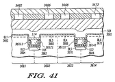
図40は図41に示した実施形態に関して記載した実施形態の回路図を含む。メモリセル3611,3612,3613,3614,3621,3622,3623,3624は、図40に示すようにNVMアレイ18内に配向されている。
Claims (5)
- 電子デバイスであって、
第1の壁と、該第1の壁と対向する第2の壁とを有する、基板内のトレンチと、
第1の方向に実質的に沿って配向された第1のメモリセルのセットと、
前記第1の方向に実質的に沿って配向された第2のメモリセルのセットと、
前記第1のメモリセルのセットに電気的に接続された選択ゲート線である第1のゲート線であって、前記第1のゲート線の少なくとも一部が前記トレンチの外側に存在する、第1のゲート線と、
前記第2のメモリセルのセットに電気的に接続された制御ゲート線である第2のゲート線であって、前記第1のゲート線に比べて第2のゲート線は、前記第1の方向に沿って存在する、より多くのメモリセルのセットに電気的に接続されているとともに、前記第1及び第2のメモリセルのセットを含むメモリアレイ内で前記第1のゲート線が第2のゲート線に実質的に平行であり、前記第2のゲート線の少なくとも一部が前記トレンチ内部に存在する、第2のゲート線と、
複数の不連続記憶素子であって、前記第1のメモリセルのセット内の各メモリセルにおいて、前記複数の不連続記憶素子のうちの第1のセットが、前記トレンチ内部に存在する前記第2のゲート線の少なくとも一部と前記トレンチの前記第1の壁との間に該第1の壁に沿って存在しており、前記第2のメモリセルのセット内の各メモリセルにおいて、前記複数の不連続記憶素子のうちの第2のセットが、前記トレンチ内部に存在する前記第2のゲート線の少なくとも一部と前記トレンチの前記第2の壁との間に該第2の壁に沿って存在している、複数の不連続記憶素子と、
を備える電子デバイス。 - 前記第1および第2のメモリセルのセット内の各メモリセルは、選択ゲート電極および制御ゲート電極を含む不揮発性メモリセルからなり、
前記第1のゲート線は、前記第1のメモリセルのセットの前記選択ゲート電極に電気的に接続されており、
前記第2のゲート線は、前記第2のメモリセルのセットの前記制御ゲート電極に電気的に接続されている、請求項1に記載の電子デバイス。 - 電子デバイスであって、
第1の壁と、該第1の壁と対向する第2の壁とを有する、基板内のトレンチと、
第1の方向に実質的に沿って配向された第1のメモリセルのセットと、
前記第1の方向に実質的に沿って配向された第2のメモリセルのセットと、ここで、前記第1および第2のメモリセルのセット内の各メモリセルは、制御ゲート電極を含み、
前記第1のメモリセルのセットに電気的に接続された第1のビット線であって、他の2つのビット線の間に存在する第1のビット線と、
前記第2のメモリセルのセットに電気的に接続された第2のビット線であって、前記第1のビット線に比べて第2のビット線は、前記第1の方向に沿った、より多くのメモリセルのセットに電気的に接続されているとともに、前記第1及び第2のメモリセルのセットを含むメモリアレイ内で前記第1のビット線が第2のビット線に実質的に平行である、第2のビット線と、
複数の不連続記憶素子であって、前記第1のメモリセルのセット内の各メモリセルにおいて、前記複数の不連続記憶素子のうちの第1のセットが、前記制御ゲート電極と前記トレンチの前記第1の壁との間に該第1の壁に沿って存在しており、前記第2のメモリセルのセット内の各メモリセルにおいて、前記複数の不連続記憶素子のうちの第2のセットが、前記制御ゲート電極と前記トレンチの前記第2の壁との間に該第2の壁に沿って存在している、複数の不連続記憶素子と、
を備える電子デバイス。 - 前記第1および第2のメモリセルのセット内の各メモリセルは、選択ゲート電極および前記制御ゲート電極を含む不揮発性メモリセルからなる、請求項3に記載の電子デバイス。
- 前記第1および第2のメモリセルのセットのチャネル領域と前記制御ゲート電極との間に前記不連続記憶素子が存在し、
前記第1および第2のメモリセルのセットのチャネル領域と前記選択ゲート電極との間には前記不連続記憶素子が実質的に存在しない、請求項4に記載の電子デバイス。
Applications Claiming Priority (3)
| Application Number | Priority Date | Filing Date | Title |
|---|---|---|---|
| US11/188,588 US7642594B2 (en) | 2005-07-25 | 2005-07-25 | Electronic device including gate lines, bit lines, or a combination thereof |
| US11/188,588 | 2005-07-25 | ||
| PCT/US2006/028578 WO2007014117A2 (en) | 2005-07-25 | 2006-07-24 | Non-volatile memory |
Publications (3)
| Publication Number | Publication Date |
|---|---|
| JP2009503859A JP2009503859A (ja) | 2009-01-29 |
| JP2009503859A5 JP2009503859A5 (ja) | 2009-09-10 |
| JP5249757B2 true JP5249757B2 (ja) | 2013-07-31 |
Family
ID=37678281
Family Applications (1)
| Application Number | Title | Priority Date | Filing Date |
|---|---|---|---|
| JP2008524015A Active JP5249757B2 (ja) | 2005-07-25 | 2006-07-24 | 不揮発性メモリ |
Country Status (4)
| Country | Link |
|---|---|
| US (1) | US7642594B2 (ja) |
| JP (1) | JP5249757B2 (ja) |
| TW (1) | TWI404172B (ja) |
| WO (1) | WO2007014117A2 (ja) |
Families Citing this family (13)
| Publication number | Priority date | Publication date | Assignee | Title |
|---|---|---|---|---|
| US7262997B2 (en) * | 2005-07-25 | 2007-08-28 | Freescale Semiconductor, Inc. | Process for operating an electronic device including a memory array and conductive lines |
| US7394686B2 (en) * | 2005-07-25 | 2008-07-01 | Freescale Semiconductor, Inc. | Programmable structure including discontinuous storage elements and spacer control gates in a trench |
| US7667260B2 (en) * | 2006-08-09 | 2010-02-23 | Micron Technology, Inc. | Nanoscale floating gate and methods of formation |
| TW200818402A (en) * | 2006-10-03 | 2008-04-16 | Powerchip Semiconductor Corp | Non-volatile memory, fabricating method and operating method thereof |
| US7651916B2 (en) | 2007-01-24 | 2010-01-26 | Freescale Semiconductor, Inc | Electronic device including trenches and discontinuous storage elements and processes of forming and using the same |
| JP5112731B2 (ja) * | 2007-04-04 | 2013-01-09 | ローム株式会社 | Flotox型eeprom |
| US20120181600A1 (en) * | 2007-08-17 | 2012-07-19 | Masahiko Higashi | Sonos flash memory device |
| JP2010050208A (ja) * | 2008-08-20 | 2010-03-04 | Renesas Technology Corp | 半導体記憶装置 |
| US8999828B2 (en) * | 2011-08-03 | 2015-04-07 | Globalfoundries Singapore Pte. Ltd. | Method and device for a split-gate flash memory with an extended word gate below a channel region |
| US8951892B2 (en) | 2012-06-29 | 2015-02-10 | Freescale Semiconductor, Inc. | Applications for nanopillar structures |
| US9548380B2 (en) | 2013-03-14 | 2017-01-17 | Silicon Storage Technology, Inc. | Non-volatile memory cell having a trapping charge layer in a trench and an array and a method of manufacturing therefor |
| CN106653762B (zh) | 2015-10-30 | 2020-04-21 | 联华电子股份有限公司 | 非挥发性存储器及其制造方法 |
| TWI817325B (zh) * | 2021-11-08 | 2023-10-01 | 南亞科技股份有限公司 | 在多個導電栓塞之間具有矽化物部的半導體元件結構及其製備方法 |
Family Cites Families (100)
| Publication number | Priority date | Publication date | Assignee | Title |
|---|---|---|---|---|
| US4184207A (en) * | 1978-01-27 | 1980-01-15 | Texas Instruments Incorporated | High density floating gate electrically programmable ROM |
| US4751558A (en) * | 1985-10-31 | 1988-06-14 | International Business Machines Corporation | High density memory with field shield |
| US4785337A (en) * | 1986-10-17 | 1988-11-15 | International Business Machines Corporation | Dynamic ram cell having shared trench storage capacitor with sidewall-defined bridge contacts and gate electrodes |
| US4833094A (en) * | 1986-10-17 | 1989-05-23 | International Business Machines Corporation | Method of making a dynamic ram cell having shared trench storage capacitor with sidewall-defined bridge contacts and gate electrodes |
| US4860070A (en) * | 1987-01-09 | 1989-08-22 | Mitsubishi Denki Kabushiki Kaisha | Semiconductor memory device comprising trench memory cells |
| KR910000246B1 (ko) * | 1988-02-15 | 1991-01-23 | 삼성전자 주식회사 | 반도체 메모리장치 |
| US5252845A (en) * | 1990-04-02 | 1993-10-12 | Electronics And Telecommunications Research Institute | Trench DRAM cell with vertical transistor |
| US5196722A (en) * | 1992-03-12 | 1993-03-23 | International Business Machines Corporation | Shadow ram cell having a shallow trench eeprom |
| US5315142A (en) * | 1992-03-23 | 1994-05-24 | International Business Machines Corporation | High performance trench EEPROM cell |
| US5460988A (en) * | 1994-04-25 | 1995-10-24 | United Microelectronics Corporation | Process for high density flash EPROM cell |
| US5411905A (en) * | 1994-04-29 | 1995-05-02 | International Business Machines Corporation | Method of making trench EEPROM structure on SOI with dual channels |
| US5705415A (en) * | 1994-10-04 | 1998-01-06 | Motorola, Inc. | Process for forming an electrically programmable read-only memory cell |
| JP3403877B2 (ja) * | 1995-10-25 | 2003-05-06 | 三菱電機株式会社 | 半導体記憶装置とその製造方法 |
| JPH09129759A (ja) * | 1995-10-31 | 1997-05-16 | Ricoh Co Ltd | 半導体不揮発性メモリ |
| US6110798A (en) * | 1996-01-05 | 2000-08-29 | Micron Technology, Inc. | Method of fabricating an isolation structure on a semiconductor substrate |
| TW326553B (en) * | 1996-01-22 | 1998-02-11 | Handotai Energy Kenkyusho Kk | Semiconductor device and method of fabricating same |
| US5998263A (en) * | 1996-05-16 | 1999-12-07 | Altera Corporation | High-density nonvolatile memory cell |
| US5707897A (en) * | 1996-05-16 | 1998-01-13 | Taiwan Semiconductor Manufacturing Company Ltd. | Non-volatile-memory cell for electrically programmable read only memory having a trench-like coupling capacitors |
| US5824580A (en) * | 1996-07-30 | 1998-10-20 | International Business Machines Corporation | Method of manufacturing an insulated gate field effect transistor |
| US5721448A (en) * | 1996-07-30 | 1998-02-24 | International Business Machines Corporation | Integrated circuit chip having isolation trenches composed of a dielectric layer with oxidation catalyst material |
| JP3320641B2 (ja) * | 1996-09-13 | 2002-09-03 | 株式会社東芝 | メモリセル |
| JP3735426B2 (ja) * | 1996-12-11 | 2006-01-18 | 株式会社東芝 | 不揮発性半導体記憶装置及びその製造方法 |
| US5852306A (en) | 1997-01-29 | 1998-12-22 | Micron Technology, Inc. | Flash memory with nanocrystalline silicon film floating gate |
| US5907775A (en) * | 1997-04-11 | 1999-05-25 | Vanguard International Semiconductor Corporation | Non-volatile memory device with high gate coupling ratio and manufacturing process therefor |
| US6469343B1 (en) | 1998-04-02 | 2002-10-22 | Nippon Steel Corporation | Multi-level type nonvolatile semiconductor memory device |
| US6060743A (en) * | 1997-05-21 | 2000-05-09 | Kabushiki Kaisha Toshiba | Semiconductor memory device having multilayer group IV nanocrystal quantum dot floating gate and method of manufacturing the same |
| US5969383A (en) * | 1997-06-16 | 1999-10-19 | Motorola, Inc. | Split-gate memory device and method for accessing the same |
| JP3211759B2 (ja) * | 1997-12-17 | 2001-09-25 | 日本電気株式会社 | 不揮発性記憶装置の製造方法 |
| US5914523A (en) * | 1998-02-17 | 1999-06-22 | National Semiconductor Corp. | Semiconductor device trench isolation structure with polysilicon bias voltage contact |
| US6087222A (en) * | 1998-03-05 | 2000-07-11 | Taiwan Semiconductor Manufacturing Company | Method of manufacture of vertical split gate flash memory device |
| US6177699B1 (en) * | 1998-03-19 | 2001-01-23 | Lsi Logic Corporation | DRAM cell having a verticle transistor and a capacitor formed on the sidewalls of a trench isolation |
| US6117733A (en) * | 1998-05-27 | 2000-09-12 | Taiwan Semiconductor Manufacturing Company | Poly tip formation and self-align source process for split-gate flash cell |
| US6118147A (en) * | 1998-07-07 | 2000-09-12 | Advanced Micro Devices, Inc. | Double density non-volatile memory cells |
| JP3175700B2 (ja) * | 1998-08-24 | 2001-06-11 | 日本電気株式会社 | メタルゲート電界効果トランジスタの製造方法 |
| US6074954A (en) * | 1998-08-31 | 2000-06-13 | Applied Materials, Inc | Process for control of the shape of the etch front in the etching of polysilicon |
| JP3201370B2 (ja) * | 1999-01-22 | 2001-08-20 | 日本電気株式会社 | 不揮発性半導体記憶装置及びその製造方法 |
| US6433385B1 (en) * | 1999-05-19 | 2002-08-13 | Fairchild Semiconductor Corporation | MOS-gated power device having segmented trench and extended doping zone and process for forming same |
| US6281064B1 (en) * | 1999-06-04 | 2001-08-28 | International Business Machines Corporation | Method for providing dual work function doping and protective insulating cap |
| JP4012341B2 (ja) * | 1999-07-14 | 2007-11-21 | 株式会社ルネサステクノロジ | 半導体集積回路装置 |
| US6255166B1 (en) * | 1999-08-05 | 2001-07-03 | Aalo Lsi Design & Device Technology, Inc. | Nonvolatile memory cell, method of programming the same and nonvolatile memory array |
| US6228706B1 (en) * | 1999-08-26 | 2001-05-08 | International Business Machines Corporation | Vertical DRAM cell with TFT over trench capacitor |
| TW484228B (en) * | 1999-08-31 | 2002-04-21 | Toshiba Corp | Non-volatile semiconductor memory device and the manufacturing method thereof |
| US6287917B1 (en) * | 1999-09-08 | 2001-09-11 | Advanced Micro Devices, Inc. | Process for fabricating an MNOS flash memory device |
| JP3430084B2 (ja) * | 1999-10-22 | 2003-07-28 | 富士通株式会社 | 不揮発性半導体記憶装置の製造方法 |
| US6265268B1 (en) * | 1999-10-25 | 2001-07-24 | Advanced Micro Devices, Inc. | High temperature oxide deposition process for fabricating an ONO floating-gate electrode in a two bit EEPROM device |
| US6172905B1 (en) * | 2000-02-01 | 2001-01-09 | Motorola, Inc. | Method of operating a semiconductor device |
| US6319766B1 (en) * | 2000-02-22 | 2001-11-20 | Applied Materials, Inc. | Method of tantalum nitride deposition by tantalum oxide densification |
| US6320784B1 (en) * | 2000-03-14 | 2001-11-20 | Motorola, Inc. | Memory cell and method for programming thereof |
| US6307782B1 (en) * | 2000-04-03 | 2001-10-23 | Motorola, Inc. | Process for operating a semiconductor device |
| JP4834897B2 (ja) * | 2000-05-02 | 2011-12-14 | ソニー株式会社 | 不揮発性半導体記憶装置およびその動作方法 |
| US6344403B1 (en) * | 2000-06-16 | 2002-02-05 | Motorola, Inc. | Memory device and method for manufacture |
| EP1312120A1 (en) * | 2000-08-14 | 2003-05-21 | Matrix Semiconductor, Inc. | Dense arrays and charge storage devices, and methods for making same |
| US6580124B1 (en) * | 2000-08-14 | 2003-06-17 | Matrix Semiconductor Inc. | Multigate semiconductor device with vertical channel current and method of fabrication |
| US6537870B1 (en) * | 2000-09-29 | 2003-03-25 | Infineon Technologies Ag | Method of forming an integrated circuit comprising a self aligned trench |
| JP4904631B2 (ja) * | 2000-10-27 | 2012-03-28 | ソニー株式会社 | 不揮発性半導体記憶装置およびその製造方法 |
| JP3984020B2 (ja) * | 2000-10-30 | 2007-09-26 | 株式会社東芝 | 不揮発性半導体記憶装置 |
| JP4325972B2 (ja) * | 2001-01-30 | 2009-09-02 | セイコーエプソン株式会社 | 不揮発性半導体記憶装置を含む半導体集積回路装置の製造方法 |
| DE10205345B9 (de) * | 2001-02-09 | 2007-12-20 | Fuji Electric Co., Ltd., Kawasaki | Halbleiterbauelement |
| US6936887B2 (en) * | 2001-05-18 | 2005-08-30 | Sandisk Corporation | Non-volatile memory cells utilizing substrate trenches |
| US6853029B2 (en) * | 2001-05-28 | 2005-02-08 | Kabushiki Kaisha Toshiba | Non-volatile semiconductor memory device with multi-layer gate structure |
| US6762092B2 (en) * | 2001-08-08 | 2004-07-13 | Sandisk Corporation | Scalable self-aligned dual floating gate memory cell array and methods of forming the array |
| JP4665368B2 (ja) * | 2001-09-20 | 2011-04-06 | ソニー株式会社 | 不揮発性半導体メモリ装置、その動作方法および半導体装置の製造方法 |
| KR100400079B1 (ko) * | 2001-10-10 | 2003-09-29 | 한국전자통신연구원 | 트랜치 게이트 구조를 갖는 전력용 반도체 소자의 제조 방법 |
| US6486028B1 (en) * | 2001-11-20 | 2002-11-26 | Macronix International Co., Ltd. | Method of fabricating a nitride read-only-memory cell vertical structure |
| US6747308B2 (en) * | 2001-12-28 | 2004-06-08 | Texas Instruments Incorporated | Single poly EEPROM with reduced area |
| US6818512B1 (en) * | 2002-01-04 | 2004-11-16 | Taiwan Semiconductor Manufacturing Company | Split-gate flash with source/drain multi-sharing |
| US6620664B2 (en) * | 2002-02-07 | 2003-09-16 | Sharp Laboratories Of America, Inc. | Silicon-germanium MOSFET with deposited gate dielectric and metal gate electrode and method for making the same |
| US6461905B1 (en) * | 2002-02-22 | 2002-10-08 | Advanced Micro Devices, Inc. | Dummy gate process to reduce the Vss resistance of flash products |
| US6952034B2 (en) | 2002-04-05 | 2005-10-04 | Silicon Storage Technology, Inc. | Semiconductor memory array of floating gate memory cells with buried source line and floating gate |
| SG125143A1 (en) | 2002-06-21 | 2006-09-29 | Micron Technology Inc | Nrom memory cell, memory array, related devices and methods |
| US6853587B2 (en) * | 2002-06-21 | 2005-02-08 | Micron Technology, Inc. | Vertical NROM having a storage density of 1 bit per 1F2 |
| US6750499B2 (en) * | 2002-08-06 | 2004-06-15 | Intelligent Sources Development Corp. | Self-aligned trench-type dram structure and its contactless dram arrays |
| US6833602B1 (en) | 2002-09-06 | 2004-12-21 | Lattice Semiconductor Corporation | Device having electrically isolated low voltage and high voltage regions and process for fabricating the device |
| TW583755B (en) * | 2002-11-18 | 2004-04-11 | Nanya Technology Corp | Method for fabricating a vertical nitride read-only memory (NROM) cell |
| US7259984B2 (en) * | 2002-11-26 | 2007-08-21 | Cornell Research Foundation, Inc. | Multibit metal nanocrystal memories and fabrication |
| TW569435B (en) * | 2002-12-17 | 2004-01-01 | Nanya Technology Corp | A stacked gate flash memory and the method of fabricating the same |
| US6894339B2 (en) * | 2003-01-02 | 2005-05-17 | Actrans System Inc. | Flash memory with trench select gate and fabrication process |
| JP3985689B2 (ja) * | 2003-02-21 | 2007-10-03 | セイコーエプソン株式会社 | 不揮発性半導体記憶装置 |
| US6706599B1 (en) * | 2003-03-20 | 2004-03-16 | Motorola, Inc. | Multi-bit non-volatile memory device and method therefor |
| US6958513B2 (en) * | 2003-06-06 | 2005-10-25 | Chih-Hsin Wang | Floating-gate memory cell having trench structure with ballistic-charge injector, and the array of memory cells |
| DE10326805B4 (de) * | 2003-06-13 | 2007-02-15 | Infineon Technologies Ag | Herstellungsverfahren für nichtflüchtige Speicherzellen |
| US6818939B1 (en) | 2003-07-18 | 2004-11-16 | Semiconductor Components Industries, L.L.C. | Vertical compound semiconductor field effect transistor structure |
| US6816414B1 (en) * | 2003-07-31 | 2004-11-09 | Freescale Semiconductor, Inc. | Nonvolatile memory and method of making same |
| US6861315B1 (en) * | 2003-08-14 | 2005-03-01 | Silicon Storage Technology, Inc. | Method of manufacturing an array of bi-directional nonvolatile memory cells |
| US7098502B2 (en) * | 2003-11-10 | 2006-08-29 | Freescale Semiconductor, Inc. | Transistor having three electrically isolated electrodes and method of formation |
| US7202523B2 (en) * | 2003-11-17 | 2007-04-10 | Micron Technology, Inc. | NROM flash memory devices on ultrathin silicon |
| US7050330B2 (en) * | 2003-12-16 | 2006-05-23 | Micron Technology, Inc. | Multi-state NROM device |
| US20050148173A1 (en) * | 2004-01-05 | 2005-07-07 | Fuja Shone | Non-volatile memory array having vertical transistors and manufacturing method thereof |
| US6991984B2 (en) * | 2004-01-27 | 2006-01-31 | Freescale Semiconductor, Inc. | Method for forming a memory structure using a modified surface topography and structure thereof |
| US20060113585A1 (en) * | 2004-03-16 | 2006-06-01 | Andy Yu | Non-volatile electrically alterable memory cells for storing multiple data |
| US7015537B2 (en) * | 2004-04-12 | 2006-03-21 | Silicon Storage Technology, Inc. | Isolation-less, contact-less array of nonvolatile memory cells each having a floating gate for storage of charges, and methods of manufacturing, and operating therefor |
| US7629640B2 (en) * | 2004-05-03 | 2009-12-08 | The Regents Of The University Of California | Two bit/four bit SONOS flash memory cell |
| US7196935B2 (en) * | 2004-05-18 | 2007-03-27 | Micron Technolnology, Inc. | Ballistic injection NROM flash memory |
| US6864540B1 (en) * | 2004-05-21 | 2005-03-08 | International Business Machines Corp. | High performance FET with elevated source/drain region |
| US7126188B2 (en) * | 2004-05-27 | 2006-10-24 | Skymedi Corporation | Vertical split gate memory cell and manufacturing method thereof |
| US7262093B2 (en) | 2004-07-15 | 2007-08-28 | Promos Technologies, Inc. | Structure of a non-volatile memory cell and method of forming the same |
| US7199419B2 (en) | 2004-12-13 | 2007-04-03 | Micron Technology, Inc. | Memory structure for reduced floating body effect |
| US7279740B2 (en) * | 2005-05-12 | 2007-10-09 | Micron Technology, Inc. | Band-engineered multi-gated non-volatile memory device with enhanced attributes |
| US7112490B1 (en) * | 2005-07-25 | 2006-09-26 | Freescale Semiconductor, Inc. | Hot carrier injection programmable structure including discontinuous storage elements and spacer control gates in a trench |
| US7592224B2 (en) * | 2006-03-30 | 2009-09-22 | Freescale Semiconductor, Inc | Method of fabricating a storage device including decontinuous storage elements within and between trenches |
-
2005
- 2005-07-25 US US11/188,588 patent/US7642594B2/en not_active Expired - Fee Related
-
2006
- 2006-07-24 WO PCT/US2006/028578 patent/WO2007014117A2/en active Application Filing
- 2006-07-24 JP JP2008524015A patent/JP5249757B2/ja active Active
- 2006-07-25 TW TW095127052A patent/TWI404172B/zh not_active IP Right Cessation
Also Published As
| Publication number | Publication date |
|---|---|
| JP2009503859A (ja) | 2009-01-29 |
| WO2007014117A2 (en) | 2007-02-01 |
| US7642594B2 (en) | 2010-01-05 |
| WO2007014117A3 (en) | 2007-08-30 |
| US20070018234A1 (en) | 2007-01-25 |
| TWI404172B (zh) | 2013-08-01 |
| TW200711050A (en) | 2007-03-16 |
Similar Documents
| Publication | Publication Date | Title |
|---|---|---|
| JP5249757B2 (ja) | 不揮発性メモリ | |
| KR101358693B1 (ko) | 불연속 저장 소자들을 포함하는 전자 디바이스 | |
| US7205608B2 (en) | Electronic device including discontinuous storage elements | |
| US7226840B2 (en) | Process for forming an electronic device including discontinuous storage elements | |
| US7619275B2 (en) | Process for forming an electronic device including discontinuous storage elements | |
| US7211487B2 (en) | Process for forming an electronic device including discontinuous storage elements | |
| US7838922B2 (en) | Electronic device including trenches and discontinuous storage elements | |
| US7256454B2 (en) | Electronic device including discontinuous storage elements and a process for forming the same | |
| JP5781733B2 (ja) | 不揮発性メモリセル及びその製造方法 | |
| US7582929B2 (en) | Electronic device including discontinuous storage elements | |
| US7471560B2 (en) | Electronic device including a memory array and conductive lines | |
| US8193572B2 (en) | Electronic device including trenches and discontinuous storage elements | |
| US7572699B2 (en) | Process of forming an electronic device including fins and discontinuous storage elements | |
| US20130134495A1 (en) | Flash memory and method for forming the same | |
| US20080042191A1 (en) | Non-volatile memory device and method of fabricating the same | |
| TWI396257B (zh) | 包括不連續儲存單元之電子裝置 | |
| JP2008021666A (ja) | 不揮発性半導体記憶装置およびその製造方法 | |
| KR20100078876A (ko) | 플래시 메모리 소자의 제조방법 |
Legal Events
| Date | Code | Title | Description |
|---|---|---|---|
| A521 | Request for written amendment filed |
Free format text: JAPANESE INTERMEDIATE CODE: A523 Effective date: 20090723 |
|
| A621 | Written request for application examination |
Free format text: JAPANESE INTERMEDIATE CODE: A621 Effective date: 20090723 |
|
| A977 | Report on retrieval |
Free format text: JAPANESE INTERMEDIATE CODE: A971007 Effective date: 20120622 |
|
| A131 | Notification of reasons for refusal |
Free format text: JAPANESE INTERMEDIATE CODE: A131 Effective date: 20120703 |
|
| A521 | Request for written amendment filed |
Free format text: JAPANESE INTERMEDIATE CODE: A523 Effective date: 20121003 |
|
| A131 | Notification of reasons for refusal |
Free format text: JAPANESE INTERMEDIATE CODE: A131 Effective date: 20121218 |
|
| A521 | Request for written amendment filed |
Free format text: JAPANESE INTERMEDIATE CODE: A523 Effective date: 20130227 |
|
| TRDD | Decision of grant or rejection written | ||
| A01 | Written decision to grant a patent or to grant a registration (utility model) |
Free format text: JAPANESE INTERMEDIATE CODE: A01 Effective date: 20130319 |
|
| A61 | First payment of annual fees (during grant procedure) |
Free format text: JAPANESE INTERMEDIATE CODE: A61 Effective date: 20130412 |
|
| R150 | Certificate of patent or registration of utility model |
Ref document number: 5249757 Country of ref document: JP Free format text: JAPANESE INTERMEDIATE CODE: R150 Free format text: JAPANESE INTERMEDIATE CODE: R150 |
|
| FPAY | Renewal fee payment (event date is renewal date of database) |
Free format text: PAYMENT UNTIL: 20160419 Year of fee payment: 3 |
|
| R250 | Receipt of annual fees |
Free format text: JAPANESE INTERMEDIATE CODE: R250 |
|
| R250 | Receipt of annual fees |
Free format text: JAPANESE INTERMEDIATE CODE: R250 |
|
| S533 | Written request for registration of change of name |
Free format text: JAPANESE INTERMEDIATE CODE: R313533 |
|
| R350 | Written notification of registration of transfer |
Free format text: JAPANESE INTERMEDIATE CODE: R350 |
|
| R250 | Receipt of annual fees |
Free format text: JAPANESE INTERMEDIATE CODE: R250 |
|
| R250 | Receipt of annual fees |
Free format text: JAPANESE INTERMEDIATE CODE: R250 |
|
| R250 | Receipt of annual fees |
Free format text: JAPANESE INTERMEDIATE CODE: R250 |


