JP5249080B2 - 半導体装置 - Google Patents
半導体装置 Download PDFInfo
- Publication number
- JP5249080B2 JP5249080B2 JP2009036590A JP2009036590A JP5249080B2 JP 5249080 B2 JP5249080 B2 JP 5249080B2 JP 2009036590 A JP2009036590 A JP 2009036590A JP 2009036590 A JP2009036590 A JP 2009036590A JP 5249080 B2 JP5249080 B2 JP 5249080B2
- Authority
- JP
- Japan
- Prior art keywords
- metal wiring
- via hole
- buffer layer
- stress buffer
- metal
- Prior art date
- Legal status (The legal status is an assumption and is not a legal conclusion. Google has not performed a legal analysis and makes no representation as to the accuracy of the status listed.)
- Active
Links
Images


Classifications
-
- H—ELECTRICITY
- H01—ELECTRIC ELEMENTS
- H01L—SEMICONDUCTOR DEVICES NOT COVERED BY CLASS H10
- H01L24/00—Arrangements for connecting or disconnecting semiconductor or solid-state bodies; Methods or apparatus related thereto
- H01L24/01—Means for bonding being attached to, or being formed on, the surface to be connected, e.g. chip-to-package, die-attach, "first-level" interconnects; Manufacturing methods related thereto
- H01L24/02—Bonding areas ; Manufacturing methods related thereto
- H01L24/04—Structure, shape, material or disposition of the bonding areas prior to the connecting process
- H01L24/05—Structure, shape, material or disposition of the bonding areas prior to the connecting process of an individual bonding area
-
- H—ELECTRICITY
- H01—ELECTRIC ELEMENTS
- H01L—SEMICONDUCTOR DEVICES NOT COVERED BY CLASS H10
- H01L24/00—Arrangements for connecting or disconnecting semiconductor or solid-state bodies; Methods or apparatus related thereto
- H01L24/01—Means for bonding being attached to, or being formed on, the surface to be connected, e.g. chip-to-package, die-attach, "first-level" interconnects; Manufacturing methods related thereto
- H01L24/10—Bump connectors ; Manufacturing methods related thereto
- H01L24/12—Structure, shape, material or disposition of the bump connectors prior to the connecting process
-
- H—ELECTRICITY
- H01—ELECTRIC ELEMENTS
- H01L—SEMICONDUCTOR DEVICES NOT COVERED BY CLASS H10
- H01L21/00—Processes or apparatus adapted for the manufacture or treatment of semiconductor or solid state devices or of parts thereof
- H01L21/02—Manufacture or treatment of semiconductor devices or of parts thereof
- H01L21/02104—Forming layers
- H01L21/02107—Forming insulating materials on a substrate
- H01L21/02109—Forming insulating materials on a substrate characterised by the type of layer, e.g. type of material, porous/non-porous, pre-cursors, mixtures or laminates
- H01L21/02112—Forming insulating materials on a substrate characterised by the type of layer, e.g. type of material, porous/non-porous, pre-cursors, mixtures or laminates characterised by the material of the layer
-
- H—ELECTRICITY
- H01—ELECTRIC ELEMENTS
- H01L—SEMICONDUCTOR DEVICES NOT COVERED BY CLASS H10
- H01L24/00—Arrangements for connecting or disconnecting semiconductor or solid-state bodies; Methods or apparatus related thereto
- H01L24/01—Means for bonding being attached to, or being formed on, the surface to be connected, e.g. chip-to-package, die-attach, "first-level" interconnects; Manufacturing methods related thereto
- H01L24/10—Bump connectors ; Manufacturing methods related thereto
- H01L24/12—Structure, shape, material or disposition of the bump connectors prior to the connecting process
- H01L24/13—Structure, shape, material or disposition of the bump connectors prior to the connecting process of an individual bump connector
-
- H—ELECTRICITY
- H01—ELECTRIC ELEMENTS
- H01L—SEMICONDUCTOR DEVICES NOT COVERED BY CLASS H10
- H01L2224/00—Indexing scheme for arrangements for connecting or disconnecting semiconductor or solid-state bodies and methods related thereto as covered by H01L24/00
- H01L2224/01—Means for bonding being attached to, or being formed on, the surface to be connected, e.g. chip-to-package, die-attach, "first-level" interconnects; Manufacturing methods related thereto
- H01L2224/02—Bonding areas; Manufacturing methods related thereto
- H01L2224/023—Redistribution layers [RDL] for bonding areas
-
- H—ELECTRICITY
- H01—ELECTRIC ELEMENTS
- H01L—SEMICONDUCTOR DEVICES NOT COVERED BY CLASS H10
- H01L2224/00—Indexing scheme for arrangements for connecting or disconnecting semiconductor or solid-state bodies and methods related thereto as covered by H01L24/00
- H01L2224/01—Means for bonding being attached to, or being formed on, the surface to be connected, e.g. chip-to-package, die-attach, "first-level" interconnects; Manufacturing methods related thereto
- H01L2224/02—Bonding areas; Manufacturing methods related thereto
- H01L2224/04—Structure, shape, material or disposition of the bonding areas prior to the connecting process
- H01L2224/0401—Bonding areas specifically adapted for bump connectors, e.g. under bump metallisation [UBM]
-
- H—ELECTRICITY
- H01—ELECTRIC ELEMENTS
- H01L—SEMICONDUCTOR DEVICES NOT COVERED BY CLASS H10
- H01L2224/00—Indexing scheme for arrangements for connecting or disconnecting semiconductor or solid-state bodies and methods related thereto as covered by H01L24/00
- H01L2224/01—Means for bonding being attached to, or being formed on, the surface to be connected, e.g. chip-to-package, die-attach, "first-level" interconnects; Manufacturing methods related thereto
- H01L2224/02—Bonding areas; Manufacturing methods related thereto
- H01L2224/04—Structure, shape, material or disposition of the bonding areas prior to the connecting process
- H01L2224/05—Structure, shape, material or disposition of the bonding areas prior to the connecting process of an individual bonding area
- H01L2224/05001—Internal layers
- H01L2224/05099—Material
- H01L2224/051—Material with a principal constituent of the material being a metal or a metalloid, e.g. boron [B], silicon [Si], germanium [Ge], arsenic [As], antimony [Sb], tellurium [Te] and polonium [Po], and alloys thereof
- H01L2224/05117—Material with a principal constituent of the material being a metal or a metalloid, e.g. boron [B], silicon [Si], germanium [Ge], arsenic [As], antimony [Sb], tellurium [Te] and polonium [Po], and alloys thereof the principal constituent melting at a temperature of greater than or equal to 400°C and less than 950°C
- H01L2224/05124—Aluminium [Al] as principal constituent
-
- H—ELECTRICITY
- H01—ELECTRIC ELEMENTS
- H01L—SEMICONDUCTOR DEVICES NOT COVERED BY CLASS H10
- H01L2224/00—Indexing scheme for arrangements for connecting or disconnecting semiconductor or solid-state bodies and methods related thereto as covered by H01L24/00
- H01L2224/01—Means for bonding being attached to, or being formed on, the surface to be connected, e.g. chip-to-package, die-attach, "first-level" interconnects; Manufacturing methods related thereto
- H01L2224/02—Bonding areas; Manufacturing methods related thereto
- H01L2224/04—Structure, shape, material or disposition of the bonding areas prior to the connecting process
- H01L2224/05—Structure, shape, material or disposition of the bonding areas prior to the connecting process of an individual bonding area
- H01L2224/05001—Internal layers
- H01L2224/05099—Material
- H01L2224/051—Material with a principal constituent of the material being a metal or a metalloid, e.g. boron [B], silicon [Si], germanium [Ge], arsenic [As], antimony [Sb], tellurium [Te] and polonium [Po], and alloys thereof
- H01L2224/05138—Material with a principal constituent of the material being a metal or a metalloid, e.g. boron [B], silicon [Si], germanium [Ge], arsenic [As], antimony [Sb], tellurium [Te] and polonium [Po], and alloys thereof the principal constituent melting at a temperature of greater than or equal to 950°C and less than 1550°C
- H01L2224/05147—Copper [Cu] as principal constituent
-
- H—ELECTRICITY
- H01—ELECTRIC ELEMENTS
- H01L—SEMICONDUCTOR DEVICES NOT COVERED BY CLASS H10
- H01L2224/00—Indexing scheme for arrangements for connecting or disconnecting semiconductor or solid-state bodies and methods related thereto as covered by H01L24/00
- H01L2224/01—Means for bonding being attached to, or being formed on, the surface to be connected, e.g. chip-to-package, die-attach, "first-level" interconnects; Manufacturing methods related thereto
- H01L2224/02—Bonding areas; Manufacturing methods related thereto
- H01L2224/04—Structure, shape, material or disposition of the bonding areas prior to the connecting process
- H01L2224/05—Structure, shape, material or disposition of the bonding areas prior to the connecting process of an individual bonding area
- H01L2224/05001—Internal layers
- H01L2224/05099—Material
- H01L2224/051—Material with a principal constituent of the material being a metal or a metalloid, e.g. boron [B], silicon [Si], germanium [Ge], arsenic [As], antimony [Sb], tellurium [Te] and polonium [Po], and alloys thereof
- H01L2224/05163—Material with a principal constituent of the material being a metal or a metalloid, e.g. boron [B], silicon [Si], germanium [Ge], arsenic [As], antimony [Sb], tellurium [Te] and polonium [Po], and alloys thereof the principal constituent melting at a temperature of greater than 1550°C
- H01L2224/05166—Titanium [Ti] as principal constituent
-
- H—ELECTRICITY
- H01—ELECTRIC ELEMENTS
- H01L—SEMICONDUCTOR DEVICES NOT COVERED BY CLASS H10
- H01L2224/00—Indexing scheme for arrangements for connecting or disconnecting semiconductor or solid-state bodies and methods related thereto as covered by H01L24/00
- H01L2224/01—Means for bonding being attached to, or being formed on, the surface to be connected, e.g. chip-to-package, die-attach, "first-level" interconnects; Manufacturing methods related thereto
- H01L2224/02—Bonding areas; Manufacturing methods related thereto
- H01L2224/04—Structure, shape, material or disposition of the bonding areas prior to the connecting process
- H01L2224/05—Structure, shape, material or disposition of the bonding areas prior to the connecting process of an individual bonding area
- H01L2224/0554—External layer
- H01L2224/0555—Shape
- H01L2224/05556—Shape in side view
- H01L2224/05559—Shape in side view non conformal layer on a patterned surface
-
- H—ELECTRICITY
- H01—ELECTRIC ELEMENTS
- H01L—SEMICONDUCTOR DEVICES NOT COVERED BY CLASS H10
- H01L2224/00—Indexing scheme for arrangements for connecting or disconnecting semiconductor or solid-state bodies and methods related thereto as covered by H01L24/00
- H01L2224/01—Means for bonding being attached to, or being formed on, the surface to be connected, e.g. chip-to-package, die-attach, "first-level" interconnects; Manufacturing methods related thereto
- H01L2224/02—Bonding areas; Manufacturing methods related thereto
- H01L2224/04—Structure, shape, material or disposition of the bonding areas prior to the connecting process
- H01L2224/05—Structure, shape, material or disposition of the bonding areas prior to the connecting process of an individual bonding area
- H01L2224/0554—External layer
- H01L2224/0556—Disposition
- H01L2224/05571—Disposition the external layer being disposed in a recess of the surface
- H01L2224/05572—Disposition the external layer being disposed in a recess of the surface the external layer extending out of an opening
-
- H—ELECTRICITY
- H01—ELECTRIC ELEMENTS
- H01L—SEMICONDUCTOR DEVICES NOT COVERED BY CLASS H10
- H01L2224/00—Indexing scheme for arrangements for connecting or disconnecting semiconductor or solid-state bodies and methods related thereto as covered by H01L24/00
- H01L2224/01—Means for bonding being attached to, or being formed on, the surface to be connected, e.g. chip-to-package, die-attach, "first-level" interconnects; Manufacturing methods related thereto
- H01L2224/02—Bonding areas; Manufacturing methods related thereto
- H01L2224/04—Structure, shape, material or disposition of the bonding areas prior to the connecting process
- H01L2224/05—Structure, shape, material or disposition of the bonding areas prior to the connecting process of an individual bonding area
- H01L2224/0554—External layer
- H01L2224/05599—Material
- H01L2224/056—Material with a principal constituent of the material being a metal or a metalloid, e.g. boron [B], silicon [Si], germanium [Ge], arsenic [As], antimony [Sb], tellurium [Te] and polonium [Po], and alloys thereof
- H01L2224/05638—Material with a principal constituent of the material being a metal or a metalloid, e.g. boron [B], silicon [Si], germanium [Ge], arsenic [As], antimony [Sb], tellurium [Te] and polonium [Po], and alloys thereof the principal constituent melting at a temperature of greater than or equal to 950°C and less than 1550°C
- H01L2224/05647—Copper [Cu] as principal constituent
-
- H—ELECTRICITY
- H01—ELECTRIC ELEMENTS
- H01L—SEMICONDUCTOR DEVICES NOT COVERED BY CLASS H10
- H01L2224/00—Indexing scheme for arrangements for connecting or disconnecting semiconductor or solid-state bodies and methods related thereto as covered by H01L24/00
- H01L2224/01—Means for bonding being attached to, or being formed on, the surface to be connected, e.g. chip-to-package, die-attach, "first-level" interconnects; Manufacturing methods related thereto
- H01L2224/10—Bump connectors; Manufacturing methods related thereto
- H01L2224/12—Structure, shape, material or disposition of the bump connectors prior to the connecting process
- H01L2224/13—Structure, shape, material or disposition of the bump connectors prior to the connecting process of an individual bump connector
- H01L2224/13001—Core members of the bump connector
- H01L2224/1302—Disposition
- H01L2224/13021—Disposition the bump connector being disposed in a recess of the surface
-
- H—ELECTRICITY
- H01—ELECTRIC ELEMENTS
- H01L—SEMICONDUCTOR DEVICES NOT COVERED BY CLASS H10
- H01L2224/00—Indexing scheme for arrangements for connecting or disconnecting semiconductor or solid-state bodies and methods related thereto as covered by H01L24/00
- H01L2224/01—Means for bonding being attached to, or being formed on, the surface to be connected, e.g. chip-to-package, die-attach, "first-level" interconnects; Manufacturing methods related thereto
- H01L2224/10—Bump connectors; Manufacturing methods related thereto
- H01L2224/12—Structure, shape, material or disposition of the bump connectors prior to the connecting process
- H01L2224/13—Structure, shape, material or disposition of the bump connectors prior to the connecting process of an individual bump connector
- H01L2224/13001—Core members of the bump connector
- H01L2224/1302—Disposition
- H01L2224/13026—Disposition relative to the bonding area, e.g. bond pad, of the semiconductor or solid-state body
- H01L2224/13027—Disposition relative to the bonding area, e.g. bond pad, of the semiconductor or solid-state body the bump connector being offset with respect to the bonding area, e.g. bond pad
-
- H—ELECTRICITY
- H01—ELECTRIC ELEMENTS
- H01L—SEMICONDUCTOR DEVICES NOT COVERED BY CLASS H10
- H01L2224/00—Indexing scheme for arrangements for connecting or disconnecting semiconductor or solid-state bodies and methods related thereto as covered by H01L24/00
- H01L2224/01—Means for bonding being attached to, or being formed on, the surface to be connected, e.g. chip-to-package, die-attach, "first-level" interconnects; Manufacturing methods related thereto
- H01L2224/10—Bump connectors; Manufacturing methods related thereto
- H01L2224/12—Structure, shape, material or disposition of the bump connectors prior to the connecting process
- H01L2224/13—Structure, shape, material or disposition of the bump connectors prior to the connecting process of an individual bump connector
- H01L2224/13001—Core members of the bump connector
- H01L2224/13099—Material
-
- H—ELECTRICITY
- H01—ELECTRIC ELEMENTS
- H01L—SEMICONDUCTOR DEVICES NOT COVERED BY CLASS H10
- H01L2224/00—Indexing scheme for arrangements for connecting or disconnecting semiconductor or solid-state bodies and methods related thereto as covered by H01L24/00
- H01L2224/01—Means for bonding being attached to, or being formed on, the surface to be connected, e.g. chip-to-package, die-attach, "first-level" interconnects; Manufacturing methods related thereto
- H01L2224/10—Bump connectors; Manufacturing methods related thereto
- H01L2224/15—Structure, shape, material or disposition of the bump connectors after the connecting process
- H01L2224/16—Structure, shape, material or disposition of the bump connectors after the connecting process of an individual bump connector
-
- H—ELECTRICITY
- H01—ELECTRIC ELEMENTS
- H01L—SEMICONDUCTOR DEVICES NOT COVERED BY CLASS H10
- H01L24/00—Arrangements for connecting or disconnecting semiconductor or solid-state bodies; Methods or apparatus related thereto
- H01L24/01—Means for bonding being attached to, or being formed on, the surface to be connected, e.g. chip-to-package, die-attach, "first-level" interconnects; Manufacturing methods related thereto
- H01L24/02—Bonding areas ; Manufacturing methods related thereto
- H01L24/03—Manufacturing methods
-
- H—ELECTRICITY
- H01—ELECTRIC ELEMENTS
- H01L—SEMICONDUCTOR DEVICES NOT COVERED BY CLASS H10
- H01L2924/00—Indexing scheme for arrangements or methods for connecting or disconnecting semiconductor or solid-state bodies as covered by H01L24/00
- H01L2924/0001—Technical content checked by a classifier
- H01L2924/0002—Not covered by any one of groups H01L24/00, H01L24/00 and H01L2224/00
-
- H—ELECTRICITY
- H01—ELECTRIC ELEMENTS
- H01L—SEMICONDUCTOR DEVICES NOT COVERED BY CLASS H10
- H01L2924/00—Indexing scheme for arrangements or methods for connecting or disconnecting semiconductor or solid-state bodies as covered by H01L24/00
- H01L2924/01—Chemical elements
- H01L2924/01006—Carbon [C]
-
- H—ELECTRICITY
- H01—ELECTRIC ELEMENTS
- H01L—SEMICONDUCTOR DEVICES NOT COVERED BY CLASS H10
- H01L2924/00—Indexing scheme for arrangements or methods for connecting or disconnecting semiconductor or solid-state bodies as covered by H01L24/00
- H01L2924/01—Chemical elements
- H01L2924/01013—Aluminum [Al]
-
- H—ELECTRICITY
- H01—ELECTRIC ELEMENTS
- H01L—SEMICONDUCTOR DEVICES NOT COVERED BY CLASS H10
- H01L2924/00—Indexing scheme for arrangements or methods for connecting or disconnecting semiconductor or solid-state bodies as covered by H01L24/00
- H01L2924/01—Chemical elements
- H01L2924/01015—Phosphorus [P]
-
- H—ELECTRICITY
- H01—ELECTRIC ELEMENTS
- H01L—SEMICONDUCTOR DEVICES NOT COVERED BY CLASS H10
- H01L2924/00—Indexing scheme for arrangements or methods for connecting or disconnecting semiconductor or solid-state bodies as covered by H01L24/00
- H01L2924/01—Chemical elements
- H01L2924/01016—Sulfur [S]
-
- H—ELECTRICITY
- H01—ELECTRIC ELEMENTS
- H01L—SEMICONDUCTOR DEVICES NOT COVERED BY CLASS H10
- H01L2924/00—Indexing scheme for arrangements or methods for connecting or disconnecting semiconductor or solid-state bodies as covered by H01L24/00
- H01L2924/01—Chemical elements
- H01L2924/01022—Titanium [Ti]
-
- H—ELECTRICITY
- H01—ELECTRIC ELEMENTS
- H01L—SEMICONDUCTOR DEVICES NOT COVERED BY CLASS H10
- H01L2924/00—Indexing scheme for arrangements or methods for connecting or disconnecting semiconductor or solid-state bodies as covered by H01L24/00
- H01L2924/01—Chemical elements
- H01L2924/01024—Chromium [Cr]
-
- H—ELECTRICITY
- H01—ELECTRIC ELEMENTS
- H01L—SEMICONDUCTOR DEVICES NOT COVERED BY CLASS H10
- H01L2924/00—Indexing scheme for arrangements or methods for connecting or disconnecting semiconductor or solid-state bodies as covered by H01L24/00
- H01L2924/01—Chemical elements
- H01L2924/01029—Copper [Cu]
-
- H—ELECTRICITY
- H01—ELECTRIC ELEMENTS
- H01L—SEMICONDUCTOR DEVICES NOT COVERED BY CLASS H10
- H01L2924/00—Indexing scheme for arrangements or methods for connecting or disconnecting semiconductor or solid-state bodies as covered by H01L24/00
- H01L2924/01—Chemical elements
- H01L2924/01033—Arsenic [As]
-
- H—ELECTRICITY
- H01—ELECTRIC ELEMENTS
- H01L—SEMICONDUCTOR DEVICES NOT COVERED BY CLASS H10
- H01L2924/00—Indexing scheme for arrangements or methods for connecting or disconnecting semiconductor or solid-state bodies as covered by H01L24/00
- H01L2924/01—Chemical elements
- H01L2924/01074—Tungsten [W]
-
- H—ELECTRICITY
- H01—ELECTRIC ELEMENTS
- H01L—SEMICONDUCTOR DEVICES NOT COVERED BY CLASS H10
- H01L2924/00—Indexing scheme for arrangements or methods for connecting or disconnecting semiconductor or solid-state bodies as covered by H01L24/00
- H01L2924/01—Chemical elements
- H01L2924/01078—Platinum [Pt]
-
- H—ELECTRICITY
- H01—ELECTRIC ELEMENTS
- H01L—SEMICONDUCTOR DEVICES NOT COVERED BY CLASS H10
- H01L2924/00—Indexing scheme for arrangements or methods for connecting or disconnecting semiconductor or solid-state bodies as covered by H01L24/00
- H01L2924/01—Chemical elements
- H01L2924/01079—Gold [Au]
-
- H—ELECTRICITY
- H01—ELECTRIC ELEMENTS
- H01L—SEMICONDUCTOR DEVICES NOT COVERED BY CLASS H10
- H01L2924/00—Indexing scheme for arrangements or methods for connecting or disconnecting semiconductor or solid-state bodies as covered by H01L24/00
- H01L2924/013—Alloys
- H01L2924/014—Solder alloys
Description
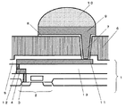
2 半導体素子
3 金属配線
4 入出力の金属端子
5 保護膜
6 応力緩衝層
7 ビアホール
8 下地金属
9 導電層
10 バンプ電極
11 再配線(第2の金属配線)
12 金属配線のビア
13 絶縁膜
21 第1の応力緩衝層
22 第2の応力緩衝層
23 第1の開口孔
24 第2の開口孔
25 再配線(第1の応力緩衝層の上の導電層)
26 バンプ電極(スクリーニング印刷)
Claims (2)
- 半導体基板と、
前記半導体基板に設けられた半導体素子上に配置された金属配線と、
前記金属配線の上に形成され、前記金属配線を保護する保護膜と、
前記保護膜の上に形成された、セラミック膜と前記セラミック膜より機械的剛性の小さい材料の2層からなる応力緩衝層と、
前記保護膜及び、前記応力緩衝層を貫通して、前記金属配線上に設けられたビアホールと、
前記ビアホールの内面及び前記金属配線の表面、及び前記応力緩衝層の表面に形成された下地金属膜と、
前記ビアホールを埋め込むように形成された導電層と、
前記導電層の上に形成されたバンプ電極を有し、
平面視にて、前記ビアホールは前記バンプ電極の中心を避けて、前記バンプ電極の下ではあるが周囲の領域に形成されていることを特徴とする半導体装置。 - 半導体基板と、
前記半導体基板に設けられた半導体素子上に配置された第1の金属配線と、
前記第1の金属配線の上に絶縁膜を介して配置された第2の金属配線と、
前記第2の金属配線の上に形成され、前記金属配線を保護する保護膜と、
前記保護膜の上に形成された、セラミック膜と前記セラミック膜より機械的剛性の小さい材料の2層からなる応力緩衝層と、
前記保護膜及び、前記応力緩衝層を貫通して、前記第2の金属配線上に設けられたビアホールと、
前記ビアホールの内面及び前記第2の金属配線の表面、及び前記応力緩衝層の表面に形成された下地金属膜と、
前記ビアホールを埋め込むように形成された導電層と、
前記導電層の上に形成されたバンプ電極と、
前記半導体素子上に前記第1の金属配線により形成された入出力のための金属端子と、を有し、
前記第2の金属配線は前記バンプ電極及び前記ビアホール内に形成された前記導電層と前記金属端子とを、前記金属端子上に設けられたビアを介してつなぐ再配線であり、
平面視にて、前記ビアホールは前記バンプ電極の中心を避けて、前記バンプ電極の下で
はあるが周囲の領域に形成されていることを特徴とする半導体装置。
Priority Applications (5)
| Application Number | Priority Date | Filing Date | Title |
|---|---|---|---|
| JP2009036590A JP5249080B2 (ja) | 2009-02-19 | 2009-02-19 | 半導体装置 |
| TW099103347A TWI501364B (zh) | 2009-02-19 | 2010-02-04 | 半導體裝置 |
| CN201010117406.XA CN101814476B (zh) | 2009-02-19 | 2010-02-12 | 半导体装置 |
| KR1020100013796A KR20100094943A (ko) | 2009-02-19 | 2010-02-16 | 반도체 장치 |
| US12/707,348 US20100207271A1 (en) | 2009-02-19 | 2010-02-17 | Semiconductor device |
Applications Claiming Priority (1)
| Application Number | Priority Date | Filing Date | Title |
|---|---|---|---|
| JP2009036590A JP5249080B2 (ja) | 2009-02-19 | 2009-02-19 | 半導体装置 |
Publications (3)
| Publication Number | Publication Date |
|---|---|
| JP2010192747A JP2010192747A (ja) | 2010-09-02 |
| JP2010192747A5 JP2010192747A5 (ja) | 2012-01-26 |
| JP5249080B2 true JP5249080B2 (ja) | 2013-07-31 |
Family
ID=42559187
Family Applications (1)
| Application Number | Title | Priority Date | Filing Date |
|---|---|---|---|
| JP2009036590A Active JP5249080B2 (ja) | 2009-02-19 | 2009-02-19 | 半導体装置 |
Country Status (5)
| Country | Link |
|---|---|
| US (1) | US20100207271A1 (ja) |
| JP (1) | JP5249080B2 (ja) |
| KR (1) | KR20100094943A (ja) |
| CN (1) | CN101814476B (ja) |
| TW (1) | TWI501364B (ja) |
Families Citing this family (9)
| Publication number | Priority date | Publication date | Assignee | Title |
|---|---|---|---|---|
| KR102012935B1 (ko) | 2012-06-13 | 2019-08-21 | 삼성전자주식회사 | 전기적 연결 구조 및 그의 제조방법 |
| KR20140041975A (ko) | 2012-09-25 | 2014-04-07 | 삼성전자주식회사 | 범프 구조체 및 이를 포함하는 전기적 연결 구조체 |
| US8772151B2 (en) | 2012-09-27 | 2014-07-08 | Taiwan Semiconductor Manufacturing Company, Ltd. | Passivation scheme |
| KR102122456B1 (ko) | 2013-12-20 | 2020-06-12 | 삼성전자주식회사 | 실리콘 관통 비아 플러그들을 갖는 반도체 소자 및 이를 포함하는 반도체 패키지 |
| KR102212559B1 (ko) | 2014-08-20 | 2021-02-08 | 삼성전자주식회사 | 반도체 발광소자 및 이를 이용한 반도체 발광소자 패키지 |
| JP6565238B2 (ja) * | 2015-03-17 | 2019-08-28 | セイコーエプソン株式会社 | 液体噴射ヘッド |
| CN109309057A (zh) * | 2017-07-26 | 2019-02-05 | 中芯国际集成电路制造(上海)有限公司 | 半导体结构及其形成方法 |
| KR20210084736A (ko) * | 2019-12-27 | 2021-07-08 | 삼성전자주식회사 | 반도체 패키지 |
| KR20210086198A (ko) | 2019-12-31 | 2021-07-08 | 삼성전자주식회사 | 반도체 패키지 |
Family Cites Families (74)
| Publication number | Priority date | Publication date | Assignee | Title |
|---|---|---|---|---|
| US4087314A (en) * | 1976-09-13 | 1978-05-02 | Motorola, Inc. | Bonding pedestals for semiconductor devices |
| JPS60117633A (ja) * | 1983-11-30 | 1985-06-25 | Toshiba Corp | 半導体装置 |
| US5134460A (en) * | 1986-08-11 | 1992-07-28 | International Business Machines Corporation | Aluminum bump, reworkable bump, and titanium nitride structure for tab bonding |
| KR910006967B1 (ko) * | 1987-11-18 | 1991-09-14 | 가시오 게이상기 가부시기가이샤 | 반도체 장치의 범프 전극 구조 및 그 형성 방법 |
| US5719448A (en) * | 1989-03-07 | 1998-02-17 | Seiko Epson Corporation | Bonding pad structures for semiconductor integrated circuits |
| US5027253A (en) * | 1990-04-09 | 1991-06-25 | Ibm Corporation | Printed circuit boards and cards having buried thin film capacitors and processing techniques for fabricating said boards and cards |
| US5136364A (en) * | 1991-06-12 | 1992-08-04 | National Semiconductor Corporation | Semiconductor die sealing |
| JPH06204344A (ja) * | 1992-12-25 | 1994-07-22 | Hitachi Denshi Ltd | 半導体装置の製造方法 |
| JP2596331B2 (ja) * | 1993-09-08 | 1997-04-02 | 日本電気株式会社 | 半導体装置およびその製造方法 |
| JP3217624B2 (ja) * | 1994-11-12 | 2001-10-09 | 東芝マイクロエレクトロニクス株式会社 | 半導体装置 |
| JP3660799B2 (ja) * | 1997-09-08 | 2005-06-15 | 株式会社ルネサステクノロジ | 半導体集積回路装置の製造方法 |
| US5943597A (en) * | 1998-06-15 | 1999-08-24 | Motorola, Inc. | Bumped semiconductor device having a trench for stress relief |
| US6077726A (en) * | 1998-07-30 | 2000-06-20 | Motorola, Inc. | Method and apparatus for stress relief in solder bump formation on a semiconductor device |
| JP3408172B2 (ja) * | 1998-12-10 | 2003-05-19 | 三洋電機株式会社 | チップサイズパッケージ及びその製造方法 |
| US6756295B2 (en) * | 1998-12-21 | 2004-06-29 | Megic Corporation | Chip structure and process for forming the same |
| US8021976B2 (en) * | 2002-10-15 | 2011-09-20 | Megica Corporation | Method of wire bonding over active area of a semiconductor circuit |
| US6479900B1 (en) * | 1998-12-22 | 2002-11-12 | Sanyo Electric Co., Ltd. | Semiconductor device and method of manufacturing the same |
| US6011314A (en) * | 1999-02-01 | 2000-01-04 | Hewlett-Packard Company | Redistribution layer and under bump material structure for converting periphery conductive pads to an array of solder bumps |
| KR100411679B1 (ko) * | 1999-03-16 | 2003-12-18 | 세이코 엡슨 가부시키가이샤 | 반도체 장치 및 그 제조 방법, 회로 기판 및 전자기기 |
| US6133136A (en) * | 1999-05-19 | 2000-10-17 | International Business Machines Corporation | Robust interconnect structure |
| US6387734B1 (en) * | 1999-06-11 | 2002-05-14 | Fujikura Ltd. | Semiconductor package, semiconductor device, electronic device and production method for semiconductor package |
| US6391780B1 (en) * | 1999-08-23 | 2002-05-21 | Taiwan Semiconductor Manufacturing Company | Method to prevent copper CMP dishing |
| JP3387083B2 (ja) * | 1999-08-27 | 2003-03-17 | 日本電気株式会社 | 半導体装置及びその製造方法 |
| US6451681B1 (en) * | 1999-10-04 | 2002-09-17 | Motorola, Inc. | Method of forming copper interconnection utilizing aluminum capping film |
| US6803302B2 (en) * | 1999-11-22 | 2004-10-12 | Freescale Semiconductor, Inc. | Method for forming a semiconductor device having a mechanically robust pad interface |
| JP2001196413A (ja) * | 2000-01-12 | 2001-07-19 | Mitsubishi Electric Corp | 半導体装置、該半導体装置の製造方法、cmp装置、及びcmp方法 |
| US6555908B1 (en) * | 2000-02-10 | 2003-04-29 | Epic Technologies, Inc. | Compliant, solderable input/output bump structures |
| JP3651765B2 (ja) * | 2000-03-27 | 2005-05-25 | 株式会社東芝 | 半導体装置 |
| US6300234B1 (en) * | 2000-06-26 | 2001-10-09 | Motorola, Inc. | Process for forming an electrical device |
| US6560862B1 (en) * | 2001-02-06 | 2003-05-13 | Taiwan Semiconductor Manufacturing Company | Modified pad for copper/low-k |
| TW594993B (en) * | 2001-02-16 | 2004-06-21 | Sanyo Electric Co | Semiconductor device and manufacturing process therefor |
| JP2003031576A (ja) * | 2001-07-17 | 2003-01-31 | Nec Corp | 半導体素子及びその製造方法 |
| JP2003031575A (ja) * | 2001-07-17 | 2003-01-31 | Nec Corp | 半導体装置及びその製造方法 |
| US20030116845A1 (en) * | 2001-12-21 | 2003-06-26 | Bojkov Christo P. | Waferlevel method for direct bumping on copper pads in integrated circuits |
| US6844631B2 (en) * | 2002-03-13 | 2005-01-18 | Freescale Semiconductor, Inc. | Semiconductor device having a bond pad and method therefor |
| JP2003318324A (ja) * | 2002-04-26 | 2003-11-07 | Sony Corp | 半導体装置 |
| KR20040061970A (ko) * | 2002-12-31 | 2004-07-07 | 동부전자 주식회사 | 반도체소자의 패드 형성방법 |
| TWI225899B (en) * | 2003-02-18 | 2005-01-01 | Unitive Semiconductor Taiwan C | Etching solution and method for manufacturing conductive bump using the etching solution to selectively remove barrier layer |
| US7244671B2 (en) * | 2003-07-25 | 2007-07-17 | Unitive International Limited | Methods of forming conductive structures including titanium-tungsten base layers and related structures |
| TWI224377B (en) * | 2003-11-14 | 2004-11-21 | Ind Tech Res Inst | Wafer level chip scale packaging structure and method of fabrication the same |
| JP3973624B2 (ja) * | 2003-12-24 | 2007-09-12 | 富士通株式会社 | 高周波デバイス |
| US7176583B2 (en) * | 2004-07-21 | 2007-02-13 | International Business Machines Corporation | Damascene patterning of barrier layer metal for C4 solder bumps |
| DE102004047730B4 (de) * | 2004-09-30 | 2017-06-22 | Advanced Micro Devices, Inc. | Ein Verfahren zum Dünnen von Halbleitersubstraten zur Herstellung von dünnen Halbleiterplättchen |
| WO2006050127A2 (en) * | 2004-10-29 | 2006-05-11 | Flipchip International, Llc | Semiconductor device package with bump overlying a polymer layer |
| US20060128072A1 (en) * | 2004-12-13 | 2006-06-15 | Lsi Logic Corporation | Method of protecting fuses in an integrated circuit die |
| JP4777644B2 (ja) * | 2004-12-24 | 2011-09-21 | Okiセミコンダクタ株式会社 | 半導体装置およびその製造方法 |
| TWI245345B (en) * | 2005-02-17 | 2005-12-11 | Touch Micro System Tech | Method of forming a wear-resistant dielectric layer |
| JP4097660B2 (ja) * | 2005-04-06 | 2008-06-11 | シャープ株式会社 | 半導体装置 |
| US7427565B2 (en) * | 2005-06-30 | 2008-09-23 | Intel Corporation | Multi-step etch for metal bump formation |
| JP2007073681A (ja) * | 2005-09-06 | 2007-03-22 | Renesas Technology Corp | 半導体装置およびその製造方法 |
| US7566650B2 (en) * | 2005-09-23 | 2009-07-28 | Stats Chippac Ltd. | Integrated circuit solder bumping system |
| US7518211B2 (en) * | 2005-11-11 | 2009-04-14 | United Microelectronics Corp. | Chip and package structure |
| US7947978B2 (en) * | 2005-12-05 | 2011-05-24 | Megica Corporation | Semiconductor chip with bond area |
| WO2007074529A1 (ja) * | 2005-12-27 | 2007-07-05 | Fujitsu Limited | 半導体装置 |
| KR100703559B1 (ko) * | 2005-12-28 | 2007-04-03 | 동부일렉트로닉스 주식회사 | 듀얼다마신 구조를 가지는 반도체 소자 및 그 제조방법 |
| KR100870820B1 (ko) * | 2005-12-29 | 2008-11-27 | 매그나칩 반도체 유한회사 | 이미지 센서 및 그의 제조방법 |
| JP2006165595A (ja) * | 2006-02-03 | 2006-06-22 | Seiko Epson Corp | 半導体装置及びその製造方法 |
| JP2007220647A (ja) * | 2006-02-14 | 2007-08-30 | Samsung Sdi Co Ltd | 有機電界発光表示装置及びその製造方法 |
| JP4247690B2 (ja) * | 2006-06-15 | 2009-04-02 | ソニー株式会社 | 電子部品及その製造方法 |
| DE102006040115A1 (de) * | 2006-08-26 | 2008-03-20 | X-Fab Semiconductor Foundries Ag | Verfahren und Anordnung zur hermetisch dichten vertikalen elektrischen Durchkontaktierung von Deckscheiben der Mikrosystemtechnik |
| US7915737B2 (en) * | 2006-12-15 | 2011-03-29 | Sanyo Electric Co., Ltd. | Packing board for electronic device, packing board manufacturing method, semiconductor module, semiconductor module manufacturing method, and mobile device |
| CN100590859C (zh) * | 2007-01-16 | 2010-02-17 | 百慕达南茂科技股份有限公司 | 具有环状支撑物的凸块结构及其制造方法 |
| TW200836275A (en) * | 2007-02-16 | 2008-09-01 | Chipmos Technologies Inc | Packaging conductive structure and method for manufacturing the same |
| JP4668938B2 (ja) * | 2007-03-20 | 2011-04-13 | Okiセミコンダクタ株式会社 | 半導体装置及びその製造方法 |
| US7645701B2 (en) * | 2007-05-21 | 2010-01-12 | International Business Machines Corporation | Silicon-on-insulator structures for through via in silicon carriers |
| TWM328763U (en) * | 2007-05-21 | 2008-03-11 | Univ Nat Taiwan | Structure of heat dissipation substrate |
| US20080308935A1 (en) * | 2007-06-18 | 2008-12-18 | Samsung Electronics Co., Ltd. | Semiconductor chip package, semiconductor package including semiconductor chip package, and method of fabricating semiconductor package |
| JP4585557B2 (ja) * | 2007-08-13 | 2010-11-24 | ルネサスエレクトロニクス株式会社 | 半導体装置の製造方法 |
| KR100896883B1 (ko) * | 2007-08-16 | 2009-05-14 | 주식회사 동부하이텍 | 반도체칩, 이의 제조방법 및 이를 가지는 적층 패키지 |
| US7935408B2 (en) * | 2007-10-26 | 2011-05-03 | International Business Machines Corporation | Substrate anchor structure and method |
| JP5656341B2 (ja) * | 2007-10-29 | 2015-01-21 | ピーエスフォー ルクスコ エスエイアールエルPS4 Luxco S.a.r.l. | 半導体装置およびその製造方法 |
| JP5512082B2 (ja) * | 2007-12-17 | 2014-06-04 | 株式会社東芝 | 半導体装置の製造方法及び半導体装置 |
| KR100929464B1 (ko) * | 2007-12-21 | 2009-12-02 | 주식회사 동부하이텍 | 반도체칩, 이의 제조 방법 및 반도체칩 적층 패키지 |
| US7985671B2 (en) * | 2008-12-29 | 2011-07-26 | International Business Machines Corporation | Structures and methods for improving solder bump connections in semiconductor devices |
-
2009
- 2009-02-19 JP JP2009036590A patent/JP5249080B2/ja active Active
-
2010
- 2010-02-04 TW TW099103347A patent/TWI501364B/zh not_active IP Right Cessation
- 2010-02-12 CN CN201010117406.XA patent/CN101814476B/zh not_active Expired - Fee Related
- 2010-02-16 KR KR1020100013796A patent/KR20100094943A/ko not_active Application Discontinuation
- 2010-02-17 US US12/707,348 patent/US20100207271A1/en not_active Abandoned
Also Published As
| Publication number | Publication date |
|---|---|
| US20100207271A1 (en) | 2010-08-19 |
| TWI501364B (zh) | 2015-09-21 |
| CN101814476B (zh) | 2014-08-27 |
| KR20100094943A (ko) | 2010-08-27 |
| TW201112366A (en) | 2011-04-01 |
| CN101814476A (zh) | 2010-08-25 |
| JP2010192747A (ja) | 2010-09-02 |
Similar Documents
| Publication | Publication Date | Title |
|---|---|---|
| JP5249080B2 (ja) | 半導体装置 | |
| US20210020679A1 (en) | Electronic device package and fabricating method thereof | |
| US7863719B2 (en) | Wafer level chip scale package | |
| JP2006351766A (ja) | 半導体装置及びその製造方法 | |
| JP2008047732A (ja) | 半導体装置及びその製造方法 | |
| JP2006287094A (ja) | 半導体装置及びその製造方法 | |
| JP4264823B2 (ja) | 半導体装置の製造方法 | |
| JP6152434B2 (ja) | 半導体装置 | |
| US20110204487A1 (en) | Semiconductor device and electronic apparatus | |
| JP4722690B2 (ja) | 半導体装置およびその製造方法 | |
| JP5873146B2 (ja) | 半導体装置 | |
| JP3972211B2 (ja) | 半導体装置及びその製造方法 | |
| JP5001884B2 (ja) | 半導体装置およびその製造方法 | |
| JP3726906B2 (ja) | 半導体装置及びその製造方法、回路基板並びに電子機器 | |
| JP3666495B2 (ja) | 半導体装置及びその製造方法、回路基板並びに電子機器 | |
| JP7335036B2 (ja) | 半導体パッケージの製造方法 | |
| JP4240226B2 (ja) | 半導体装置及びその製造方法、回路基板並びに電子機器 | |
| JP4038691B2 (ja) | 半導体装置及びその製造方法、回路基板並びに電子機器 | |
| KR101671973B1 (ko) | 다층 금속 범프 구조체 및 그 제조방법 | |
| JP4038692B2 (ja) | 半導体装置及びその製造方法、回路基板並びに電子機器 | |
| JP4058630B2 (ja) | 半導体装置及びその製造方法、回路基板並びに電子機器 | |
| JP5226640B2 (ja) | 半導体装置および半導体装置の製造方法 | |
| JP4794507B2 (ja) | 半導体装置 | |
| JP4016276B2 (ja) | 半導体装置及びその製造方法、回路基板並びに電子機器 | |
| JP2010192499A (ja) | 半導体装置 |
Legal Events
| Date | Code | Title | Description |
|---|---|---|---|
| A521 | Written amendment |
Free format text: JAPANESE INTERMEDIATE CODE: A523 Effective date: 20111205 |
|
| A621 | Written request for application examination |
Free format text: JAPANESE INTERMEDIATE CODE: A621 Effective date: 20111205 |
|
| A977 | Report on retrieval |
Free format text: JAPANESE INTERMEDIATE CODE: A971007 Effective date: 20120612 |
|
| A131 | Notification of reasons for refusal |
Free format text: JAPANESE INTERMEDIATE CODE: A131 Effective date: 20120619 |
|
| A521 | Written amendment |
Free format text: JAPANESE INTERMEDIATE CODE: A523 Effective date: 20120808 |
|
| TRDD | Decision of grant or rejection written | ||
| A01 | Written decision to grant a patent or to grant a registration (utility model) |
Free format text: JAPANESE INTERMEDIATE CODE: A01 Effective date: 20130326 |
|
| A61 | First payment of annual fees (during grant procedure) |
Free format text: JAPANESE INTERMEDIATE CODE: A61 Effective date: 20130411 |
|
| R150 | Certificate of patent or registration of utility model |
Ref document number: 5249080 Country of ref document: JP Free format text: JAPANESE INTERMEDIATE CODE: R150 Free format text: JAPANESE INTERMEDIATE CODE: R150 |
|
| FPAY | Renewal fee payment (event date is renewal date of database) |
Free format text: PAYMENT UNTIL: 20160419 Year of fee payment: 3 |
|
| S111 | Request for change of ownership or part of ownership |
Free format text: JAPANESE INTERMEDIATE CODE: R313113 |
|
| R350 | Written notification of registration of transfer |
Free format text: JAPANESE INTERMEDIATE CODE: R350 |
|
| R250 | Receipt of annual fees |
Free format text: JAPANESE INTERMEDIATE CODE: R250 |
|
| R250 | Receipt of annual fees |
Free format text: JAPANESE INTERMEDIATE CODE: R250 |
|
| S533 | Written request for registration of change of name |
Free format text: JAPANESE INTERMEDIATE CODE: R313533 |
|
| R350 | Written notification of registration of transfer |
Free format text: JAPANESE INTERMEDIATE CODE: R350 |
|
| R250 | Receipt of annual fees |
Free format text: JAPANESE INTERMEDIATE CODE: R250 |
|
| R250 | Receipt of annual fees |
Free format text: JAPANESE INTERMEDIATE CODE: R250 |
|
| R250 | Receipt of annual fees |
Free format text: JAPANESE INTERMEDIATE CODE: R250 |