JP5247367B2 - Rf電力増幅器 - Google Patents
Rf電力増幅器 Download PDFInfo
- Publication number
- JP5247367B2 JP5247367B2 JP2008290911A JP2008290911A JP5247367B2 JP 5247367 B2 JP5247367 B2 JP 5247367B2 JP 2008290911 A JP2008290911 A JP 2008290911A JP 2008290911 A JP2008290911 A JP 2008290911A JP 5247367 B2 JP5247367 B2 JP 5247367B2
- Authority
- JP
- Japan
- Prior art keywords
- thin film
- wiring
- transformer
- transistor
- power amplifier
- Prior art date
- Legal status (The legal status is an assumption and is not a legal conclusion. Google has not performed a legal analysis and makes no representation as to the accuracy of the status listed.)
- Active
Links
Images


Classifications
-
- H—ELECTRICITY
- H03—ELECTRONIC CIRCUITRY
- H03F—AMPLIFIERS
- H03F3/00—Amplifiers with only discharge tubes or only semiconductor devices as amplifying elements
- H03F3/189—High frequency amplifiers, e.g. radio frequency amplifiers
- H03F3/19—High frequency amplifiers, e.g. radio frequency amplifiers with semiconductor devices only
- H03F3/193—High frequency amplifiers, e.g. radio frequency amplifiers with semiconductor devices only with field-effect devices
-
- H—ELECTRICITY
- H03—ELECTRONIC CIRCUITRY
- H03F—AMPLIFIERS
- H03F1/00—Details of amplifiers with only discharge tubes, only semiconductor devices or only unspecified devices as amplifying elements
- H03F1/02—Modifications of amplifiers to raise the efficiency, e.g. gliding Class A stages, use of an auxiliary oscillation
- H03F1/0205—Modifications of amplifiers to raise the efficiency, e.g. gliding Class A stages, use of an auxiliary oscillation in transistor amplifiers
- H03F1/0261—Modifications of amplifiers to raise the efficiency, e.g. gliding Class A stages, use of an auxiliary oscillation in transistor amplifiers with control of the polarisation voltage or current, e.g. gliding Class A
- H03F1/0272—Modifications of amplifiers to raise the efficiency, e.g. gliding Class A stages, use of an auxiliary oscillation in transistor amplifiers with control of the polarisation voltage or current, e.g. gliding Class A by using a signal derived from the output signal
-
- H—ELECTRICITY
- H03—ELECTRONIC CIRCUITRY
- H03F—AMPLIFIERS
- H03F1/00—Details of amplifiers with only discharge tubes, only semiconductor devices or only unspecified devices as amplifying elements
- H03F1/56—Modifications of input or output impedances, not otherwise provided for
- H03F1/565—Modifications of input or output impedances, not otherwise provided for using inductive elements
-
- H—ELECTRICITY
- H03—ELECTRONIC CIRCUITRY
- H03F—AMPLIFIERS
- H03F3/00—Amplifiers with only discharge tubes or only semiconductor devices as amplifying elements
- H03F3/189—High frequency amplifiers, e.g. radio frequency amplifiers
- H03F3/19—High frequency amplifiers, e.g. radio frequency amplifiers with semiconductor devices only
- H03F3/195—High frequency amplifiers, e.g. radio frequency amplifiers with semiconductor devices only in integrated circuits
-
- H—ELECTRICITY
- H03—ELECTRONIC CIRCUITRY
- H03F—AMPLIFIERS
- H03F3/00—Amplifiers with only discharge tubes or only semiconductor devices as amplifying elements
- H03F3/20—Power amplifiers, e.g. Class B amplifiers, Class C amplifiers
- H03F3/21—Power amplifiers, e.g. Class B amplifiers, Class C amplifiers with semiconductor devices only
-
- H—ELECTRICITY
- H03—ELECTRONIC CIRCUITRY
- H03F—AMPLIFIERS
- H03F3/00—Amplifiers with only discharge tubes or only semiconductor devices as amplifying elements
- H03F3/20—Power amplifiers, e.g. Class B amplifiers, Class C amplifiers
- H03F3/24—Power amplifiers, e.g. Class B amplifiers, Class C amplifiers of transmitter output stages
- H03F3/245—Power amplifiers, e.g. Class B amplifiers, Class C amplifiers of transmitter output stages with semiconductor devices only
-
- H—ELECTRICITY
- H03—ELECTRONIC CIRCUITRY
- H03F—AMPLIFIERS
- H03F3/00—Amplifiers with only discharge tubes or only semiconductor devices as amplifying elements
- H03F3/26—Push-pull amplifiers; Phase-splitters therefor
-
- H—ELECTRICITY
- H03—ELECTRONIC CIRCUITRY
- H03F—AMPLIFIERS
- H03F3/00—Amplifiers with only discharge tubes or only semiconductor devices as amplifying elements
- H03F3/26—Push-pull amplifiers; Phase-splitters therefor
- H03F3/265—Push-pull amplifiers; Phase-splitters therefor with field-effect transistors only
-
- H—ELECTRICITY
- H03—ELECTRONIC CIRCUITRY
- H03F—AMPLIFIERS
- H03F3/00—Amplifiers with only discharge tubes or only semiconductor devices as amplifying elements
- H03F3/45—Differential amplifiers
- H03F3/45071—Differential amplifiers with semiconductor devices only
- H03F3/45076—Differential amplifiers with semiconductor devices only characterised by the way of implementation of the active amplifying circuit in the differential amplifier
- H03F3/45179—Differential amplifiers with semiconductor devices only characterised by the way of implementation of the active amplifying circuit in the differential amplifier using MOSFET transistors as the active amplifying circuit
-
- H—ELECTRICITY
- H03—ELECTRONIC CIRCUITRY
- H03F—AMPLIFIERS
- H03F3/00—Amplifiers with only discharge tubes or only semiconductor devices as amplifying elements
- H03F3/45—Differential amplifiers
- H03F3/45071—Differential amplifiers with semiconductor devices only
- H03F3/45076—Differential amplifiers with semiconductor devices only characterised by the way of implementation of the active amplifying circuit in the differential amplifier
- H03F3/45475—Differential amplifiers with semiconductor devices only characterised by the way of implementation of the active amplifying circuit in the differential amplifier using IC blocks as the active amplifying circuit
-
- H—ELECTRICITY
- H03—ELECTRONIC CIRCUITRY
- H03F—AMPLIFIERS
- H03F3/00—Amplifiers with only discharge tubes or only semiconductor devices as amplifying elements
- H03F3/68—Combinations of amplifiers, e.g. multi-channel amplifiers for stereophonics
-
- H—ELECTRICITY
- H01—ELECTRIC ELEMENTS
- H01L—SEMICONDUCTOR DEVICES NOT COVERED BY CLASS H10
- H01L2224/00—Indexing scheme for arrangements for connecting or disconnecting semiconductor or solid-state bodies and methods related thereto as covered by H01L24/00
- H01L2224/01—Means for bonding being attached to, or being formed on, the surface to be connected, e.g. chip-to-package, die-attach, "first-level" interconnects; Manufacturing methods related thereto
- H01L2224/02—Bonding areas; Manufacturing methods related thereto
- H01L2224/04—Structure, shape, material or disposition of the bonding areas prior to the connecting process
- H01L2224/06—Structure, shape, material or disposition of the bonding areas prior to the connecting process of a plurality of bonding areas
- H01L2224/0601—Structure
- H01L2224/0603—Bonding areas having different sizes, e.g. different heights or widths
-
- H—ELECTRICITY
- H01—ELECTRIC ELEMENTS
- H01L—SEMICONDUCTOR DEVICES NOT COVERED BY CLASS H10
- H01L2224/00—Indexing scheme for arrangements for connecting or disconnecting semiconductor or solid-state bodies and methods related thereto as covered by H01L24/00
- H01L2224/01—Means for bonding being attached to, or being formed on, the surface to be connected, e.g. chip-to-package, die-attach, "first-level" interconnects; Manufacturing methods related thereto
- H01L2224/42—Wire connectors; Manufacturing methods related thereto
- H01L2224/47—Structure, shape, material or disposition of the wire connectors after the connecting process
- H01L2224/48—Structure, shape, material or disposition of the wire connectors after the connecting process of an individual wire connector
- H01L2224/4805—Shape
- H01L2224/4809—Loop shape
- H01L2224/48091—Arched
-
- H—ELECTRICITY
- H01—ELECTRIC ELEMENTS
- H01L—SEMICONDUCTOR DEVICES NOT COVERED BY CLASS H10
- H01L2224/00—Indexing scheme for arrangements for connecting or disconnecting semiconductor or solid-state bodies and methods related thereto as covered by H01L24/00
- H01L2224/01—Means for bonding being attached to, or being formed on, the surface to be connected, e.g. chip-to-package, die-attach, "first-level" interconnects; Manufacturing methods related thereto
- H01L2224/42—Wire connectors; Manufacturing methods related thereto
- H01L2224/47—Structure, shape, material or disposition of the wire connectors after the connecting process
- H01L2224/48—Structure, shape, material or disposition of the wire connectors after the connecting process of an individual wire connector
- H01L2224/481—Disposition
- H01L2224/48151—Connecting between a semiconductor or solid-state body and an item not being a semiconductor or solid-state body, e.g. chip-to-substrate, chip-to-passive
- H01L2224/48221—Connecting between a semiconductor or solid-state body and an item not being a semiconductor or solid-state body, e.g. chip-to-substrate, chip-to-passive the body and the item being stacked
- H01L2224/48225—Connecting between a semiconductor or solid-state body and an item not being a semiconductor or solid-state body, e.g. chip-to-substrate, chip-to-passive the body and the item being stacked the item being non-metallic, e.g. insulating substrate with or without metallisation
- H01L2224/48227—Connecting between a semiconductor or solid-state body and an item not being a semiconductor or solid-state body, e.g. chip-to-substrate, chip-to-passive the body and the item being stacked the item being non-metallic, e.g. insulating substrate with or without metallisation connecting the wire to a bond pad of the item
-
- H—ELECTRICITY
- H01—ELECTRIC ELEMENTS
- H01L—SEMICONDUCTOR DEVICES NOT COVERED BY CLASS H10
- H01L2224/00—Indexing scheme for arrangements for connecting or disconnecting semiconductor or solid-state bodies and methods related thereto as covered by H01L24/00
- H01L2224/01—Means for bonding being attached to, or being formed on, the surface to be connected, e.g. chip-to-package, die-attach, "first-level" interconnects; Manufacturing methods related thereto
- H01L2224/42—Wire connectors; Manufacturing methods related thereto
- H01L2224/47—Structure, shape, material or disposition of the wire connectors after the connecting process
- H01L2224/49—Structure, shape, material or disposition of the wire connectors after the connecting process of a plurality of wire connectors
- H01L2224/491—Disposition
- H01L2224/4911—Disposition the connectors being bonded to at least one common bonding area, e.g. daisy chain
- H01L2224/49111—Disposition the connectors being bonded to at least one common bonding area, e.g. daisy chain the connectors connecting two common bonding areas, e.g. Litz or braid wires
-
- H—ELECTRICITY
- H01—ELECTRIC ELEMENTS
- H01L—SEMICONDUCTOR DEVICES NOT COVERED BY CLASS H10
- H01L2924/00—Indexing scheme for arrangements or methods for connecting or disconnecting semiconductor or solid-state bodies as covered by H01L24/00
- H01L2924/10—Details of semiconductor or other solid state devices to be connected
- H01L2924/11—Device type
- H01L2924/13—Discrete devices, e.g. 3 terminal devices
- H01L2924/1304—Transistor
- H01L2924/1306—Field-effect transistor [FET]
- H01L2924/13091—Metal-Oxide-Semiconductor Field-Effect Transistor [MOSFET]
-
- H—ELECTRICITY
- H03—ELECTRONIC CIRCUITRY
- H03F—AMPLIFIERS
- H03F2200/00—Indexing scheme relating to amplifiers
- H03F2200/105—A non-specified detector of the power of a signal being used in an amplifying circuit
-
- H—ELECTRICITY
- H03—ELECTRONIC CIRCUITRY
- H03F—AMPLIFIERS
- H03F2200/00—Indexing scheme relating to amplifiers
- H03F2200/222—A circuit being added at the input of an amplifier to adapt the input impedance of the amplifier
-
- H—ELECTRICITY
- H03—ELECTRONIC CIRCUITRY
- H03F—AMPLIFIERS
- H03F2200/00—Indexing scheme relating to amplifiers
- H03F2200/387—A circuit being added at the output of an amplifier to adapt the output impedance of the amplifier
-
- H—ELECTRICITY
- H03—ELECTRONIC CIRCUITRY
- H03F—AMPLIFIERS
- H03F2200/00—Indexing scheme relating to amplifiers
- H03F2200/411—Indexing scheme relating to amplifiers the output amplifying stage of an amplifier comprising two power stages
-
- H—ELECTRICITY
- H03—ELECTRONIC CIRCUITRY
- H03F—AMPLIFIERS
- H03F2200/00—Indexing scheme relating to amplifiers
- H03F2200/451—Indexing scheme relating to amplifiers the amplifier being a radio frequency amplifier
-
- H—ELECTRICITY
- H03—ELECTRONIC CIRCUITRY
- H03F—AMPLIFIERS
- H03F2200/00—Indexing scheme relating to amplifiers
- H03F2200/465—Power sensing
-
- H—ELECTRICITY
- H03—ELECTRONIC CIRCUITRY
- H03F—AMPLIFIERS
- H03F2200/00—Indexing scheme relating to amplifiers
- H03F2200/534—Transformer coupled at the input of an amplifier
-
- H—ELECTRICITY
- H03—ELECTRONIC CIRCUITRY
- H03F—AMPLIFIERS
- H03F2200/00—Indexing scheme relating to amplifiers
- H03F2200/541—Transformer coupled at the output of an amplifier
-
- H—ELECTRICITY
- H03—ELECTRONIC CIRCUITRY
- H03F—AMPLIFIERS
- H03F2203/00—Indexing scheme relating to amplifiers with only discharge tubes or only semiconductor devices as amplifying elements covered by H03F3/00
- H03F2203/45—Indexing scheme relating to differential amplifiers
- H03F2203/45481—Indexing scheme relating to differential amplifiers the CSC comprising only a direct connection to the supply voltage, no other components being present
-
- H—ELECTRICITY
- H03—ELECTRONIC CIRCUITRY
- H03F—AMPLIFIERS
- H03F2203/00—Indexing scheme relating to amplifiers with only discharge tubes or only semiconductor devices as amplifying elements covered by H03F3/00
- H03F2203/45—Indexing scheme relating to differential amplifiers
- H03F2203/45544—Indexing scheme relating to differential amplifiers the IC comprising one or more capacitors, e.g. coupling capacitors
-
- H—ELECTRICITY
- H03—ELECTRONIC CIRCUITRY
- H03F—AMPLIFIERS
- H03F2203/00—Indexing scheme relating to amplifiers with only discharge tubes or only semiconductor devices as amplifying elements covered by H03F3/00
- H03F2203/45—Indexing scheme relating to differential amplifiers
- H03F2203/45621—Indexing scheme relating to differential amplifiers the IC comprising a transformer for phase splitting the input signal
-
- H—ELECTRICITY
- H03—ELECTRONIC CIRCUITRY
- H03F—AMPLIFIERS
- H03F2203/00—Indexing scheme relating to amplifiers with only discharge tubes or only semiconductor devices as amplifying elements covered by H03F3/00
- H03F2203/45—Indexing scheme relating to differential amplifiers
- H03F2203/45631—Indexing scheme relating to differential amplifiers the LC comprising one or more capacitors, e.g. coupling capacitors
-
- H—ELECTRICITY
- H03—ELECTRONIC CIRCUITRY
- H03F—AMPLIFIERS
- H03F2203/00—Indexing scheme relating to amplifiers with only discharge tubes or only semiconductor devices as amplifying elements covered by H03F3/00
- H03F2203/45—Indexing scheme relating to differential amplifiers
- H03F2203/45731—Indexing scheme relating to differential amplifiers the LC comprising a transformer
Description
先ず、本願において開示される発明の代表的な実施の形態について概要を説明する。代表的な実施の形態についての概要説明で括弧を付して参照する図面の参照符号はそれが付された構成要素の概念に含まれるものを例示するに過ぎない。
次に、実施の形態について更に詳述する。尚、発明を実施するための最良の形態を説明するための全図において、前記の図と同一の機能を有する部品には同一の符号を付して、その繰り返しの説明は省略する。
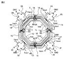
図5は、本発明の1つの実施の形態によるRF電力増幅器の基本的な構成を示す図である。
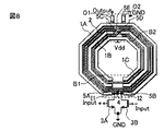
図6は、本発明の実施の形態によるRF電力増幅器の他の構成を示す図である。
図11は、図5で説明したトランスフォーマと1個のプッシュプル型電力増幅回路のNチャンネルMOSトランジスタとをSiチップに集積化した本発明の他の実施の形態によるモノリシックRF電力増幅器の構成を示す図である。
図12は、1個のプッシュプル型電力増幅回路のNチャンネルMOSトランジスタを集積化したSiチップ10と図9で説明した出力インピーダンス整合トランスフォーマ11とを内蔵した本発明の他の実施の形態によるRF電力増幅器モジュールの構成を示す図である。
図15は、図5乃至図13に示した本発明の種々の実施の形態のRF電力増幅器のプッシュプル型電力増幅回路で使用されるLD型MOSトランジスタの構成を示す図である。
図17は、図14に示した本発明の他の実施の形態のRF電力増幅器のプッシュプル型電力増幅回路で使用される高耐圧npn型ヘテロバイポーラトランジスタ(HBT)の構成を示す図である。
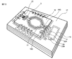
図18は、上記で説明した図5乃至図17に示した本発明の種々の実施の形態を応用した携帯電話端末に使用する具体的なRF電力増幅器モジュールの構成を示す図である。
2 トランスフォーマの二次コイル
3A、3B トランジスタ
Output 出力信号
Vdd 電源電圧
GND 接地電圧
4 容量
5A、5B、5C、5D、5E 下層クロス配線
6A、6B ビア
+Input 非反転入力信号
−Input 反転入力信号
I1、I2 トランスフォーマの入力端子
O1、O2 トランスフォーマの出力端子
C1 中間点
B1 第1部分
B2 第2部分
10 Siチップ
11 トランスフォーマ
12 入力インピーダンス整合トランスフォーマ
13、14、15、16 外部リード
17 プリント基板
18A、18B、18C、18D 容量
19 インダクタ
20、21、22A、22B ビア
40 ヘテロバイポーラトランジスタ
41 GaAsチップ
Claims (34)
- プッシュプル電力増幅回路の能動デバイスとしての第1トランジスタおよび第2トランジスタと、前記プッシュプル電力増幅回路の出力整合回路としてのトランスフォーマとを具備して、
前記第1トランジスタの入力端子と前記第2トランジスタの入力端子とに、非反転入力信号と反転入力信号とがそれぞれ供給可能とされており、
前記トランスフォーマは、磁気的に結合した一次コイルと二次コイルとを有しており、
前記トランスフォーマの前記一次コイルの一端と他端とは、前記第1トランジスタの出力端子と前記第2トランジスタの出力端子にそれぞれ接続され、前記トランスフォーマの前記二次コイルの一端と他端との間から出力信号が生成可能とされており、
前記トランスフォーマの前記一次コイルは、前記第1トランジスタの前記出力端子と前記第2トランジスタの前記出力端子の間に並列に接続されるとともに前記二次コイルと磁気的に結合した第1コイルと第2コイルとを少なくとも含み、
前記二次コイルは、前記一次コイルの前記第1コイルと前記第2コイルとの間に形成されたRF電力増幅器。 - 前記第1コイルと前記第2コイルとの少なくとも一方のコイルは前記第1トランジスタの前記出力端子と前記第2トランジスタの前記出力端子との間で電源電圧が供給可能とされている請求項1に記載のRF電力増幅器。
- 前記トランスフォーマの前記一次コイルと前記二次コイルとは基板の表面に平坦に形成された環状形状の金属薄膜配線によってそれぞれ構成されている請求項2に記載のRF電力増幅器。
- 前記トランスフォーマの前記一次コイルを構成する金属薄膜配線の配線幅は、前記トランスフォーマの前記二次コイルを構成する金属薄膜配線の配線幅よりも大きく形成されている請求項3に記載のRF電力増幅器。
- 前記トランスフォーマの前記一次コイルを構成する前記金属薄膜配線と前記トランスフォーマの前記二次コイルを構成する前記金属薄膜配線とは前記環状形状の周辺にそれぞれ形成されており、
前記一次コイルと前記二次コイルは所定のターン比に設定されることによって、前記トランスフォーマは前記ターン比によって決定されるインピーダンス変換比によって出力整合の動作を実行する請求項4に記載のRF電力増幅器。 - 前記二次コイルのターン数は、前記一次コイルのターン数の略整数倍に設定されている請求項5に記載のRF電力増幅器。
- 前記トランスフォーマの前記一次コイルの前記第1コイルと前記第2コイルとは、前記環状形状の外側金属薄膜配線と内側金属薄膜配線とによってそれぞれ形成されており、
前記二次コイルは、前記外側金属薄膜配線と前記内側金属薄膜配線の間に形成された中央金属薄膜配線によって構成されている請求項5に記載のRF電力増幅器。 - 前記外側金属薄膜配線と前記内側金属薄膜配線との間で前記中央金属薄膜配線によって構成された前記二次コイルは、複数のターン数を形成する請求項7に記載のRF電力増幅器。
- 前記第1コイルと前記二次コイルと前記第2コイルは前記基板の前記表面に形成された多層配線構造によって形成され、前記多層配線構造において前記二次コイルは前記第1コイルと前記第2コイルとにより挟まれている請求項5に記載のRF電力増幅器。
- 前記基板は半導体チップであり、前記第1トランジスタと前記第2トランジスタとは前記半導体チップに形成され、前記トランスフォーマはオンチップトランスフォーマとして前記半導体チップに形成されている請求項5に記載のRF電力増幅器。
- 前記トランスフォーマが形成された前記基板は配線基板であり、前記第1トランジスタと前記第2トランジスタとは半導体チップに形成されており、
前記配線基板に形成された前記トランスフォーマは、前記半導体チップに形成された前記第1トランジスタおよび前記第2トランジスタに接続配線によって電気的に接続されている請求項5に記載のRF電力増幅器。 - 前記トランスフォーマの前記一次コイルは、対称形状で形成されている請求項5に記載のRF電力増幅器。
- 前記第1トランジスタと前記第2トランジスタとはMOSトランジスタである請求項5に記載のRF電力増幅器。
- 前記MOSトランジスタはLD型MOSトランジスタである請求項13に記載のRF電力増幅器。
- 前記第1トランジスタと前記第2トランジスタとはバイポーラトランジスタである請求項5に記載のRF電力増幅器。
- 前記バイポーラトランジスタは化合物半導体へテロバイポーラトランジスタである請求項15に記載のRF電力増幅器。
- 前記第1トランジスタおよび前記第2トランジスタが接続された前記一次コイルの前記一端および前記他端と前記出力信号が生成可能とされた前記二次コイルの前記一端および前記他端は前記環状形状で相互に対向する場所に形成されている請求項1から請求項16までのいずれかに記載のRF電力増幅器。
- プッシュプル電力増幅回路の能動デバイスとしての第1トランジスタおよび第2トランジスタと、前記プッシュプル電力増幅回路の出力整合回路としてのトランスフォーマとを具備して、
前記第1トランジスタの入力端子と前記第2トランジスタの入力端子とに、非反転入力信号と反転入力信号とがそれぞれ供給可能とされており、
前記トランスフォーマは、一次金属薄膜配線と二次金属薄膜配線とを有し、前記一次金属薄膜配線と前記二次金属薄膜配線とは磁気的に結合され、前記一次金属薄膜配線と前記二次金属薄膜配線とは基板の表面に平坦に形成された環状形状をそれぞれ有しており、
前記トランスフォーマの前記一次金属薄膜配線の一端には前記第1トランジスタの出力端子が接続され、前記トランスフォーマの前記一次金属薄膜配線の他端には前記第2トランジスタの出力端子が接続され、
前記トランスフォーマの前記二次金属薄膜配線の一端と他端との間から、出力信号が生成可能とされており、
前記トランスフォーマの前記一次金属薄膜配線の前記一端および前記他端と前記二次金属薄膜配線の前記一端および前記他端とは、前記環状形状で相互に対向する第1部分と第2部分とにそれぞれ形成され、
前記環状形状の前記第1部分において、前記トランスフォーマの前記一次金属薄膜配線の前記一端と前記他端とは互いに近接して配置されており、
前記環状形状の前記第2部分において、前記トランスフォーマの前記二次金属薄膜配線の前記一端と前記他端とは互いに近接して配置されており、
前記トランスフォーマの前記一次金属薄膜配線は前記第1トランジスタの前記出力端子と前記第2トランジスタの前記出力端子の間に並列に接続されるとともに前記二次金属薄膜配線と磁気的に結合した第1配線と第2配線を少なくとも含み、
前記二次金属薄膜配線は、前記一次金属薄膜配線の前記第1配線と前記第2配線との間に形成されたRF電力増幅器。 - 前記第1配線と前記第2配線との少なくとも一方の配線は前記第1トランジスタの前記出力端子と前記第2トランジスタの前記出力端子との間で電源電圧が供給可能とされている請求項18に記載のRF電力増幅器。
- 前記トランスフォーマの前記一次金属薄膜配線の配線幅は、前記トランスフォーマの前記二次金属薄膜配線の配線幅よりも大きく形成されている請求項19に記載のRF電力増幅器。
- 前記トランスフォーマの前記一次金属薄膜配線と前記トランスフォーマの前記二次金属薄膜配線とは前記環状形状の周辺にそれぞれ形成されており、
前記一次金属薄膜配線と前記二次金属薄膜配線は所定のターン比に設定されることによって、前記トランスフォーマは前記ターン比によって決定されるインピーダンス変換比によって出力整合の動作を実行する請求項20に記載のRF電力増幅器。 - 前記二次金属薄膜配線のターン数は前記一次金属薄膜配線のターン数の略整数倍に設定されている請求項21に記載のRF電力増幅器。
- 前記トランスフォーマの前記一次金属薄膜配線の前記第1配線と前記第2配線とは、前記環状形状の外側金属薄膜配線と内側金属薄膜配線とによってそれぞれ形成されており、
前記二次金属薄膜配線は、前記外側金属薄膜配線と前記内側金属薄膜配線の間に形成された中央金属薄膜配線によって構成されている請求項22に記載のRF電力増幅器。 - 前記外側金属薄膜配線と前記内側金属薄膜配線との間で前記中央金属薄膜配線によって構成された前記二次金属薄膜配線は、複数のターン数を形成するものである請求項23に記載のRF電力増幅器。
- 前記第1配線と前記二次金属薄膜配線と前記第2配線は前記基板の前記表面に形成された多層配線構造によって形成され、前記多層配線構造において前記二次金属薄膜配線は前記第1配線と前記第2配線とにより挟まれたものである請求項21に記載のRF電力増幅器。
- 前記基板は半導体チップであり、前記第1トランジスタと前記第2トランジスタとは前記半導体チップに形成され、前記トランスフォーマはオンチップトランスフォーマとして前記半導体チップに形成されている請求項21に記載のRF電力増幅器。
- 前記トランスフォーマが形成された前記基板は配線基板であり、前記第1トランジスタと前記第2トランジスタとは半導体チップに形成されており、
前記配線基板に形成された前記トランスフォーマは、前記半導体チップに形成された前記第1トランジスタおよび前記第2トランジスタに接続配線によって電気的に接続されている請求項21に記載のRF電力増幅器。 - 前記第1トランジスタと前記第2トランジスタとはMOSトランジスタである請求項21に記載のRF電力増幅器。
- 前記MOSトランジスタはLD型MOSトランジスタである請求項28に記載のRF電力増幅器。
- 前記第1トランジスタと前記第2トランジスタとはバイポーラトランジスタである請求項21に記載のRF電力増幅器。
- 前記バイポーラトランジスタは化合物半導体へテロバイポーラトランジスタである請求項30に記載のRF電力増幅器。
- 前記一次金属薄膜配線に接続される前記能動素子として、前記環状形状の前記第1部分において前記トランスフォーマの前記一次金属薄膜配線の前記一端および前記他端に前記第1トランジスタおよび前記第2トランジスタのみが接続されており、
前記第1部分と前記第2部分とを接続する仮想線を中心に前記トランスフォーマの前記一次金属薄膜配線と前記二次金属薄膜配線とは、それぞれ対称形状で形成されている請求項18から請求項31のいずれかに記載のRF電力増幅器。 - 前記電源電圧は、前記一次コイルの対称線上で前記一方のコイルに供給可能とされている請求項12に記載のRF電力増幅器。
- 前記電源電圧は、前記一次コイルの対称線上で前記一方の配線に供給可能とされている請求項19に記載のRF電力増幅器。
Priority Applications (7)
| Application Number | Priority Date | Filing Date | Title |
|---|---|---|---|
| JP2008290911A JP5247367B2 (ja) | 2008-11-13 | 2008-11-13 | Rf電力増幅器 |
| US12/575,494 US7990220B2 (en) | 2008-11-13 | 2009-10-08 | RF power amplifier |
| CN200910222005.8A CN101741326B (zh) | 2008-11-13 | 2009-11-13 | Rf功率放大器 |
| US13/166,312 US8154344B2 (en) | 2008-11-13 | 2011-06-22 | RF power amplifier |
| US13/423,327 US8330545B2 (en) | 2008-11-13 | 2012-03-19 | RF power amplifier |
| US13/677,626 US8514022B2 (en) | 2008-11-13 | 2012-11-15 | RF power amplifier |
| US13/946,219 US8698562B2 (en) | 2008-11-13 | 2013-07-19 | RF power amplifier |
Applications Claiming Priority (1)
| Application Number | Priority Date | Filing Date | Title |
|---|---|---|---|
| JP2008290911A JP5247367B2 (ja) | 2008-11-13 | 2008-11-13 | Rf電力増幅器 |
Publications (2)
| Publication Number | Publication Date |
|---|---|
| JP2010118916A JP2010118916A (ja) | 2010-05-27 |
| JP5247367B2 true JP5247367B2 (ja) | 2013-07-24 |
Family
ID=42164655
Family Applications (1)
| Application Number | Title | Priority Date | Filing Date |
|---|---|---|---|
| JP2008290911A Active JP5247367B2 (ja) | 2008-11-13 | 2008-11-13 | Rf電力増幅器 |
Country Status (3)
| Country | Link |
|---|---|
| US (5) | US7990220B2 (ja) |
| JP (1) | JP5247367B2 (ja) |
| CN (1) | CN101741326B (ja) |
Families Citing this family (74)
| Publication number | Priority date | Publication date | Assignee | Title |
|---|---|---|---|---|
| US8666340B2 (en) * | 2009-03-03 | 2014-03-04 | Broadcom Corporation | Method and system for on-chip impedance control to impedance match a configurable front end |
| WO2010142998A2 (en) * | 2009-06-11 | 2010-12-16 | Imperial Innovations Limited | Radio frequency detector coils |
| US8143952B2 (en) * | 2009-10-08 | 2012-03-27 | Qualcomm Incorporated | Three dimensional inductor and transformer |
| US8264255B2 (en) | 2009-11-03 | 2012-09-11 | Silicon Laboratories Inc. | Radio frequency (RF) power detector suitable for use in automatic gain control (AGC) |
| US8471358B2 (en) * | 2010-06-01 | 2013-06-25 | Taiwan Semiconductor Manufacturing Company, Ltd. | 3D inductor and transformer |
| US9059026B2 (en) | 2010-06-01 | 2015-06-16 | Taiwan Semiconductor Manufacturing Company, Ltd. | 3-D inductor and transformer |
| JP5530265B2 (ja) * | 2010-06-21 | 2014-06-25 | パナソニック株式会社 | 電力増幅器 |
| JP5552691B2 (ja) * | 2010-10-28 | 2014-07-16 | トランスフォーム・ジャパン株式会社 | レギュレータ回路 |
| JP5620804B2 (ja) * | 2010-12-16 | 2014-11-05 | ルネサスエレクトロニクス株式会社 | 高周波電力増幅装置 |
| CN102570994A (zh) * | 2010-12-28 | 2012-07-11 | 沈阳中科微电子有限公司 | 射频功率放大器 |
| US9667206B2 (en) | 2011-02-24 | 2017-05-30 | Dsp Group Ltd. | Linear row array integrated power combiner for RF power amplifiers |
| US8581338B2 (en) | 2011-05-12 | 2013-11-12 | United Microelectronics Corp. | Lateral-diffused metal oxide semiconductor device (LDMOS) and fabrication method thereof |
| EP2745379B1 (en) * | 2011-08-16 | 2019-10-16 | Signify Holding B.V. | A capacitive contactless powering system |
| US8478213B2 (en) | 2011-10-14 | 2013-07-02 | Research In Motion Limited | Methods and apparatus for power control |
| EP2582038B1 (en) * | 2011-10-14 | 2014-12-17 | BlackBerry Limited | Methods and apparatus for power control |
| TWI497907B (zh) * | 2012-02-10 | 2015-08-21 | Univ Nat Taiwan | 變壓式功率放大器 |
| KR101339486B1 (ko) | 2012-03-29 | 2013-12-10 | 삼성전기주식회사 | 박막 코일 및 이를 구비하는 전자 기기 |
| US9172338B2 (en) * | 2012-06-01 | 2015-10-27 | Intel Corporation | Transformer-based RF power amplifier |
| US9124173B2 (en) | 2012-08-20 | 2015-09-01 | International Business Machines Corporation | Slab inductor device providing efficient on-chip supply voltage conversion and regulation |
| CN103679931A (zh) * | 2012-09-07 | 2014-03-26 | 中国移动通信集团贵州有限公司 | 一种射频信号传输电路、非接触式支付终端及支付方法 |
| US9859852B2 (en) | 2012-09-23 | 2018-01-02 | Dsp Group Ltd. | RF power amplifier splitter |
| CN103795352A (zh) * | 2012-10-30 | 2014-05-14 | Dsp集团有限公司 | 包含微调单元的dc-dc转换器 |
| JP5928316B2 (ja) * | 2012-11-26 | 2016-06-01 | 富士通株式会社 | 分配器 |
| DE102013101768A1 (de) | 2013-02-22 | 2014-08-28 | Intel Mobile Communications GmbH | Transformator und elektrische Schaltung |
| US9041152B2 (en) | 2013-03-14 | 2015-05-26 | Taiwan Semiconductor Manufacturing Company, Ltd. | Inductor with magnetic material |
| CN103247426B (zh) * | 2013-06-06 | 2016-09-28 | 电子科技大学 | 一种八路完全对称的分布式片上变压器 |
| EP2838194B1 (en) * | 2013-08-14 | 2017-10-04 | Ampleon Netherlands B.V. | Amplifier circuits |
| JP6291796B2 (ja) * | 2013-11-08 | 2018-03-14 | 株式会社ソシオネクスト | 増幅器 |
| JP6138032B2 (ja) * | 2013-11-21 | 2017-05-31 | 株式会社ThruChip Japan | 集積回路及びそれを備える積層回路 |
| US9553549B2 (en) * | 2014-05-28 | 2017-01-24 | Avago Technologies General Ip (Singapore) Pte. Ltd. | Hybrid power amplifier having electrical and thermal conduction path |
| CN104103636B (zh) * | 2014-07-07 | 2016-08-24 | 武汉芯泰科技有限公司 | 一种片上变压器 |
| US9978732B2 (en) | 2014-09-30 | 2018-05-22 | Skyworks Solutions, Inc. | Network with integrated passive device and conductive trace in packaging substrate and related modules and devices |
| US20160125995A1 (en) * | 2014-10-31 | 2016-05-05 | Qualcomm Incorporated | Array of interleaved 8-shaped transformers with high isolation between adjacent elements |
| US20160233016A1 (en) * | 2015-02-09 | 2016-08-11 | Qualcomm Incorporated | System, apparatus, and method for power amplification transformers |
| CN104767021B (zh) * | 2015-05-04 | 2017-10-03 | 中国电子科技集团公司第五十四研究所 | 一种宽带高平衡度的片上变压器巴伦 |
| CN106304633A (zh) * | 2015-06-10 | 2017-01-04 | 中兴通讯股份有限公司 | 线圈处理方法及终端 |
| TWI541842B (zh) * | 2015-10-23 | 2016-07-11 | 瑞昱半導體股份有限公司 | 螺旋狀堆疊式積體變壓器及電感 |
| KR101719310B1 (ko) * | 2015-10-30 | 2017-03-24 | (주)에프씨아이 | 듀얼 동작 모드 전력 증폭기 |
| JP6418134B2 (ja) * | 2015-11-02 | 2018-11-07 | 株式会社村田製作所 | 電子部品 |
| TWI619128B (zh) | 2015-12-08 | 2018-03-21 | 瑞昱半導體股份有限公司 | 螺旋狀堆疊式積體電感及變壓器 |
| TWI619129B (zh) * | 2015-12-15 | 2018-03-21 | 瑞昱半導體股份有限公司 | 電感結構 |
| KR102484849B1 (ko) * | 2015-12-18 | 2023-01-05 | 주식회사 위츠 | 코일 조립체 |
| JP6621715B2 (ja) | 2016-07-08 | 2019-12-18 | ルネサスエレクトロニクス株式会社 | 無線通信装置及びそれを備えた電力量計測装置 |
| JP6702083B2 (ja) * | 2016-08-23 | 2020-05-27 | 株式会社村田製作所 | 高周波増幅器モジュール |
| JP6710606B2 (ja) * | 2016-08-23 | 2020-06-17 | 株式会社村田製作所 | 高周波増幅器モジュール |
| US10340210B2 (en) * | 2016-09-16 | 2019-07-02 | Texas Instruments Incorporated | System in package device including inductor |
| CN106533374A (zh) * | 2016-09-20 | 2017-03-22 | 锐迪科微电子(上海)有限公司 | 一种多频gsm射频功率放大器 |
| JP2018093339A (ja) * | 2016-12-01 | 2018-06-14 | 住友電気工業株式会社 | 光送信器用駆動回路 |
| TWI634570B (zh) | 2017-06-19 | 2018-09-01 | 瑞昱半導體股份有限公司 | 非對稱式螺旋狀電感 |
| US10110177B1 (en) * | 2017-07-28 | 2018-10-23 | Silicon Laboratories Inc. | Programmable impedance control for a transformer |
| TWI664649B (zh) * | 2017-07-31 | 2019-07-01 | 瑞昱半導體股份有限公司 | 電感裝置 |
| CN108512559B (zh) * | 2018-01-18 | 2024-01-30 | 加特兰微电子科技(上海)有限公司 | 变压器、射频接收装置及其控制方法 |
| US10439575B1 (en) * | 2018-05-24 | 2019-10-08 | Speedlink Technology Inc. | Wideband distributed differential power amplifier utilizing metamaterial transmission line conception with impedance transformation |
| NL2021654B1 (en) * | 2018-09-18 | 2020-05-07 | Prodrive Tech Bv | Balun transformer |
| GB2579215B (en) * | 2018-11-23 | 2023-07-19 | Comet Ag | Broadband power combining arrangement |
| CN111756339A (zh) * | 2018-12-07 | 2020-10-09 | 曹秀妹 | 一种可切换工作功率的双模式功率放大器及模式切换方法 |
| CN109411183A (zh) * | 2018-12-12 | 2019-03-01 | 深圳飞骧科技有限公司 | 双螺旋结构变压器及射频功率放大器 |
| CN109660213A (zh) * | 2018-12-19 | 2019-04-19 | 上海秦芯信息科技有限公司 | 一种应用于5g毫米波基站的功率放大器 |
| US11742130B2 (en) * | 2019-06-24 | 2023-08-29 | Nxp B.V. | High current integrated circuit-based transformer |
| CN110635777B (zh) * | 2019-07-26 | 2023-03-31 | 立安智通(北京)科技有限公司 | 一种宽带天线阻抗变换器设计方法、装置与系统 |
| CN110324015A (zh) * | 2019-07-26 | 2019-10-11 | 成都理工大学 | 一种高功率分布型有源变压合成功率放大器 |
| CN110350877A (zh) * | 2019-07-26 | 2019-10-18 | 成都理工大学 | 一种高增益分布式变压器合成的功率放大器 |
| CN112444767A (zh) * | 2019-08-30 | 2021-03-05 | 通用电气精准医疗有限责任公司 | 用于磁共振成像的射频功率变换器和射频发射系统 |
| JP2021061577A (ja) | 2019-10-09 | 2021-04-15 | 株式会社村田製作所 | 高周波モジュールおよび通信装置 |
| JP2021145283A (ja) | 2020-03-13 | 2021-09-24 | 株式会社村田製作所 | 高周波モジュールおよび通信装置 |
| JP2021145290A (ja) | 2020-03-13 | 2021-09-24 | 株式会社村田製作所 | 高周波モジュールおよび通信装置 |
| JP2021175053A (ja) | 2020-04-22 | 2021-11-01 | 株式会社村田製作所 | 高周波モジュールおよび通信装置 |
| CN111653852B (zh) * | 2020-05-19 | 2021-06-11 | 南京理工大学 | 片上基于变压器的传输零点可调滤波器 |
| US11651887B2 (en) | 2020-05-27 | 2023-05-16 | Infineon Technologies Ag | Stacked and interleaved transformer layout |
| CN111600559B (zh) * | 2020-06-16 | 2021-07-06 | 锐石创芯(深圳)科技有限公司 | 功放输出匹配电路、射频前端模组和无线装置 |
| US20220109405A1 (en) * | 2020-10-02 | 2022-04-07 | Qualcomm Incorporated | Distributed active power combining amplifier |
| CN115549614B (zh) * | 2021-06-30 | 2023-11-24 | 锐石创芯(深圳)科技股份有限公司 | 射频前端模组 |
| CN117375654A (zh) * | 2021-06-30 | 2024-01-09 | 锐石创芯(深圳)科技股份有限公司 | 射频前端模组 |
| CN113593861A (zh) * | 2021-08-09 | 2021-11-02 | 东南大学 | 一种阻抗转换比可调的两路功率合成片上变压器 |
Family Cites Families (9)
| Publication number | Priority date | Publication date | Assignee | Title |
|---|---|---|---|---|
| JPH0377360A (ja) * | 1989-08-18 | 1991-04-02 | Mitsubishi Electric Corp | 半導体装置 |
| JPH0878994A (ja) * | 1994-08-30 | 1996-03-22 | Daihen Corp | インピ−ダンス整合回路 |
| CN1086051C (zh) * | 1995-05-31 | 2002-06-05 | 皇家菲利浦电子有限公司 | 通过变压器的电路偏置 |
| US5781072A (en) * | 1996-09-20 | 1998-07-14 | Motorola, Inc. | Dual push-pull amplifier circuit and method |
| US7245186B2 (en) * | 2004-07-02 | 2007-07-17 | Integrated System Solution Corp. | Bandpass amplifier |
| KR100656335B1 (ko) * | 2005-04-14 | 2006-12-13 | 한국과학기술원 | 전송선 변압기 |
| JP2008278345A (ja) * | 2007-05-02 | 2008-11-13 | Renesas Technology Corp | 半導体装置 |
| US7576607B2 (en) * | 2008-01-03 | 2009-08-18 | Samsung Electro-Mechanics | Multi-segment primary and multi-turn secondary transformer for power amplifier systems |
| US7777570B2 (en) * | 2008-03-12 | 2010-08-17 | Mediatek Inc. | Transformer power combiner having secondary winding conductors magnetically coupled to primary winding conductors and configured in topology including series connection and parallel connection |
-
2008
- 2008-11-13 JP JP2008290911A patent/JP5247367B2/ja active Active
-
2009
- 2009-10-08 US US12/575,494 patent/US7990220B2/en active Active
- 2009-11-13 CN CN200910222005.8A patent/CN101741326B/zh active Active
-
2011
- 2011-06-22 US US13/166,312 patent/US8154344B2/en active Active
-
2012
- 2012-03-19 US US13/423,327 patent/US8330545B2/en active Active
- 2012-11-15 US US13/677,626 patent/US8514022B2/en active Active
-
2013
- 2013-07-19 US US13/946,219 patent/US8698562B2/en active Active
Also Published As
| Publication number | Publication date |
|---|---|
| US20130300505A1 (en) | 2013-11-14 |
| US20100117737A1 (en) | 2010-05-13 |
| US8698562B2 (en) | 2014-04-15 |
| US8154344B2 (en) | 2012-04-10 |
| US20110248782A1 (en) | 2011-10-13 |
| US20120176197A1 (en) | 2012-07-12 |
| US7990220B2 (en) | 2011-08-02 |
| US20130069725A1 (en) | 2013-03-21 |
| US8514022B2 (en) | 2013-08-20 |
| US8330545B2 (en) | 2012-12-11 |
| CN101741326B (zh) | 2014-05-07 |
| JP2010118916A (ja) | 2010-05-27 |
| CN101741326A (zh) | 2010-06-16 |
Similar Documents
| Publication | Publication Date | Title |
|---|---|---|
| JP5247367B2 (ja) | Rf電力増幅器 | |
| US10181834B2 (en) | Baluns for RF signal conversion and impedance matching | |
| US7675365B2 (en) | Systems and methods for power amplifiers with voltage boosting multi-primary transformers | |
| US7936215B2 (en) | Multi-segment primary and multi-turn secondary transformer for power amplifier systems | |
| Zhao et al. | A 40-nm CMOS E-band 4-way power amplifier with neutralized bootstrapped cascode amplifier and optimum passive circuits | |
| US9082543B2 (en) | Inductor | |
| Thian et al. | A 76–84 GHz SiGe power amplifier array employing low-loss four-way differential combining transformer | |
| JP2008278345A (ja) | 半導体装置 | |
| TWI404085B (zh) | 變壓器及其結構與功率放大裝置 | |
| US10236841B2 (en) | Differential amplifier | |
| US20220321067A1 (en) | Low noise amplifier incorporating sutardja transformer | |
| US10243522B2 (en) | Fully integrated low-noise amplifier | |
| US11888459B2 (en) | Balun with improved common mode rejection ratio | |
| CN116232235A (zh) | 集成射频功率放大器和射频设备 | |
| Arrawatia et al. | A CMOS power amplifier with 180° hybrid on-chip coupler for 4G applications | |
| EP4200980A1 (en) | Power combiner for amplifier arrangement | |
| Bakalski et al. | A monolithic 2.45 GHz, 0.56 W power amplifier with 45% PAE at 2.4 V in standard 25 GHz f/sub T/Si-bipolar |
Legal Events
| Date | Code | Title | Description |
|---|---|---|---|
| A711 | Notification of change in applicant |
Free format text: JAPANESE INTERMEDIATE CODE: A712 Effective date: 20100527 |
|
| A621 | Written request for application examination |
Free format text: JAPANESE INTERMEDIATE CODE: A621 Effective date: 20111101 |
|
| A977 | Report on retrieval |
Free format text: JAPANESE INTERMEDIATE CODE: A971007 Effective date: 20120820 |
|
| A131 | Notification of reasons for refusal |
Free format text: JAPANESE INTERMEDIATE CODE: A131 Effective date: 20120830 |
|
| A521 | Request for written amendment filed |
Free format text: JAPANESE INTERMEDIATE CODE: A523 Effective date: 20121015 |
|
| TRDD | Decision of grant or rejection written | ||
| A01 | Written decision to grant a patent or to grant a registration (utility model) |
Free format text: JAPANESE INTERMEDIATE CODE: A01 Effective date: 20130314 |
|
| A61 | First payment of annual fees (during grant procedure) |
Free format text: JAPANESE INTERMEDIATE CODE: A61 Effective date: 20130409 |
|
| R150 | Certificate of patent or registration of utility model |
Ref document number: 5247367 Country of ref document: JP Free format text: JAPANESE INTERMEDIATE CODE: R150 Free format text: JAPANESE INTERMEDIATE CODE: R150 |
|
| FPAY | Renewal fee payment (event date is renewal date of database) |
Free format text: PAYMENT UNTIL: 20160419 Year of fee payment: 3 |
|
| S531 | Written request for registration of change of domicile |
Free format text: JAPANESE INTERMEDIATE CODE: R313531 |
|
| R350 | Written notification of registration of transfer |
Free format text: JAPANESE INTERMEDIATE CODE: R350 |