JP4906030B2 - テスト回路およびテスト方法 - Google Patents
テスト回路およびテスト方法 Download PDFInfo
- Publication number
- JP4906030B2 JP4906030B2 JP2004300959A JP2004300959A JP4906030B2 JP 4906030 B2 JP4906030 B2 JP 4906030B2 JP 2004300959 A JP2004300959 A JP 2004300959A JP 2004300959 A JP2004300959 A JP 2004300959A JP 4906030 B2 JP4906030 B2 JP 4906030B2
- Authority
- JP
- Japan
- Prior art keywords
- output
- circuit
- clock
- serial data
- test
- Prior art date
- Legal status (The legal status is an assumption and is not a legal conclusion. Google has not performed a legal analysis and makes no representation as to the accuracy of the status listed.)
- Expired - Fee Related
Links
Images


Landscapes
- Tests Of Electronic Circuits (AREA)
- Semiconductor Integrated Circuits (AREA)
Description
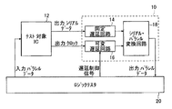
遅延制御信号に応じて、前記集積回路から出力されるシリアルデータとクロックとを相対的かつ可変的に遅延して出力する遅延可変回路と、
前記遅延可変回路から出力されるクロックを用いて、前記遅延可変回路から出力されるシリアルデータをパラレルデータに変換するシリアル・パラレル変換回路とを備え、当該変換されたパラレルデータを判定することにより前記シリアルデータとクロックとの間のセットアップタイムおよびホールドタイムのテストを行うことを特徴とするテスト回路を提供する。
前記出力されるシリアルデータとクロックとを相対的かつ可変的に遅延し、該遅延されたクロックを用いて該遅延されたシリアルデータをパラレルデータに変換し、当該変換されたパラレルデータを判定することにより前記シリアルデータとクロックとの間のセットアップタイムおよびホールドタイムのテストを行うことを特徴とする集積回路のテスト方法を提供する。
ここで、前記出力されるシリアルデータとクロックとを相対的かつ可変的に遅延する機能と、遅延されたシリアルデータをパラレルデータに変換する機能とを、前記半導体集積回路とは別のテスト回路として構成したことが好ましい。
以上、本発明の集積回路のテスト回路およびテスト方法について詳細に説明したが、本発明は上記実施形態に限定されず、本発明の主旨を逸脱しない範囲において、種々の改良や変更をしてもよいのはもちろんである。
12 テスト対象IC
14、34 固定遅延回路
16、36 可変遅延回路
18、38 シリアル・パラレル変換回路
20 ロジックテスタ
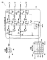
40、42a、42b、42c、42d、54a、54b、54c、54d、56a、56b、56c、56d バッファ回路
44 マルチプレクサ
46、48a、48b、50a、50b、50c、50d、52a、52b、52c、52d フリップフロップ
Claims (3)
- パラレルデータをクロックに同期してシリアルデータに変換し、該シリアルデータおよび該シリアルデータに同期したクロックを出力する機能を有する集積回路のテスト回路であって、
遅延制御信号に応じて、前記集積回路から出力されるシリアルデータとクロックとを相対的かつ可変的に遅延して出力する遅延可変回路と、
前記遅延可変回路から出力されるクロックを用いて、前記遅延可変回路から出力されるシリアルデータをパラレルデータに変換するシリアル・パラレル変換回路とを備え、当該変換されたパラレルデータを判定することにより前記シリアルデータとクロックとの間のセットアップタイムおよびホールドタイムのテストを行うことを特徴とするテスト回路。 - パラレルデータをクロックに同期してシリアルデータに変換し、該シリアルデータおよび該シリアルデータに同期したクロックを出力する機能を有する集積回路のテスト方法であって、
前記出力されるシリアルデータとクロックとを相対的かつ可変的に遅延し、該遅延されたクロックを用いて該遅延されたシリアルデータをパラレルデータに変換し、当該変換されたパラレルデータを判定することにより前記シリアルデータとクロックとの間のセットアップタイムおよびホールドタイムのテストを行うことを特徴とする集積回路のテスト方法。 - 前記出力されるシリアルデータとクロックとを相対的かつ可変的に遅延する機能と、遅延されたシリアルデータをパラレルデータに変換する機能とを、前記半導体集積回路とは別のテスト回路として構成したことを特徴とする請求項2記載の集積回路のテスト方法。
Priority Applications (1)
| Application Number | Priority Date | Filing Date | Title |
|---|---|---|---|
| JP2004300959A JP4906030B2 (ja) | 2004-10-15 | 2004-10-15 | テスト回路およびテスト方法 |
Applications Claiming Priority (1)
| Application Number | Priority Date | Filing Date | Title |
|---|---|---|---|
| JP2004300959A JP4906030B2 (ja) | 2004-10-15 | 2004-10-15 | テスト回路およびテスト方法 |
Publications (3)
| Publication Number | Publication Date |
|---|---|
| JP2006112931A JP2006112931A (ja) | 2006-04-27 |
| JP2006112931A5 JP2006112931A5 (ja) | 2007-10-04 |
| JP4906030B2 true JP4906030B2 (ja) | 2012-03-28 |
Family
ID=36381554
Family Applications (1)
| Application Number | Title | Priority Date | Filing Date |
|---|---|---|---|
| JP2004300959A Expired - Fee Related JP4906030B2 (ja) | 2004-10-15 | 2004-10-15 | テスト回路およびテスト方法 |
Country Status (1)
| Country | Link |
|---|---|
| JP (1) | JP4906030B2 (ja) |
Families Citing this family (4)
| Publication number | Priority date | Publication date | Assignee | Title |
|---|---|---|---|---|
| KR100728654B1 (ko) | 2005-12-02 | 2007-06-14 | 주식회사 애트랩 | 시간-디지털 변환 회로 |
| US8261619B2 (en) | 2005-11-28 | 2012-09-11 | Atlab Inc. | Time to digital converting circuit and pressure sensing device using the same |
| KR100845323B1 (ko) | 2007-04-27 | 2008-07-10 | 주식회사 애트랩 | 아날로그-디지털 변환기 |
| JP5113624B2 (ja) * | 2007-05-24 | 2013-01-09 | 株式会社アドバンテスト | 試験装置 |
Family Cites Families (6)
| Publication number | Priority date | Publication date | Assignee | Title |
|---|---|---|---|---|
| JP2614345B2 (ja) * | 1990-04-20 | 1997-05-28 | 株式会社東芝 | スキャンフリップフロップ |
| JP2962213B2 (ja) * | 1996-01-17 | 1999-10-12 | 日本電気株式会社 | 半導体集積回路のテスト回路およびテスト方法 |
| JP3733389B2 (ja) * | 1999-02-08 | 2006-01-11 | 富士通株式会社 | 半導体集積回路装置及びそのテスト方法 |
| KR20010050814A (ko) * | 1999-10-01 | 2001-06-25 | 하이든 마틴 | 소스 동기 신호의 검사 방법 및 장치 |
| JP2003004821A (ja) * | 2001-06-25 | 2003-01-08 | Hitachi Electronics Eng Co Ltd | 半導体試験方法及び半導体試験装置 |
| JP4208127B2 (ja) * | 2003-06-02 | 2009-01-14 | パナソニック株式会社 | 半導体集積回路装置 |
-
2004
- 2004-10-15 JP JP2004300959A patent/JP4906030B2/ja not_active Expired - Fee Related
Also Published As
| Publication number | Publication date |
|---|---|
| JP2006112931A (ja) | 2006-04-27 |
Similar Documents
| Publication | Publication Date | Title |
|---|---|---|
| US7509517B2 (en) | Clock transferring apparatus for synchronizing input data with internal clock and test apparatus having the same | |
| US6421801B1 (en) | Testing IO timing in a delay locked system using separate transmit and receive loops | |
| KR100870037B1 (ko) | 테스트가 용이한 반도체 장치, 반도체 장치 테스트 방법,반도체 장치 테스트를 위한 테스트 클럭 생성 방법 및 장치 | |
| US8065549B2 (en) | Scan-based integrated circuit having clock frequency divider | |
| US20100039157A1 (en) | Clock adjusting circuit and semiconductor integrated circuit device | |
| US7941720B2 (en) | Scan test circuit and scan test control method | |
| US20070047337A1 (en) | Interface circuit and semiconductor device | |
| JP5181499B2 (ja) | Scanテスト回路及び半導体集積回路 | |
| US20080205170A1 (en) | Ddr-sdram interface circuitry, and method and system for testing the interface circuitry | |
| JP2007108172A (ja) | 半導体回路のオンチップ特性を測定するための装置及びそれに関する方法 | |
| US20160349318A1 (en) | Dynamic Clock Chain Bypass | |
| JP5186485B2 (ja) | 試験装置 | |
| JP4906030B2 (ja) | テスト回路およびテスト方法 | |
| JP5274660B2 (ja) | タイミング発生器および試験装置 | |
| JP4191185B2 (ja) | 半導体集積回路 | |
| US6898741B2 (en) | Arrangements for self-measurement of I/O timing | |
| US20100033189A1 (en) | Semiconductor integrated circuit and test method using the same | |
| KR100714482B1 (ko) | 반도체 장치, 테스트 기판, 반도체 장치의 테스트 시스템및 반도체 장치의 테스트 방법 | |
| US20180156870A1 (en) | Test apparatus | |
| WO2004031788A1 (ja) | マルチストローブ装置、試験装置、及び調整方法 | |
| US20100060323A1 (en) | Test circuit and test method | |
| JP3891913B2 (ja) | 半導体集積回路およびそのテスト方法 | |
| JP2004053412A (ja) | 半導体集積回路試験装置 | |
| JP6530288B2 (ja) | 半導体装置および半導体装置のテスト方法 | |
| JP4820808B2 (ja) | データ出力回路 |
Legal Events
| Date | Code | Title | Description |
|---|---|---|---|
| A521 | Request for written amendment filed |
Free format text: JAPANESE INTERMEDIATE CODE: A523 Effective date: 20070820 |
|
| A621 | Written request for application examination |
Free format text: JAPANESE INTERMEDIATE CODE: A621 Effective date: 20070820 |
|
| A131 | Notification of reasons for refusal |
Free format text: JAPANESE INTERMEDIATE CODE: A131 Effective date: 20110125 |
|
| TRDD | Decision of grant or rejection written | ||
| A01 | Written decision to grant a patent or to grant a registration (utility model) |
Free format text: JAPANESE INTERMEDIATE CODE: A01 Effective date: 20120104 |
|
| A01 | Written decision to grant a patent or to grant a registration (utility model) |
Free format text: JAPANESE INTERMEDIATE CODE: A01 |
|
| A61 | First payment of annual fees (during grant procedure) |
Free format text: JAPANESE INTERMEDIATE CODE: A61 Effective date: 20120106 |
|
| FPAY | Renewal fee payment (event date is renewal date of database) |
Free format text: PAYMENT UNTIL: 20150120 Year of fee payment: 3 |
|
| R150 | Certificate of patent or registration of utility model |
Ref document number: 4906030 Country of ref document: JP Free format text: JAPANESE INTERMEDIATE CODE: R150 Free format text: JAPANESE INTERMEDIATE CODE: R150 |
|
| S111 | Request for change of ownership or part of ownership |
Free format text: JAPANESE INTERMEDIATE CODE: R313111 |
|
| R350 | Written notification of registration of transfer |
Free format text: JAPANESE INTERMEDIATE CODE: R350 |
|
| R250 | Receipt of annual fees |
Free format text: JAPANESE INTERMEDIATE CODE: R250 |
|
| R250 | Receipt of annual fees |
Free format text: JAPANESE INTERMEDIATE CODE: R250 |
|
| R250 | Receipt of annual fees |
Free format text: JAPANESE INTERMEDIATE CODE: R250 |
|
| R250 | Receipt of annual fees |
Free format text: JAPANESE INTERMEDIATE CODE: R250 |
|
| R250 | Receipt of annual fees |
Free format text: JAPANESE INTERMEDIATE CODE: R250 |
|
| LAPS | Cancellation because of no payment of annual fees |