JP4776767B2 - Method for manufacturing semiconductor device - Google Patents
Method for manufacturing semiconductor device Download PDFInfo
- Publication number
- JP4776767B2 JP4776767B2 JP2000327179A JP2000327179A JP4776767B2 JP 4776767 B2 JP4776767 B2 JP 4776767B2 JP 2000327179 A JP2000327179 A JP 2000327179A JP 2000327179 A JP2000327179 A JP 2000327179A JP 4776767 B2 JP4776767 B2 JP 4776767B2
- Authority
- JP
- Japan
- Prior art keywords
- island
- layer
- film
- semiconductor layer
- shaped
- Prior art date
- Legal status (The legal status is an assumption and is not a legal conclusion. Google has not performed a legal analysis and makes no representation as to the accuracy of the status listed.)
- Expired - Fee Related
Links
Images


Description
【0001】
【発明の属する技術分野】
本発明は、絶縁表面を有する基板上に形成する結晶構造を有する半導体膜の作製方法、並びに該半導体膜を活性層に用いた半導体装置の作製方法に関する。特に、結晶質半導体で活性層を形成した薄膜トランジスタの作製方法に関する。尚、本明細書中において半導体装置とは、半導体特性を利用することで機能しうる装置全般を指し、薄膜トランジスタを用いて形成されるアクティブマトリクス駆動方式の液晶表示装置に代表される電気光学装置、およびそのような電気光学装置を部品として搭載した電子機器を範疇とする。
【0002】
【従来の技術】
絶縁表面を有する透光性基板上に非晶質半導体膜を形成し、レーザーアニール法やファーネスアニール炉を用いた熱処理(以下、熱アニール法と呼ぶ)で結晶化させた結晶質半導体膜を薄膜トランジスタ(Thin Film Transistor:以下、TFTと記す)の活性層に用いる技術が開発されている。絶縁表面を有する透光性基板には、バリウムホウケイ酸ガラスやアルミノホウケイ酸ガラスなどのガラス基板が多くの場合用いられている。このようなガラス基板は石英基板と比べ耐熱性は劣るものの市販価格は安価であり、また大面積基板を容易に製造できる利点を有している。
【0003】
レーザーアニール法はガラス基板の温度をあまり上昇させず、非晶質半導体膜にのみ高いエネルギーを与えて結晶化させることができる結晶化技術として知られている。特に、波長400nm以下の短波長光を発振するエキシマレーザーは、このレーザーアニール法の開発当初から用いられてきた代表的なレーザーである。近年ではその他に固体レーザーのYAGレーザーを用いる技術も開発されている。これらのレーザーアニール法は、レーザービームを被照射面においてスポット状や線状となるように光学系で加工し、その加工されたレーザー光で基板上の被照射面を走査すること(レーザー光の照射位置を被照射面に対して相対的に移動させる)により行う。例えば、線状レーザー光を用いたエキシマレーザーアニール法は、その長手方向と直角な方向だけの走査で被照射面全体をレーザーアニールすることも可能であり、生産性に優れることからTFTを用いる液晶表示装置の製造技術として主流となりつつある。その技術は一枚のガラス基板上に画素部を形成するTFT(画素TFT)と、画素部の周辺に設けられる駆動回路のTFTを形成したモノシリック型の液晶表示装置を可能とした。
【0004】
しかし、非晶質半導体膜をレーザーアニールして作製される結晶質半導体膜は複数の結晶粒が集合したものであり、その結晶粒の位置と大きさはランダムなものであった。ガラス基板上に作製されるTFTは、素子分離のために結晶質半導体層を島状のパターンに分離して形成している。その場合、結晶粒の位置や大きさを指定して形成することはできなかった。結晶粒の界面(結晶粒界)には、非晶質構造や結晶欠陥などに起因する再結合中心や捕獲中心や結晶粒界におけるポテンシャル準位の影響により、キャリアの電流輸送特性が低下させる原因があることが知られている。しかし、結晶の性質がTFTの特性に重大な影響を及ぼすチャネル形成領域を、結晶粒界の影響を排除して単一の結晶粒で形成することは殆ど不可能であった。そのため結晶質シリコン膜を活性層とするTFTは、単結晶シリコン基板に作製されるMOSトランジスタの特性と同等なものは今日まで得られていない。
【0005】
このような問題点を解決するために、結晶粒を大きく成長させる試みがなされている。例えば、「"High-Mobility Poly-Si Thin-Film Transistors Fabricated by a Novel Excimer Laser Crystallization Method", K.Shimizu, O.Sugiura and M.Matumura, IEEE Transactions on Electron Devices vol.40, No.1, pp112-117,1993」には、基板上にSi/SiO2/Siの3層構造の膜を形成し、エキシマレーザー光をその膜側と基板側の両側から照射するレーザーアニール法についての報告がある。その方法によれば、ある所定のエネルギー強度でレーザー光を照射することにより結晶粒の大粒形化を図ることができることが示されている。
【0006】
【発明が解決しようとする課題】
上記Ishiharaらの方法は、非晶質シリコン膜の下地材料の熱特性を局所的に変化させて、基板への熱の流れを制御して温度勾配を持たせることを特徴としている。しかしながら、そのためにガラス基板上に高融点金属層/酸化シリコン層/半導体膜の3層構造を形成している。この半導体膜を活性層としてトップゲート型のTFTを形成することは構造的には可能であるが、半導体膜と高融点金属層との間に設けられた酸化シリコン膜により寄生容量が発生するので、消費電力が増加し、TFTの高速動作を実現することは困難となる。
【0007】
一方、高融点金属層をゲート電極とすることにより、ボトムゲート型または逆スタガ型のTFTに対しては有効に適用できうると考えられる。しかし、前記3層構造において、半導体膜の厚さを除いたとしても、高融点金属層と酸化シリコン層の膜厚は、結晶化工程において適した膜厚と、TFT素子としての特性において適した膜厚とは必ずしも一致しないので、結晶化工程における最適設計と素子構造の最適設計とを両方同時に満足することはできない。
【0008】
また、透光性のない高融点金属層をガラス基板の全面に形成すると、透過型の液晶表示装置を製作することは不可能である。高融点金属層は熱伝導率が高いという点では有用であるが、高融点金属材料として使用されるクロム(Cr)膜やチタン(Ti)膜は内部応力が高いので、ガラス基板との密着性に問題が生じる可能性が高い。さらに、内部応力の影響はこの上層に形成する半導体膜へも及び、形成された結晶性半導体膜に歪みを与える力として作用する可能性が大きい。
【0009】
一方、TFTにおいて重要な特性パラメータであるしきい値電圧(以下、Vthと記す)を所定の範囲内に制御するためには、チャネル形成領域の価電子制御の他に、活性層に密接して絶縁膜で形成する下地膜やゲート絶縁膜の荷電欠陥密度を低減さることや、その内部応力のバランスを考慮する必要があつた。このような要求に対して、酸化シリコン膜や酸化窒化シリコン膜などのシリコンを構成元素として含む材料が適していた。従って、温度勾配を持たせるために高融点金属層を設けることは、そのバランスを崩してしまうことが懸念される。
【0010】
本発明はこのような問題点を解決するための技術であり、結晶粒の位置とその大きさを制御した結晶質半導体膜を作製し、さらにその結晶質半導体膜をTFTのチャネル形成領域に用いることにより高速動作が可能なTFTを実現する。さらに、そのようなTFTを透過型の液晶表示装置やエレクトロルミネッセンス材料を持った表示装置などのさまざまな半導体装置に適用できる技術を提供することを目的とする。
【0011】
【課題を解決するための手段】
ガラスなどの基板上に形成した非晶質半導体層から結晶質半導体層を形成する方法にレーザーアニール法を用いる。本発明のレーザーアニール法は、パルス発振型または連続発光型のエキシマレーザー、YAGレーザー、またはアルゴンレーザーをその光源とし、光学系にて線状または矩形状に形成されたレーザー光を島状半導体層に対して、島状半導体層が形成された基板の表側(本明細書中では島状半導体層が形成されている面と定義する)と裏側(本明細書中では島状半導体層が形成された面と反対側の面と定義する)との両方から照射する。
【0012】
図2(A)は本発明のレーザーアニール装置の構成を示す図である。レーザーアニール装置は、レーザー発振器1201、光学系1100、基板を固定するステージ1202を有し、ステージ1202にはヒータ1203とヒータコントローラー1204が付加されて、基板を100〜450℃まで加熱することができる。ステージ1202上には反射板1205が設けられ、その上に基板1206を設置する。図2(A)における構成のレーザーアニール装置の構成において、基板1206の保持方法を図2(B)を用いて説明する。ステージ1202に保持された基板1206は、反応室1213に設置されレーザー光が照射される。反応室内は図示されていない排気系またはガス系により減圧状態または不活性ガス雰囲気とすることが可能な構成とし、半導体膜を汚染させることなく100〜450℃まで加熱することができる。ステージ1202はガイドレール1216に沿って反応室内を移動することができ、基板の全面に線状レーサー光を照射させることができる。レーザー光は基板1206の上面に設けられた図示されていない石英製の窓から入射する。また、図2(B)ではこの反応室1213にトランスファー室1210、中間室1211、ロード・アンロード室1212が接続し、仕切弁1217、1218で分離されている。ロード・アンロード室1212には複数の基板を保持することが可能なカセット1214が設置され、トランスファー室1210に設けられた搬送機構1215により基板が搬送される。基板1206'は搬送中の基板を表す。こうのうような構成とすることによりレーザーアニールを減圧下または不活性ガス雰囲気中で連続して処理することができる。
【0013】
図3は図2(A)で示したレーザーアニール装置の光学系1100の基本的な構成を説明する図である。レーザー発振器1101にはエキシマレーザーやYAGレーザー、またはアルゴンレーザーなどを適用する。図3(A)は光学系1100を側面から見た図であり、レーザー発振器1101から出たレーザー光はシリンドリカルレンズアレイ1102により縦方向に分割される。この分割されたレーザー光はシリンドリカルレンズ1104により、一旦集光された後広がって、ミラー1107で反射され、その後、シリンドリカルレンズ1108により照射面1109で線状レーザー光となるようにする。これにより、線状レーザー光の幅方向のエネルギー分布の均一化を図ることができる。また、図3(B)は光学系1100を上面から見た図であり、レーザー発振器1101から出たレーザー光はシリンドリカルレンズアレイ1103により横方向に分割される。その後、シリンドリカルレンズ1105により、レーザー光は照射面1109で一つに合成される。これにより、線状レーザー光の長手方向のエネルギー分布の均一化を図ることができる。
【0014】
図1は本発明のレーザーアニール法の概念を説明する図である。ガラスなどの基板1001上にストライプ状または短冊状の第1の絶縁層1002が形成され、その上に第2の絶縁層1003が形成されている。さらにその上に島状半導体層1004が形成されている。第1の絶縁層1002及び第2の絶縁層1003は酸化シリコン膜や窒化シリコン膜、酸化窒化シリコン膜、およびアルミニウムを成分とする絶縁膜などを適用し、これらの膜単体か若しくは適宣組み合わせて用いる。
【0015】
そして、図3(A)、(B)で説明した光学系1100により、シリンドリカルレンズ1108と同等の機能を有するシリンドリカルレンズ1006を通過したレーザー光は線状レーザー光として島状半導体層1004に照射される。島状半導体層1004には、シリンドリカルレンズ1006を通過して直接島状半導体層1004に照射する第1のレーザー光成分1007と、第1の絶縁層1002と第2の絶縁層1003と基板1001を透過して、反射板1005で反射して、再度基板1001と第1の絶縁層1002と第2の絶縁層1003を透過して島状半導体層1004へ照射される第2のレーザー光成分1008がある。いずれにしても、シリンドリカルレンズ1006を通過したレーザー光は、集光される過程で基板表面に対し、45〜90°の入射角を持つので、反射板1005で反射するレーザー光は、島状半導体層1004の内側の方向にも反射する。反射板1005はアルミニウム(Al)、チタン(Ti)、窒化チタン(TiN)、クロム(Cr)、タングステン(W)、窒化タングステン(WN)などで反射表面を形成する。このように、反射表面を形成する材料を適宣選択することにより、その反射率を20〜90%の範囲で変化させることができ、基板1001の裏側から入射するレーザー光の強度を変化させることができる。また、この反射表面を鏡面にしておくと、240〜320nmの波長範囲で約90%の正反射率が得られる。また、材質をアルミニウムとして、その表面に数100nmの微細な凹凸形状を形成しておくと、拡散反射率(積分反射率―正反射率)は50〜70%が得られる。
【0016】
このようにして、レーザー光は基板1001の表面と裏面から照射され、この基板1001上に形成された島状半導体層1004は両面からレーザーアニールされることになる。レーザーアニール法では、照射するレーザー光の条件を最適なものとすることにより半導体膜を瞬時に加熱して溶融させ、結晶核の発生密度とその結晶核からの結晶成長を制御しようとしている。パルス発振するエキシマレーザーやYAGレーザーの発振パルス幅は数nsec〜数十nsec、例えば30nsecであるので、パルス発振周波数を30Hzとして照射すると、そのレーザー光が照射された領域の半導体層はパルスレーザー光により瞬時に加熱され、その加熱時間よりも遥かに長い時間冷却されることになる。
【0017】
基板上に形成された島状半導体層に対して、一方の面のみからのレーザー光の照射では、片側しか加熱されないので、加熱溶融と冷却固化のサイクルは急峻なものとなり、結晶核の発生密度を制御できたとしても十分な結晶成長は期待できない。しかし、半導体層の両方の面からレーザー光を照射するとこの加熱溶融と冷却固化のサイクルが緩やかなものとなり、冷却固化の過程で結晶成長に許容される時間が相対的に長くなることにより、充分な結晶成長を得ることができる。
【0018】
その過渡的な現象において、島状半導体層に温度分布をもたせ、温度変化の緩やかな領域を設け核生成速度と核生成密度を制御することにより、結晶粒の大粒形化を図る。具体的には、図1で示すように、基板1001上にストライプ状の第1の絶縁層1002を設け、その上に第2の絶縁層1003を形成する。島状半導体層1004は第2の絶縁層1003上に形成されるが、第1の絶縁層1002と交差するようにを設ける。即ち、島状半導体層1004の下側に第2の絶縁層1003が形成されている領域と、第1の絶縁層1002と第2の絶縁層1003の絶縁膜が形成されている領域とを設ける。後者の領域は体積が増え熱容量が大きくなるので、レーザー光の照射による到達最高温度は前者の領域に比べ低くなる。その結果、後者の領域で結晶核の生成が優先的に発生し、この部分より結晶成長が始まる。この時、半導体層の両方の面からレーザー光を照射して、半導体層が十分加熱されていることも重要なファクターとなる。島状半導体層のパルスレーザー光の照射による温度変化のサイクルを緩やかなものとすることにより結晶粒の大粒形化を実現している。
【0019】
島状半導体層を一方の側の面に形成した基板の表面側と裏面側からレーザー光を照射する方法は、図4に示す構成を用いても良い。エキシマレーザーやYAGレーザーなどのレーザー発振器401から出た光はシリンドリカルレンズアレイ402(または403)により分割される。この分割されたレーザー光はシリンドリカルレンズ404(または405)により一旦集光された後広がってミラー408で反射される。この光路の途中にビームスプリッタ406を置き、光路を2分割する。一方のレーザー光はミラー407、413で反射され、シリンドリカルレンズ414により線状レーザー光とされ、基板418の表側に照射する。このレーザー光を第1のレーザー光とする。基板418の表側には下地膜419、島状半導体層420が形成されている。他方のレーザー光はミラー408、409、411で反射され、シリンドリカルレンズ412により線状レーザー光とされ、基板418の裏側に照射する。このレーザー光を第2のレーザー光とする。この光路の途中にはレーザー光の強度を調節するためにアッテネータ410が設けられている。このような構成として、基板の表側と裏側からレーザー光を照射しても、前述と同様に半導体層の結晶粒の大粒形化をすることができる。
【0020】
本明細書では、図1や図4に示す構成のレーザーアニール法をデュアルビームレーザーアニール法と呼び、この方法を適用して島状半導体層の結晶粒の大粒形化を行う。その島状半導体層をTFTの活性層に用いて、さらに各回路の機能に応じた構造を有するTFTを有する半導体装置を作製することにより半導体装置の高性能化を図る。
【0021】
そして、デュアルビームレーザーアニール法を用いる本発明の構成は、透光性基板の一方の面にストライプ状の第1の絶縁層と、該ストライプ状の第1の絶縁層上に第2の絶縁層が設けられる。これらの絶縁層上に設けられる島状半導体層は、ストライプ状の第1の絶縁層と交差して形成される。本発明の好ましい実施形態として、複数本のストライプ状の第1の絶縁層を形成し、島状半導体層を該複数本のストライプ状の第1の絶縁層と交差するように形成し、選択された一本のストライプ状の第1の絶縁層とそれに隣接するストライプ状の第1の絶縁層との間でTFTのチャネル形成領域を形成する。
【0022】
以上のように、本発明の構成は、透光性基板の一方の表面に、島状半導体層と、該島状半導体層の下方に設けられた短冊状の第1の絶縁層とを有し、短冊状の第1の絶縁層は島状半導体層と交差するように設けられていることを特徴としている。第1の絶縁層は一対を成して形成しても良く、一対の短冊状の第1の絶縁層は該島状半導体層と交差するように設けられる。
【0023】
上記構成はTFTに好適に適用することができ、前記島状半導体層に形成される前記薄膜トランジスタのチャネル形成領域は、前記短冊状の第1の絶縁層に隣接して形成し、または、TFTのチャネル形成領域を、一対の短冊状の第1の絶縁層の間に形成することを特徴としている。
【0024】
また、本発明の半導体装置の作製方法は、透光性基板の一方の表面に短冊状の第1の絶縁層を形成する工程と、前記短冊状の第1の絶縁層上に、該短冊状の第1の絶縁層と交差するように島状半導体層を形成する工程と、前記透光性基板の一方の表面側と、他方の表面側とから、前記島状半導体層にレーザー光を照射して、該島状半導体層を結晶化させる工程とを有することを特徴とする。
【0025】
また、他の発明の構成は、透光性基板の一方の表面に一対の短冊状の第1の絶縁層を形成する工程と、前記一対の短冊状の第1の絶縁層上に、該一対の短冊状の第1の絶縁層と交差するように島状半導体層を形成する工程と、前記透光性基板の一方の表面側と、他方の表面側とから、前記島状半導体層にレーザー光を照射して、該島状半導体層を結晶化させる工程とを有することを特徴としている。
【0026】
【発明の実施の形態】
[実施形態1]
本発明の実施形態を図5と図6を用いて説明する。図5(A)において、基板501にはバリウムホウケイ酸ガラスやアルミノホウケイ酸ガラスなどの無アルカリガラス基板を用いる。例えば、コーニング社の#7059ガラスや#1737ガラス基などを好適に用いることができる。
【0027】
この基板501のTFTを形成する表面に、透光性でかつ絶縁性を有する第1の絶縁層502、503を形成する。この第1の絶縁層は熱伝導性の優れる材料で形成しても良い。その場合、熱伝導率は10Wm-1K-1以上であること望ましい。そのような材料として、アルミニウムの酸化物(酸化アルミニウム(Al2O3)は可視光において透光性を有し、熱伝導率が20Wm-1K-1であり適している。また、酸化アルミニウムは化学量論比に限定されるものでなく、熱伝導率特性と内部応力などの特性を制御するために、他の元素を添加しても良い。例えば、酸化アルミニウムに窒素を含ませて、酸化窒化アルミニウム(AlNxO1-x:0.02≦x≦0.5)を用いても良いし、アルミニウムの窒化物(AlNx)を用いることも可能である。また、シリコン(Si)、酸素(O)、窒素(N)とM(Mはアルミニウム(Al)または希土類元素から選ばれた少なくとも一種)を含む化合物を用いることができる。例えば、AlSiONやLaSiONなどを好適に用いることができる。その他に、窒化ホウ素なども適用することができる。
【0028】
上記の酸化物、窒化物、および化合物はいずれもスパッタ法やプラズマCVD法で形成することができる。スパッタ法の場合には所望の組成のターゲットを用い、アルゴン(Ar)や窒素などの不活性ガスを用いてスパッタすることにより形成できる。また、熱伝導度が1000Wm-1K-1に達する薄膜ダイアモンド層やDLC(Diamond Like Carbon)層を設けても良い。いずれにしても、このような材料で第1の絶縁層502、503を50〜500nm、好ましくは200nmの厚さに形成することで、レーザー光の照射による温度上昇を抑えることができる。また、第1の絶縁層502、503の端面における側壁の角度は、ガラス基板501の主表面に対して、5°以上40°未満となるようにテーパー状にエッチングしてこの上に積層させる膜のステップカバレージを確保する。
【0029】
この上に第2の絶縁層504を酸化シリコン膜、窒化シリコン膜、酸化窒化シリコン膜などで形成する。酸化窒化シリコン膜は、プラズマCVD法でSiH4、N2Oを原料ガスとして作製する。この原料ガスにO2を添加しても良い。作製条件は限定されないが、この第2の絶縁層としての酸化窒化シリコン膜は膜厚を50〜500nmとし、含有酸素濃度を55atomic%以上70atomic%未満とし、かつ、含有窒素濃度を1atomic%以上20atomic%未満となるようにする。このような組成として酸化窒化シリコン膜の内部応力が低減すると共に固定電荷密度を減少させておく。第2の絶縁層は必ずしも必要でないが、基板501からアルカリ金属が拡散することを防ぐ目的で設けておくことが望ましい。
【0030】
図5(B)に示す島状半導体層505は、25〜80nm(好ましくは30〜60nm)の厚さに形成する。これは非晶質構造を有する半導体膜をプラズマCVD法やスパッタ法などの公知の方法で形成し、その後エッチング処理により不要な部分を除去して形成する。図5(C)はその上面図であり、第1の絶縁層はストライプ状または矩形状または短冊状のパターンに形成され、その上方に形成する島状半導体層505と交差し、その短辺の端部が島状半導体層と重ならないように配置する。島状半導体層を形成するための非晶質構造を有する半導体膜としては、非晶質半導体膜や微結晶半導体膜があり、非晶質シリコンゲルマニウム膜などの非晶質構造を有する化合物半導体膜を適用しても良い。
【0031】
図6は本発明のデュアルビームレーザーアニール法による結晶化の工程を説明する図である。結晶化はレーザーアニール法を使用する。その他にラピットサーマルアニール法(RTA法)を適用することもできる。RTA法では、赤外線ランプ、ハロゲンランプ、メタルハライドランプ、キセノンランプなどを光源に用いる。その場合にも、島状半導体層の基板側の面とその反対側の面とから、光源からの光が照射される構成とする。結晶化の工程ではまず、非晶質半導体膜が含有する水素を放出させておくことが望ましく、400〜500℃で1時間程度の熱処理を行い含有する水素量を5atomic%以下にしておくと良い。
【0032】
結晶化をレーザーアニール法にて行う場合には、パルス発振型または連続発光型のエキシマレーザーやYAGレーザー、またはアルゴンレーザーをその光源とする。レーザーアニール法の構成は図1〜4で示した通りである。
【0033】
図6(A)では、第1のレーザー光510と第2のレーザー光520とが島状半導体層に照射される様子を示している。506は島状半導体層は第1の絶縁層502と503に挟まれた領域Aであり、507はその外側の領域Bとに分けてみることができる。いずれにしても島状半導体層はレーザー光の照射により加熱され一旦溶融状態となる。結晶核は溶融状態から固相状態へ移る冷却過程で生成形成されるものと推定されているが、その核発生密度は、溶融状態の温度と冷却速度とに相関があり、高温から急冷されると核発生密度が高くなる傾向が経験的知見として得られている。
【0034】
図6(A)の構造でみると、第1の絶縁層502、503が形成されている部分は体積が増し熱容量が増えるのでレーザー光の照射による温度上昇は抑制される。また、デュアルビームレーザーアニール法は島状半導体層505の基板側の面とその反対側の面とからレーザー光が照射され、両面から加熱されるので冷却速度が従来のシングルビームのレーザーアニール法に比べ相対的に遅くなる。その結果、結晶核は第1の絶縁層502、503と重なる島状半導体層の部分から優先的に発生し、その部分から周辺に向かって結晶成長が始まる。
【0035】
その結果、第1の絶縁層502、503の周辺に粒形の大きな結晶が成長し、508で示す第1の絶縁層502と503とで囲まれた領域Aにおいて大粒形の結晶が得られ、509で示す領域Bでは比較的小さな結晶粒となる。図6(C)はその様子を示す上面図である。領域Aにおける第1の絶縁層502と503との間隔は2〜6μm程度とするのが良い。また、このような効果は、照射するパルスレーザー光の繰り返しパルス数を増していくと顕著に現れる。
【0036】
その後島状半導体層は、3〜100%の水素を含む雰囲気中で300〜450℃の加熱処理、或いは、プラズマによって生成された水素を含む雰囲気中で200〜450℃の加熱処理によって、残留する欠陥を中和することができる。このようにして作製された島状半導体層505の領域Aの部分をチャネル形成領域としてTFTの活性層を作製することにより、TFTの特性を向上させることができる。
【0037】
[実施形態2]
TFTの活性層とする結晶構造を有する島状半導体層の作製方法は、レーザーアニール法のみから作製されるものではなく、本発明に関わるレーザーアニール法と熱アニール法を併用させても良い。特に、熱アニール法による結晶化は、特開平7−130652号公報で開示される触媒元素を用いる結晶化法にも応用すると、600℃以下の温度で結晶化を実現でき、このようにして作製された結晶質半導体層を本発明に関わるレーザーアニール法で処理すると高品質の結晶質半導体層を得ることができる。このような実施形態を図26を用いて説明する。
【0038】
図26(A)において、基板550には実施形態1で示したガラス基板を好適に用いることができる。その他、第1の絶縁層551、552と第2の絶縁層553、非晶質半導体層554は実施形態1と同様にして作製する。そして、重量換算で5〜100ppmの触媒元素を含む水溶液をスピンコート法で塗布して触媒元素を含有する層555を形成する。或いは、触媒元素を含有する層555をスパッタ法や蒸着法などで形成しても良い。その場合、触媒元素を含有する層555の厚さは0.5〜2nmとする。触媒元素にはニッケル(Ni)、ゲルマニウム(Ge)、鉄(Fe)、パラジウム(Pd)、スズ(Sn)、鉛(Pb)、コバルト(Co)、白金(Pt)、銅(Cu)、金(Au)などである。
【0039】
その後、まず400〜500℃で1時間程度の熱処理を行い、非晶質半導体層の含有水素量を5atom%以下にする。そして、ファーネスアニール炉を用い、窒素雰囲気中において550〜600℃で1〜8時間、好ましくは550℃で4時間の熱アニールを行う。以上の工程により結晶質シリコン膜から成る結晶質半導体層556を得ることができる(図26(B))。この熱アニールによって作製された結晶質半導体層は、光学顕微鏡観察により巨視的に観察すると局所的に非晶質領域が残存していることが観察されることがあり、このような場合、同様にラマン分光法では480cm-1にブロードなピークを持つ非晶質成分が観測される。しかし、このような非晶質領域は本発明のデュアルビームレーザーアニール法により容易に除去することが可能であり、良質な結晶質半導体層を得ることができる。
【0040】
図26(C)に示すように結晶質半導体層556から、島状半導体層を形成する。この状態の基板に対して、図26(C)に示すように実施形態1と同様にしてデュアルビームレーザーアニールを施す。その結果、第1のレーザー光557および第2のレーザー光558により一旦溶融状態を経て新に結晶構造を有する島状半導体層560が形成される。このようにして作製された島状半導体層560は、図6で説明した島状半導体層508と比較して、同等かそれ以上の粒形の結晶粒を領域Aを中心に作製することができる。しかしながら、島状半導体層560中には触媒元素が1×10¹⁷〜1×10¹⁹atoms/cm3程度の濃度で含まれている。
【0041】
[実施形態3]
本発明のデュアルビームレーザーアニール法による半導体層の結晶化法は、図5と図6及び図26で説明したように、領域Aにおいて大粒形の結晶を成長させることに特徴がある。本実施形態では、同様な結晶質半導体層を形成する他の方法を示す。
【0042】
図27(A)で示すように、基板561には実施形態1で示したガラス基板を好適に用いることができる。その他、第1の絶縁層562、563と第2の絶縁層564、非晶質半導体層565は実施形態1と同様にして作製する。そして、図27(B)に示すように、非晶質半導体層565から島状半導体層566を形成する。そして、重量換算で5〜100ppmの触媒元素を含む水溶液をスピンコート法で塗布して触媒元素を含有する層567を形成する。
【0043】
その後図27(C)で示すように、実施形態1と同様にしてデュアルビームレーザーアニールを施す。その結果、第1のレーザー光568および第2のレーザー光569により一旦溶融状態を経て新に結晶構造を有する島状半導体層571が形成される。このようにして作製された島状半導体層571は、大粒形の結晶粒を領域Aを中心に作製することができる。この場合にも島状半導体層571中には触媒元素が1×10¹⁷〜1×10¹⁹atoms/cm3程度の濃度で含まれている。
【0044】
【実施例】
[実施例1]
本発明の実施例を図7〜図11を用いて説明する。ここでは、画素部のnチャネル型TFT(以下、画素TFTと記す)および保持容量と、画素部の周辺に設けられる駆動回路のnチャネル型TFTとpチャネル型TFTとを同時に作製する方法について工程に従って説明する。
【0045】
図7(A)において、基板201にはバリウムホウケイ酸ガラス基板やアルミノホウケイ酸ガラス基板を用いる。本実施例ではアルミノホウケイ酸ガラス基板を用いた。この基板201のTFTを形成する表面に、第1の絶縁層202〜206を形成する。第1の絶縁層は、酸化シリコン膜、窒化シリコン膜、酸化窒化シリコン膜などで形成する。
【0046】
酸化シリコン膜を用いる場合には、プラズマCVD法で、オルトケイ酸テトラエチル(Tetraethyl Ortho Silicate:TEOS)とO2とを混合し、反応圧力40Pa、基板温度300〜400℃とし、高周波(13.56MHz)電力密度0.5〜0.8W/cm2で放電させて形成することができる。酸化窒化シリコン膜を用いる場合には、プラズマCVD法でSiH4、N2O、NH3から作製される酸化窒化シリコン膜、またはSiH4、N2Oから作製される酸化窒化シリコン膜で形成すれば良い。この場合の作製条件は反応圧力20〜200Pa、基板温度300〜400℃とし、高周波(60MHz)電力密度0.1〜1.0W/cm2で形成することができる。また、SiH4、N2O、H2から作製される酸化窒化水素化シリコン膜を適用しても良い。窒化シリコン膜も同様にプラズマCVD法でSiH4、NH3から作製することが可能である。
【0047】
第1の絶縁層は、上記に代表される絶縁膜を20〜200nm(好ましくは30〜60nm)の厚さに基板201上の全面に形成しておき、その後フォトリソグラフィーの技術を用いレジストマスクを形成し、エッチングにより不要な部分を除去して所定のパターンに形成する。上記絶縁膜に対してはフッ素系のガスを用いたドライエッチング法を用いても良いし、フッ素系の水溶液を用いたウエットエッチング法を用いても良い。後者の方法を選択する場合には、例えば、フッ化水素アンモニウム(NH4HF2)を7.13%とフッ化アンモニウム(NH4F)を15.4%含む混合溶液(ステラケミファ社製、商品名LAL500)でエッチングすると良い。
【0048】
第1の絶縁層のパターン寸法は実施者が適宣決定するものであるが、実際には作製するTFTのサイズ(チャネル長、チャネル幅)を考慮して決めれば良い。例えば、第1の絶縁層202a、202bを形成するTFTのチャネル長方向に対して0.5〜2μm(好ましくは1μm)、チャネル幅方向に対して0.2〜10μm(好ましくは4〜8μm)としたストライプ状または矩形状または短冊状に形成する。また、第1の絶縁層202aと202bの間隔は1〜10μm(好ましくは3〜6μm)とする。図7(A)で示すその他の第1の絶縁層も同様な構成とする。
【0049】
次いで、第1の絶縁層上に第2の絶縁層207を形成する。この層は第1の絶縁層と同様に酸化シリコン膜、窒化シリコン膜、酸化窒化シリコン膜などで50〜300nm(好ましくは100〜200nm)の厚さに形成する。
【0050】
次に、25〜80nm(好ましくは30〜60nm)の厚さで非晶質構造を有する半導体層208を、プラズマCVD法やスパッタ法などの公知の方法で形成する。本実施例では、プラズマCVD法で非晶質シリコン膜を55nmの厚さに形成する。非晶質構造を有する半導体膜としては、非晶質半導体膜や微結晶半導体膜があり、非晶質シリコンゲルマニウム膜などの非晶質構造を有する化合物半導体膜を適用しても良い。また、第2の絶縁層207と非晶質シリコン層208とはプラズマCVD法で形成することが可能であるので、両者を減圧雰囲気下にて連続形成しても良い。第2の絶縁層207を形成した後、一旦大気雰囲気に晒さないことでその表面の汚染を防ぐことが可能となり、作製するTFTの特性バラツキやしきい値電圧の変動を低減させることができる。
【0051】
そして、図7(B)に示すように非晶質半導体層208の不要な部分をエッチング除去して島状半導体層209〜212を形成する。島状半導体層の形状やサイズは実施者が適宣決めれば良いが、例えば、前述の第1の絶縁層202a、202bと合わせると、チャネル長方向に対して0.2〜20μm(好ましくは4〜10μm)、チャネル幅方向に対して0.5〜50μm(好ましくは4〜20μm)とした矩形状または短冊状に形成する。
【0052】
島状半導体層209〜212の結晶化はデュアルビームレーザーアニール法で行う。これは実施形態1〜実施形態3に示す方法のいずれを適用しても良い。例えば、XeClエキシマレーザー(波長308nm)をレーザー光発生装置として、図2〜4で示したレーザーアニール装置を用い、光学系で線状ビームを形成して、発振周波数5〜50Hz、エネルギー密度100〜500mJ/cm2として線状ビームのオーバーラップ割合を80〜98%として照射する。このようにして島状半導体層209〜212を結晶化させる。
【0053】
その後、プラズマCVD法や減圧CVD法、またはスパッタ法により50〜100nmの厚さの酸化シリコン膜によるマスク層213を形成する。例えば、減圧CVD法でSiH4とO2との混合ガスを用い、266Paにおいて400℃に加熱して酸化シリコン膜を形成する(図7(C))。
【0054】
チャネルドープ工程は、フォトレジストマスク214を設け、nチャネル型TFTを形成する島状半導体層210〜212の全面に1×10¹⁶〜5×10¹⁷atoms/cm3程度の濃度でp型を付与する不純物元素としてボロン(B)を添加する。ボロン(B)の添加はイオンドープ法で実施しても良いし、非晶質シリコン膜を成膜するときに同時に添加しておくこともできる。チャネルドープはしきい値電圧を制御する目的で実施するものであり、TFTを作製する上で必須の工程ではないが、nチャネル型TFTのしきい値電圧を所定の範囲内に収めるために形成することが好ましい(図7(D))。
【0055】
そして、駆動回路のnチャネル型TFTのLDD領域を形成するために、n型を付与する不純物元素を島状半導体層210b、211bに選択的に添加する。あらかじめフォトレジストマスク215〜218を形成する。この工程ではリン(P)を添加すべく、フォスフィン(PH3)を用いたイオンドープ法を適用する。形成される不純物領域(n-)219、220のリン(P)濃度は1×10¹⁷〜5×10¹⁹atoms/cm3のとする(図8(A))。また、不純物領域221は、画素部の保持容量を形成するための半導体層でありこの領域にも同じ濃度でリン(P)を添加して導電性を向上させておくと良い。
【0056】
次に、マスク層213をフッ酸などにより除去して、図7(D)と図8(A)で添加した不純物元素を活性化させる工程を行う。活性化は、窒素雰囲気中において500〜600℃で1〜4時間の熱アニールや、レーザーアニールの方法により行うことができる。また、両者を併用して行っても良い。本実施例では、レーザー活性化の方法を用い、KrFエキシマレーザー光(波長248nm)を用い、線状ビームを形成して、発振周波数5〜50Hz、エネルギー密度100〜500mJ/cm2として線状ビームのオーバーラップ割合を80〜98%として走査して、島状半導体層が形成された基板全面を処理する。尚、レーザー光の照射条件には何ら限定される事項はなく実施者が適宣決定すれば良い。
【0057】
そして、ゲート絶縁膜222をプラズマCVD法またはスパッタ法を用いて40〜150nmの厚さでシリコンを含む絶縁膜で形成する。例えば、SiH4、N2O、O2を原料としてプラズマCVD法で作製される酸化窒化シリコン膜で形成する(図8(B))。
【0058】
次に、ゲート電極を形成するための第1の導電層を成膜する。この導電層は単層で形成しても良いが、必要に応じて二層あるいは三層といった積層構造とすることもできる。本実施形態では、導電性の窒化物金属膜から成る導電層(A)223と金属膜から成る導電層(B)224とを積層した構造とする。導電層(B)224はタンタル(Ta)、チタン(Ti)、モリブデン(Mo)、タングステン(W)から選ばれた元素、または前記元素を主成分とする合金か、前記元素を組み合わせた合金膜(代表的にはMo−W合金膜、Mo−Ta合金膜)で形成すれば良く、導電層(A)223は窒化タンタル(TaN)、窒化タングステン(WN)、窒化チタン(TiN)膜、窒化モリブデン(MoN)などで形成する。また、導電層(A)223はタングステンシリサイド、チタンシリサイド、モリブデンシリサイドを適用しても良い。導電層(B)224は低抵抗化を図るために含有する不純物濃度を低減させると良く、特に酸素濃度に関しては30ppm以下とすると良い。例えば、タングステン(W)は酸素濃度を30ppm以下とすることで20μΩcm以下の比抵抗値を実現することができる。
【0059】
導電層(A)223は10〜50nm(好ましくは20〜30nm)とし、導電層(B)224は200〜400nm(好ましくは250〜350nm)とすれば良い。本実施例では、導電層(A)223に30nmの厚さのTaN膜を、導電層(B)224には350nmのTa膜を用い、いずれもスパッタ法で形成する。TaN膜はTaをターゲットとしてスパッタガスにArと窒素との混合ガスを用いて成膜する。TaはスパッタガスにArを用いる。また、これらのスパッタガス中に適量のXeやKrを加えておくと、形成する膜の内部応力を緩和して膜の剥離を防止することができる。α相のTa膜の抵抗率は20μΩcm程度でありゲート電極に使用することができるが、β相のTa膜の抵抗率は180μΩcm程度でありゲート電極とするには不向きである。TaN膜はα相に近い結晶構造を持つので、この上にTa膜を形成すればα相のTa膜が容易に得られる。尚、図示しないが、導電層(A)223の下に2〜20nm程度の厚さでリン(P)をドープしたシリコン膜を形成しておくことは有効である。これにより、その上に形成される導電膜の密着性向上と酸化防止を図ると同時に、導電層(A)または導電層(B)が微量に含有するアルカリ金属元素がゲート絶縁膜222に拡散するのを防ぐことができる。いずれにしても、導電層(B)は抵抗率を10〜500μΩcmの範囲ですることが好ましい(図8(C))。
【0060】
次に、フォトレジストマスク225〜229を形成し、導電層(A)223と導電層(B)224とを一括でエッチングしてゲート電極230〜233を形成する。例えば、ドライエッチング法によりCF4とO2の混合ガス、またはCl2を用いて1〜20Paの反応圧力で行うことができる。ゲート電極230〜233は、導電層(A)から成る230a〜233aと、導電層(B)から成る230b〜233bとが一体として形成される。この時、nチャネル型TFTに設けるゲート電極231、232は不純物領域219、220の一部と重なるように形成する(図8(D))。また、ゲート電極は導電層(B)のみで形成することも可能である。234は保持容量線として形成するものである(図8(D))。
【0061】
次いで、駆動回路のpチャネル型TFTのソース領域およびドレイン領域を形成するために、p型を付与する不純物元素を添加する工程を行う。ここでは、ゲート電極230をマスクとして、自己整合的に不純物領域を形成する。nチャネル型TFTが形成される領域はフォトレジストマスク235で被覆しておく。そして、ジボラン(B2H6)を用いたイオンドープ法で不純物領域(p+)236を1×10²¹atoms/cm3の濃度で形成する(図9(A))。
【0062】
次に、nチャネル型TFTにおいて、ソース領域またはドレイン領域として機能する不純物領域の形成を行う。レジストのマスク237〜239を形成し、n型を付与する不純物元素を添加して不純物領域241〜244を形成する。これは、フォスフィン(PH3)を用いたイオンドープ法で行い、不純物領域(n+)241〜244の(P)濃度を5×10²⁰atoms/cm3とする(図9(B))。不純物領域240には、既に前工程で添加されたボロン(B)が含まれているが、それに比して1/2〜1/3の濃度でリン(P)が添加されるだけなので、添加されたリン(P)の影響は考えなくても良く、TFTの特性に何ら影響を与えることはない。
【0063】
そして、画素部のnチャネル型TFTのLDD領域を形成するために、n型を付与する不純物添加の工程を行う。ここではゲート電極233をマスクとして自己整合的にn型を付与する不純物元素をイオンドープ法で添加する。添加するリン(P)の濃度は5×10¹⁶atoms/cm3とし、図8(A)および図9(A)と図9(B)で添加する不純物元素の濃度よりも低濃度で添加することで、実質的には不純物領域(n--)245、246のみが形成される(図9(C))。
【0064】
その後、それぞれの濃度で添加されたn型またはp型を付与する不純物元素を活性化するために熱処理工程を行う。この工程はファーネスアニール炉を用いた熱アニール法、レーザーアニール法、またはラピッドサーマルアニール法(RTA法)で行うことができる。ここではファーネスアニール法で活性化工程を行う。熱処理は酸素濃度が1ppm以下、好ましくは0.1ppm以下の窒素雰囲気中で400〜700℃、代表的には500〜600℃で行うものであり、本実施例では550℃で4時間の熱処理を行う。
【0065】
この熱アニールにおいて、ゲート電極230〜233と容量配線234形成するTa膜230b〜234bは、表面から5〜80nmの厚さでTaNから成る導電層(C)230c〜234cが形成される。また、その他に導電層(B)230b〜234bがタングステン(W)の場合には窒化タングステン(WN)が形成され、チタン(Ti)の場合には窒化チタン(TiN)を形成することができる。また、窒素またはアンモニアなどを用いた窒素を含むプラズマ雰囲気にゲート電極230〜234を晒しても同様に形成することができる。さらに、3〜100%の水素を含む雰囲気中で、300〜450℃で1〜12時間の熱アニールを行い、島状半導体層を水素化する工程を行う。この工程は熱的に励起された水素により島状半導体層にある1016〜1018/cm3のダングリングボンドを終端する工程である。水素化の他の手段として、プラズマ水素化(プラズマにより励起された水素を用いる)を行っても良い。
【0066】
結晶化の工程においてシリコンの結晶化を助長する触媒元素を使用し、その後実施形態3で説明したゲッタリングの工程を行わなかった場合には島状半導体層中には微量(1×10¹⁷〜1×10¹⁹atoms/cm3程度)の触媒元素が残留する。勿論、そのような状態でもTFTを完成させることが可能であるが、残留する触媒元素を少なくともチャネル形成領域から除去する方がより好ましい。この触媒元素を除去する手段の一つにリン(P)によるゲッタリング作用を利用する手段がある。ゲッタリングに必要なリン(P)の濃度は図9(B)で形成した不純物領域(n+)と同程度であれば良く、ここで実施される活性化工程の熱アニールにより、nチャネル型TFTおよびpチャネル型TFTのチャネル形成領域から触媒元素を不純物領域240〜244に偏析させることができる。その結果不純物領域240〜244には1×1017〜1×1019atoms/cm3程度の触媒元素が偏析する(図9(D))。
【0067】
図12(A)および図13(A)は、図9(D)におけるTFTの上面図であり、A−A'断面およびC−C'断面は図9(D)のA−A'およびC−C'に対応している。また、B−B'断面およびD−D'断面は図14(A)および図15(A)の断面図に対応している。図12よび図13の上面図はゲート絶縁膜を省略しているが、ここまでの工程で、第1及び第2の絶縁層上に形成された島状半導体層209、210、212上にゲート電極230、231、233と容量配線234が図に示すように形成される。
【0068】
活性化および水素化の工程が終了したら、ゲート線を形成する第2の導電層を形成する。この第2の導電層は低抵抗材料であるアルミニウム(Al)や銅(Cu)を主成分とする導電層(D)で形成する。いずれにしても、第2の導電層の抵抗率は0.1〜10μΩcm程度とする。さらに、チタン(Ti)やタンタル(Ta)、タングステン(W)、モリブデン(Mo)から成る導電層(E)を積層形成すると良い。本実施例では、チタン(Ti)を0.1〜2重量%含むアルミニウム(Al)膜で導電層(D)247を形成し、チタン(Ti)膜を導電層(E)248として形成した。導電層(D)247は200〜400nm(好ましくは250〜350nm)とすれば良く、導電層(E)248は50〜200(好ましくは100〜150nm)で形成すれば良い(図10(A))。
【0069】
そして、ゲート電極に接続するゲート線を形成するために導電層(E)248と導電層(D)247とをエッチング処理して、ゲート配線249、250と容量配線251を形成する。エッチング処理は最初にSiCl4とCl2とBCl3との混合ガスを用いたドライエッチング法で導電層(E)の表面から導電層(D)の途中まで除去し、その後リン酸系のエッチング溶液によるウエットエッチングで導電層(D)を除去することにより、下地との選択加工性を保ってゲート配線を形成することができる(図10(B))。
【0070】
図12(B)および図13(B)はこの状態の上面図を示し、A−A'断面およびC−C'断面は図10(B)のA−A'およびC−C'に対応している。また、B−B'断面およびD−D'断面は図14(B)および図15(B)のB−B'およびD−D'に対応している。図12(B)および図13(B)において、ゲート配線249、250の一部は、ゲート電極230、231、233の一部と重なり電気的に接触している。この様子はB−B'断面およびD−D'断面に対応した図14(B)および図15(B)の断面構造図からも明らかで、第1の導電層を形成する導電層(C)と第2の導電層を形成する導電層(D)とが電気的に接触している。
【0071】
第1の層間絶縁膜252は500〜1500nmの厚さで酸化シリコン膜または酸化窒化シリコン膜で形成する。本実施例では、SiH4を27SCCM、N2Oを900SCCM、として反応圧力160Pa、基板温度325℃で放電電力密度0.15W/cm2で形成した。その後、それぞれの島状半導体層に形成されたソース領域またはドレイン領域に達するコンタクトホールを形成し、ソース配線253〜256と、ドレイン配線257〜260を形成する。図示していないが、本実施例ではこの電極を、Ti膜を100nm、Tiを含むアルミニウム膜300nm、Ti膜150nmをスパッタ法で連続して形成した3層構造の積層膜とする。
【0072】
次に、パッシベーション膜261として、窒化シリコン膜、酸化シリコン膜、または酸化窒化シリコン膜を50〜500nm(代表的には100〜300nm)の厚さで形成する。この状態で水素化処理を行うとTFTの特性向上に対して好ましい結果が得られる。例えば、3〜100%の水素を含む雰囲気中で、300〜450℃で1〜12時間の熱処理を行うと良く、あるいはプラズマ水素化法を用いても同様の効果が得られる。また、このような熱処理により第1の層間絶縁膜252に存在する水素を島状半導体層209〜212に拡散させ水素化をすることもできる。いずれにしても、島状半導体層209〜212の欠陥密度を1016/cm3以下とすることが望ましく、そのために水素を0.01〜0.1atomic%程度付与すれば良い(図10(C))。なお、ここで後に画素電極とドレイン配線を接続するためのコンタクトホールを形成する位置において、パッシベーション膜261に開口部を形成しておいても良い。
【0073】
図12(C)および図13(C)のはこの状態の上面図を示し、A−A'断面およびC−C'断面は図10(C)のA−A'およびC−C'に対応している。また、B−B'断面およびD−D'断面は図14(C)および図15(C)のB−B'およびD−D'に対応している。図12(C)と図13(C)では第1の層間絶縁膜を省略して示すが、島状半導体層209、210、212の図示されていないソースおよびドレイン領域にソース線253、254、256とドレイン線257、258、260が第1の層間絶縁膜に形成されたコンタクトホールを介して接続している。
【0074】
その後図11に示すように、有機樹脂からなる第2の層間絶縁膜262を1.0〜1.5μmの厚さに形成する。有機樹脂としては、ポリイミド、アクリル、ポリアミド、ポリイミドアミド、BCB(ベンゾシクロブテン)等を使用することができる。ここでは、基板に塗布後、熱重合するタイプのポリイミドを用い、300℃で焼成して形成する。そして、第2の層間絶縁膜262にドレイン配線260に達するコンタクトホールを形成し、画素電極263、264を形成する。画素電極は、透過型液晶表示装置とする場合には透明導電膜を用いれば良く、反射型の液晶表示装置とする場合には金属膜を用いれば良い。本実施例では透過型の液晶表示装置とするために、酸化インジウム・スズ(ITO)膜、酸化亜鉛(ZnO)膜、酸化インジウム・スズ・酸化亜鉛膜などからえらばれる透明導電膜を100nmの厚さにスパッタ法で形成する。
【0075】
こうして同一基板上に、駆動回路のTFTと画素部の画素TFTとを有した基板を完成させることができる。駆動回路にはpチャネル型TFT301、第1のnチャネル型TFT302、第2のnチャネル型TFT303、画素部には画素TFT304、保持容量305が形成される。本明細書では便宜上このような基板をアクティブマトリクス基板と呼ぶ。
【0076】
駆動回路のpチャネル型TFT301には、島状半導体層209にチャネル形成領域306、ソース領域307a、307b、ドレイン領域308a,308bを有している。第1のnチャネル型TFT302には、島状半導体層210にチャネル形成領域309、ゲート電極231と重なるLDD領域(Lov)310、ソース領域311、ドレイン領域312を有している。このLov領域のチャネル長方向の長さは0.5〜3.0μm、好ましくは1.0〜1.5μmとした。第2のnチャネル型TFT303には、島状半導体層211にチャネル形成領域313、Lov領域とLoff領域(ゲート電極と重ならないLDD領域であり、以降Loff領域と記す)とが形成され、このLoff領域のチャネル長方向の長さは0.3〜2.0μm、好ましくは0.5〜1.5μmである。画素TFT304には、島状半導体層212にチャネル形成領域318、319、Loff領域320〜323、ソースまたはドレイン領域324〜326を有している。Loff領域のチャネル長方向の長さは0.5〜3.0μm、好ましくは1.5〜2.5μmである。さらに、容量配線234、251と、ゲート絶縁膜と同じ材料から成る絶縁膜と、画素TFT304のドレイン領域326に接続し、n型を付与する不純物元素が添加された半導体層327とから保持容量305が形成されている。図12では画素TFT304をダブルゲート構造としたが、シングルゲート構造でも良いし、複数のゲート電極を設けたマルチゲート構造としても差し支えない。
【0077】
以上の様な構成は、画素TFTおよび駆動回路が要求する仕様に応じて各回路を構成するTFTの構造を最適化し、半導体装置の動作性能と信頼性を向上させることを可能としている。さらにゲート電極を耐熱性を有する導電性材料で形成することによりLDD領域やソース領域およびドレイン領域の活性化を容易とし、ゲート配線低抵抗材料で形成することにより、配線抵抗を十分低減できる。従って、画素部(画面サイズ)が4インチクラス以上の表示装置に適用することができる。そして、下地層を形成する第1の絶縁層203〜206上で選択的に形成された単結晶構造を有する結晶質シリコン膜を用いることにより、完成したTFTにおいてnチャネル型TFTでは、S値を0.10V/dec以上0.30V/dec以下、Vthを0.5V以上2.5V以下、電界効果移動度は300cm2/V・sec以上を実現することもできる。また、pチャネル型TFTでは、S値を0.10V/dec以上0.30V/dec以下、Vthを−0.5V以上−2.5V以下、電界効果移動度は200cm2/V・sec以上を実現することもできる。
【0078】
[実施例2]
本実施例では、実施例1で作製したアクティブマトリクス基板からアクティブマトリクス型液晶表示装置を作製する工程を説明する。図16に示すように、図11の状態のアクティブマトリクス基板に対し、配向膜601を形成する。通常液晶表示素子の配向膜にはポリイミド樹脂が多く用いられている。対向基板602には、遮光膜603、対向電極604および配向膜605を形成する。配向膜を形成した後、ラビング処理を施して液晶分子がある一定のプレチルト角を持って配向するようにする。そして、画素部とCMOS回路が形成されたアクティブマトリクス基板と対向基板とを公知のセル組み工程によってシール材やスペーサ(共に図示せず)などを介して貼りあわせる。その後、両基板の間に液晶材料606を注入し、封止剤(図示せず)によって完全に封止する。液晶材料には公知の液晶材料を用いれば良い。このようにして図16に示すアクティブマトリクス型液晶表示装置が完成する。
【0079】
次に、このアクティブマトリクス型液晶表示装置の構成を、図17の斜視図および図18の上面図を用いて説明する。尚、図17と図18は、図7〜図11と図16の断面構造図と対応付けるため、共通の符号を用いている。また、図18で示すE―E’に沿った断面構造は、図11に示す画素マトリクス回路の断面図に対応している。
【0080】
図17においてアクティブマトリクス基板は、ガラス基板201上に形成された画素部406と、走査信号駆動回路404と、画像信号駆動回路405で構成される。画素部には画素TFT304が設けられ、周辺に設けられる駆動回路はCMOS回路を基本として構成されている。走査信号駆動回路404と、画像信号駆動回路405はそれぞれゲート配線250とソース配線256で画素TFT304に接続している。また、FPC(Flexible Print Circuit)731が外部入力端子734に接続され、入力配線402、403でそれぞれの駆動回路に接続している。
【0081】
図18は画素部406のほぼ一画素分を示す上面図である。ゲート配線250は図示されていないゲート絶縁膜を介してその下の半導体層212と交差している。図示はしていないが、半導体層にはソース領域、ドレイン領域、n--領域でなるLoff領域が形成されている。また、265はソース配線256とソース領域324とのコンタクト部、266はドレイン配線260とドレイン領域326とのコンタクト部、267はドレイン配線260と画素電極263のコンタクト部である。保持容量305は、画素TFT304のドレイン領域326から延在する半導体層327とゲート絶縁膜を介して容量配線234、251が重なる領域で形成されている。
【0082】
なお、本実施例のアクティブマトリクス型液晶表示装置は、実施例1で説明した構造と照らし合わせて説明したが、実施例1の構成に限定されるものでなく、実施形態1〜3で示した構成を実施例1に応用して完成させたアクティブマトリクス基板を用いても良い。
【0083】
[実施例3]
図19は液晶表示装置の入出力端子、画素部、駆動回路の配置の一例を示す図である。画素部406にはm本のゲート配線とn本のソース配線がマトリクス状に交差している。例えば、画素密度がVGAの場合、480本のゲート配線と640本のソース配線が形成され、XGAの場合には768本のゲート配線と1024本のソース配線が形成される。画素部の画面サイズは、13インチクラスの場合対角線の長さは340mmとなり、18インチクラスの場合には460mmとなる。このような液晶表示装置を実現するには、ゲート配線を実施例1で示したような低抵抗材料で形成する必要がある。ゲート配線の時定数(抵抗×容量)が大きくなると走査信号の応答速度が遅くなり、液晶を高速で駆動できなくなる。例えば、ゲート配線を形成する材料の比抵抗が100μΩcmである場合には6インチクラスの画面サイズがほぼ限界となるが、3μΩcmである場合には27インチクラスの画面サイズまで対応できる。
【0084】
画素部406の周辺には走査信号駆動回路404と画像信号駆動回路405が設けられている。これらの駆動回路のゲート配線の長さも画素部の画面サイズの大型化と共に必然的に長くなるので、大画面を実現するためには実施例1で示したようなアルミニウム(Al)や銅(Cu)などの低抵抗材料でゲート配線を形成することが好ましい。また、本発明は入力端子401から各駆動回路までを接続する入力配線402、403をゲート配線と同じ材料で形成することができ、配線抵抗の低抵抗化に寄与することができる。
【0085】
一方、画素部の画面サイズが0.9インチクラスの場合には、対角線の長さが24mm程度となり、TFTをサブミクロンルールで作製すると周辺に設ける駆動回路を含めても30×30mm2以内に収まる。このような場合には、実施例3で示したような低抵抗材料でゲート配線を形成することは必ずしも必要でなく、TaやWなどのゲート電極を形成する材料と同じ材料でゲート配線を形成することも可能である。
【0086】
このような構成の液晶表示装置は、実施形態1〜3で示した結晶化の方法を実施例1に応用して完成させたアクティブマトリクス基板を用いて完成させることができる。いずれにしても、実施形態1〜3で示した結晶化技術により完成したアクティブマトリクス基板であれば自由に組み合わせてアクティブマトリクス型液晶表示装置を作製することができる。
【0087】
[実施例4]
本実施例では、本発明のアクティブマトリクス基板を用いてEL(エレクトロルミネッセンス)表示装置を作製した例について説明する。図20(A)は本発明を用いたEL表示装置の上面図である。図20(A)において、10は基板、11は画素部、12はソース側駆動回路、13はゲート側駆動回路であり、それぞれの駆動回路は配線14〜16を経てFPC17に至り、外部機器へと接続される。
【0088】
このとき少なくとも画素部、好ましくは駆動回路及び画素部を囲むようにして対向板18を設ける。対向板18はシール剤81でTFTとEL層が形成されているアクティブマトリクス基板と張合わされている。そして、アクティブマトリクス基板と対向板との間に形成される空間にはシリコーン系、フェノール系、エポキシ系、アクリル系などの樹脂材料20が充填されている。EL素子は水分をはじめ湿気に弱く、劣化しやすいので樹脂材料20には、酸化バリウムなどの乾燥剤を混入させておくと耐湿性を高める上で効果的である。対向板18はガラス板またはプラスチック板、金属板などを用いれば良い。このようにして、EL素子は完全に前記密閉空間に封入された状態となり、外気から完全に遮断される。
【0089】
また、図20(B)は本実施例のEL表示装置の断面構造であり、基板10、下地膜21の上に駆動回路用TFT(但し、ここではnチャネル型TFTとpチャネル型TFTを組み合わせたCMOS回路を図示している。)22及び画素部用TFT23(但し、ここではEL素子への電流を制御するTFTだけ図示している。)が形成されている。駆動回路用TFT22としては、図11に示したnチャネル型TFT302またはpチャネル型TFT301を用いれば良い。また、画素部用TFT23には図13に示したnチャネル型TFT304またはそれと同様な構造を有するpチャネル型TFTを用いれば良い。
【0090】
本発明を用いて駆動回路用TFT22、画素部用TFT23が完成したら、樹脂材料でなる層間絶縁膜(平坦化膜)26の上に画素部用TFT23のドレインと電気的に接続する透明導電膜でなる画素電極27を形成する。透明導電膜としては、酸化インジウムと酸化スズとの化合物(ITOと呼ばれる)または酸化インジウムと酸化亜鉛との化合物を用いることができる。そして、画素電極27を形成したら、絶縁膜28を形成し、画素電極27上に開口部を形成する。
【0091】
次に、EL層29を形成する。EL層29は公知のEL材料(正孔注入層、正孔輸送層、発光層、電子輸送層または電子注入層)を自由に組み合わせて積層構造または単層構造とすれば良い。どのような構造とするかは公知の技術を用いれば良い。また、EL材料には低分子系材料と高分子系(ポリマー系)材料がある。低分子系材料を用いる場合は蒸着法を用いるが、高分子系材料を用いる場合には、スピンコート法、印刷法またはインクジェット法等の簡易な方法を用いることが可能である。
【0092】
本実施例では、シャドーマスクを用いて蒸着法によりEL層を形成する。シャドーマスクを用いて画素毎に波長の異なる発光が可能な発光層(赤色発光層、緑色発光層及び青色発光層)を形成することで、カラー表示が可能となる。その他にも、色変換層(CCM)とカラーフィルターを組み合わせた方式、白色発光層とカラーフィルターを組み合わせた方式があるがいずれの方法を用いても良い。勿論、単色発光のEL表示装置とすることもできる。
【0093】
EL層29を形成したら、その上に陰極30を形成する。陰極30とEL層29の界面に存在する水分や酸素は極力排除しておくことが望ましい。従って、真空中でEL層29と陰極30を連続成膜するか、EL層29を不活性雰囲気で形成し、大気解放しないで陰極30を形成するといった工夫が必要である。本実施例ではマルチチャンバー方式(クラスターツール方式)の成膜装置を用いることで上述のような成膜を可能とする。
【0094】
なお、本実施例では陰極30として、LiF(フッ化リチウム)膜とAl(アルミニウム)膜の積層構造を用いる。具体的にはEL層29上に蒸着法で1nm厚のLiF(フッ化リチウム)膜を形成し、その上に300nm厚のアルミニウム膜を形成する。勿論、公知の陰極材料であるMgAg電極を用いても良い。そして陰極30は31で示される領域において配線16に接続される。配線16は陰極30に所定の電圧を与えるための電源供給線であり、導電性ペースト材料32を介してFPC17に接続される。FPC17上にはさらに樹脂層80が形成され、この部分の接着強度を高めている。
【0095】
31に示された領域において陰極30と配線16とを電気的に接続するために、層間絶縁膜26及び絶縁膜28にコンタクトホールを形成する必要がある。これらは層間絶縁膜26のエッチング時(画素電極用コンタクトホールの形成時)や絶縁膜28のエッチング時(EL層形成前の開口部の形成時)に形成しておけば良い。また、絶縁膜28をエッチングする際に、層間絶縁膜26まで一括でエッチングしても良い。この場合、層間絶縁膜26と絶縁膜28が同じ樹脂材料であれば、コンタクトホールの形状を良好なものとすることができる。
【0096】
また、配線16はシーリング材81と基板10との間を隙間(但し接着剤19で塞がれている。)を通ってFPC17に電気的に接続される。なお、ここでは配線16について説明したが、他の配線14、15も同様にしてシーリング材18の下を通ってFPC17に電気的に接続される。
【0097】
以上のような構成でなるEL表示装置において、本発明を用いることができる。ここで画素部のさらに詳細な断面構造を図21に、上面構造を図22(A)に、回路図を図22(B)に示す。図21、図22(A)及び図22(B)では共通の符号を用いるので互いに参照すれば良い。
【0098】
図21において、基板2401上に設けられたスイッチング用TFT2402は本発明(例えば、実施例1の図11で示したTFT)のnチャネル型TFT303を用いて形成される。本実施例ではダブルゲート構造としているが、構造及び作製プロセスに大きな違いはないので説明は省略する。但し、ダブルゲート構造とすることで実質的に二つのTFTが直列された構造となり、オフ電流値を低減することができるという利点がある。なお、本実施例ではダブルゲート構造としているが、シングルゲート構造でも構わないし、トリプルゲート構造やそれ以上のゲート本数を持つマルチゲート構造でも良い。或いは、また、本発明のpチャネル型TFTを用いて形成しても構わない。
【0099】
電流制御用TFT2403は本発明の図11で示すnチャネル型TFT302を用いて形成する。このとき、スイッチング用TFT2402のドレイン配線35は配線36によって電流制御用TFTのゲート電極37に電気的に接続されている。また、38で示される配線は、スイッチング用TFT2402のゲート電極39a、39bを電気的に接続するゲート配線である。
【0100】
このとき、電流制御用TFT2403が本発明の構造であることは非常に重要な意味を持つ。電流制御用TFTはEL素子を流れる電流量を制御するための素子であるため、多くの電流が流れ、熱による劣化やホットキャリアによる劣化の危険性が高い素子でもある。そのため、電流制御用TFTのドレイン側に、ゲート絶縁膜を介してゲート電極(厳密にはゲート電極として機能するサイドウォール)に重なるようにLDD領域を設ける本発明の構造は極めて有効である。
【0101】
本実施例では電流制御用TFT2403をシングルゲート構造で図示しているが、複数のTFTを直列につなげたマルチゲート構造としても良い。さらに、複数のTFTを並列につなげて実質的にチャネル形成領域を複数に分割し、熱の放射を高い効率で行えるようにした構造としても良い。このような構造は熱による劣化対策として有効である。
【0102】
図22(A)に示すように、電流制御用TFT2403のゲート電極37となる配線は2404で示される領域で、電流制御用TFT2403のドレイン配線40と絶縁膜を介して重なる。このとき、2404で示される領域ではコンデンサが形成される。このコンデンサ2404は電流制御用TFT2403のゲートにかかる電圧を保持するためのコンデンサとして機能する。なお、ドレイン配線40は電流供給線(電源線)2501に接続され、常に一定の電圧が加えられている。
【0103】
スイッチング用TFT2402及び電流制御用TFT2403の上には第1パッシベーション膜41が設けられ、その上に樹脂絶縁膜でなる平坦化膜42が形成される。平坦化膜42を用いてTFTによる段差を平坦化することは非常に重要である。後に形成されるEL層は非常に薄いため、段差が存在することによって発光不良を起す場合がある。従って、EL層をできるだけ平坦面に形成しうるように画素電極を形成する前に平坦化しておくことが望ましい。
【0104】
また、43は反射性の高い導電膜でなる画素電極(EL素子の陰極)であり、電流制御用TFT2403のドレインに電気的に接続される。画素電極43としてはアルミニウム合金膜、銅合金膜または銀合金膜など低抵抗な導電膜またはそれらの積層膜を用いることが好ましい。勿論、他の導電膜との積層構造としても良い。
【0105】
絶縁膜(好ましくは樹脂)で形成されたバンク44a、44bにより形成された溝(画素に相当する)の中に発光層45が形成される。なお、ここでは一画素しか図示していないが、R(赤)、G(緑)、B(青)の各色に対応した発光層を作り分けても良い。発光層とする有機EL材料としてはπ共役ポリマー系材料を用いる。代表的なポリマー系材料としては、ポリパラフェニレンビニレン(PPV)系、ポリビニルカルバゾール(PVK)系、ポリフルオレン系などが挙げられる。
【0106】
なお、PPV系有機EL材料としては様々な型のものがあるが、例えば「H.Shenk,.Becker, O.Gelsen, E.Kluge, W.Kreuder and H.Spreitzer,“Polymers for Light Emitting Diodes”,Euro Display,Proceedings,1999,p.33-37」や特開平10−92576号公報に記載されたような材料を用いれば良い。
【0107】
具体的な発光層としては、赤色に発光する発光層にはシアノポリフェニレンビニレン、緑色に発光する発光層にはポリフェニレンビニレン、青色に発光する発光層にはポリフェニレンビニレン若しくはポリアルキルフェニレンを用いれば良い。膜厚は30〜150nm(好ましくは40〜100nm)とすれば良い。
【0108】
但し、以上の例は発光層として用いることのできる有機EL材料の一例であって、これに限定する必要はまったくない。発光層、電荷輸送層または電荷注入層を自由に組み合わせてEL層(発光及びそのためのキャリアの移動を行わせるための層)を形成すれば良い。
【0109】
例えば、本実施例ではポリマー系材料を発光層として用いる例を示したが、低分子系有機EL材料を用いても良い。また、電荷輸送層や電荷注入層として炭化珪素等の無機材料を用いることも可能である。これらの有機EL材料や無機材料は公知の材料を用いることができる。
【0110】
本実施例では発光層45の上にPEDOT(ポリチオフェン)またはPAni(ポリアニリン)でなる正孔注入層46を設けた積層構造のEL層としている。そして、正孔注入層46の上には透明導電膜でなる陽極47が設けられる。本実施例の場合、発光層45で生成された光は上面側に向かって(TFTの上方に向かって)放射されるため、陽極は透光性でなければならない。透明導電膜としては酸化インジウムと酸化スズとの化合物や酸化インジウムと酸化亜鉛との化合物を用いることができるが、耐熱性の低い発光層や正孔注入層を形成した後で形成するため、可能な限り低温で成膜できるものが好ましい。
【0111】
陽極47まで形成された時点でEL素子2405が完成する。なお、ここでいうEL素子2405は、画素電極(陰極)43、発光層45、正孔注入層46及び陽極47で形成されたコンデンサを指す。図22(A)に示すように画素電極43は画素の面積にほぼ一致するため、画素全体がEL素子として機能する。従って、発光の利用効率が非常に高く、明るい画像表示が可能となる。
【0112】
ところで、本実施例では、陽極47の上にさらに第2パッシベーション膜48を設けている。第2パッシベーション膜48としては窒化珪素膜または窒化酸化珪素膜が好ましい。この目的は、外部とEL素子とを遮断することであり、有機EL材料の酸化による劣化を防ぐ意味と、有機EL材料からの脱ガスを抑える意味との両方を併せ持つ。これによりEL表示装置の信頼性が高められる。
【0113】
以上のように本発明のEL表示装置は図21のような構造の画素からなる画素部を有し、オフ電流値の十分に低いスイッチング用TFTと、ホットキャリア注入に強い電流制御用TFTとを有する。従って、高い信頼性を有し、且つ、良好な画像表示が可能なEL表示装置が得られる。
【0114】
なお、本実施例の構成は、実施形態1〜3及び実施例1の構成と自由に組み合わせて実施することが可能である。また、実施例8の電子機器の表示部として本実施例のEL表示装置を用いることは有効である。
【0115】
[実施例5]
本実施例では、実施例4に示した画素部において、EL素子2405の構造を反転させた構造について説明する。説明には図23を用いる。なお、図22(A)の構造と異なる点はEL素子の部分と電流制御用TFTだけであるので、その他の説明は省略することとする。
【0116】
図23において、電流制御用TFT2601は本発明のpチャネル型TFTを用いて形成される。作製プロセスは実施例1を参照すれば良い。本実施例では、画素電極(陽極)50として透明導電膜を用いる。具体的には酸化インジウムと酸化亜鉛との化合物でなる導電膜を用いる。勿論、酸化インジウムと酸化スズとの化合物でなる導電膜を用いても良い。
【0117】
そして、絶縁膜でなるバンク51a、51bが形成された後、溶液塗布によりポリビニルカルバゾールでなる発光層52が形成される。その上にはカリウムアセチルアセトネート(acacKと表記される)でなる電子注入層53、アルミニウム合金でなる陰極54が形成される。この場合、陰極54がパッシベーション膜としても機能する。こうしてEL素子2602が形成される。
【0118】
本実施例の場合、発光層52で発生した光は、矢印で示されるようにTFTが形成された基板の方に向かって放射される。本実施例のような構造とする場合、電流制御用TFT2601はpチャネル型TFTで形成することが好ましい。
【0119】
なお、本実施例の構成は、実施形態1〜3及び実施例1の構成と自由に組み合わせて実施することが可能である。また、実施例8の電子機器の表示部として本実施例のEL表示を用いることは有効である。
【0120】
[実施例6]
本実施例では、図22(B)に示した回路図とは異なる構造の画素とした場合の例について図24に示す。なお、本実施例において、2701はスイッチング用TFT2702のソース配線、2703はスイッチング用TFT2702のゲート配線、2704は電流制御用TFT、2705はコンデンサ、2706、2708は電流供給線、2707はEL素子とする。
【0121】
図24(A)は、二つの画素間で電流供給線2706を共通とした場合の例である。即ち、二つの画素が電流供給線2706を中心に線対称となるように形成されている点に特徴がある。この場合、電源供給線の本数を減らすことができるため、画素部をさらに高精細化することができる。
【0122】
また、図24(B)は、電流供給線2708をゲート配線2703と平行に設けた場合の例である。なお、図24(B)では電流供給線2708とゲート配線2703とが重ならないように設けた構造となっているが、両者が異なる層に形成される配線であれば、絶縁膜を介して重なるように設けることもできる。この場合、電源供給線2708とゲート配線2703とで専有面積を共有させることができるため、画素部をさらに高精細化することができる。
【0123】
また、図24(C)は、図24(B)の構造と同様に電流供給線2708をゲート配線2703と平行に設け、さらに、二つの画素を電流供給線2708を中心に線対称となるように形成する点に特徴がある。また、電流供給線2708をゲート配線2703のいずれか一方と重なるように設けることも有効である。この場合、電源供給線の本数を減らすことができるため、画素部をさらに高精細化することができる。
【0124】
図24(A)、図24(B)では電流制御用TFT2704のゲートにかかる電圧を保持するためにコンデンサ2705を設ける構造としているが、コンデンサ2705を省略することも可能である。
【0125】
電流制御用TFT2704として図21に示すような本発明のnチャネル型TFTを用いているため、ゲート絶縁膜を介してゲート電極(と重なるように設けられたLDD領域を有している。この重なり合った領域には一般的にゲート容量と呼ばれる寄生容量が形成されるが、本実施例ではこの寄生容量をコンデンサ2705の代わりとして積極的に用いる点に特徴がある。
【0126】
この寄生容量のキャパシタンスは上記ゲート電極とLDD領域とが重なり合った面積によって変化するため、その重なり合った領域に含まれるLDD領域の長さによって決まる。
【0127】
また、図24(A)、(B)、(C)の構造においても同様にコンデンサ2705を省略することは可能である。
【0128】
なお、本実施例の構成は、実施形態1〜3及び実施例1の構成と自由に組み合わせて実施することが可能である。また、実施例8の電子機器の表示部として本実施例の画素構造を有するEL表示装置を用いることは有効である。
【0129】
[実施例7]
実施例2で示したの液晶表示装置にはネマチック液晶以外にも様々な液晶を用いることが可能である。例えば、1998, SID, "Characteristics and Driving Scheme of Polymer-Stabilized Monostable FLCD Exhibiting Fast Response Time and High Contrast Ratio with Gray-Scale Capability" by H. Furue et al.や、1997, SID DIGEST, 841, "A Full-Color Thresholdless Antiferroelectric LCD Exhibiting Wide Viewing Angle with Fast Response Time" by T. Yoshida et al.や、1996, J. Mater. Chem. 6(4), 671-673, "Thresholdless antiferroelectricity in liquid crystals and its application to displays" by S. Inui et al.や、米国特許第5594569 号に開示された液晶を用いることが可能である。
【0130】
等方相−コレステリック相−カイラルスメクティック相転移系列を示す強誘電性液晶(FLC)を用い、DC電圧を印加しながらコレステリック相−カイラルスメクティック相転移をさせ、かつコーンエッジをほぼラビング方向に一致させた単安定FLCの電気光学特性を図25に示す。図25に示すような強誘電性液晶による表示モードは「Half−V字スイッチングモード」と呼ばれている。図25に示すグラフの縦軸は透過率(任意単位)、横軸は印加電圧である。「Half−V字スイッチングモード」については、寺田らの”Half−V字スイッチングモードFLCD”、第46回応用物理学関係連合講演会講演予稿集、1999年3月、第1316頁、および吉原らの”強誘電性液晶による時分割フルカラーLCD”、液晶第3巻第3号第190頁に詳しい。
【0131】
図25に示されるように、このような強誘電性混合液晶を用いると、低電圧駆動かつ階調表示が可能となることがわかる。本発明の液晶表示装置には、このような電気光学特性を示す強誘電性液晶も用いることができる。
【0132】
また、ある温度域において反強誘電相を示す液晶を反強誘電性液晶(AFLC)という。反強誘電性液晶を有する混合液晶には、電場に対して透過率が連続的に変化する電気光学応答特性を示す、無しきい値反強誘電性混合液晶と呼ばれるものがある。この無しきい値反強誘電性混合液晶は、いわゆるV字型の電気光学応答特性を示すものがあり、その駆動電圧が約±2.5V程度(セル厚約1μm〜2μm)のものも見出されている。
【0133】
また、一般に、無しきい値反強誘電性混合液晶は自発分極が大きく、液晶自体の誘電率が高い。このため、無しきい値反強誘電性混合液晶を液晶表示装置に用いる場合には、画素に比較的大きな保持容量が必要となってくる。よって、自発分極が小さな無しきい値反強誘電性混合液晶を用いるのが好ましい。
【0134】
なお、このような無しきい値反強誘電性混合液晶を本発明の液晶表示装置に用いることによって低電圧駆動が実現されるので、低消費電力化が実現される。
【0135】
[実施例8]
本実施例では、本発明のTFT回路によるアクティブマトリクス型液晶表示装置を組み込んだ半導体装置について図28、図29、図30で説明する。
【0136】
このような半導体装置には、携帯情報端末(電子手帳、モバイルコンピュータ、携帯電話等)、ビデオカメラ、スチルカメラ、パーソナルコンピュータ、テレビ等が挙げられる。それらの一例を図28と図29に示す。
【0137】
図28(A)は携帯電話であり、本体9001、音声出力部9002、音声入力部9003、表示装置9004、操作スイッチ9005、アンテナ9006から構成されている。本発明は音声出力部9002、音声入力部9003、及びアクティブマトリクス基板を備えた表示装置9004に適用することができる。
【0138】
図28(B)はビデオカメラであり、本体9101、表示装置9102、音声入力部9103、操作スイッチ9104、バッテリー9105、受像部9106から成っている。本発明は音声入力部9103、及びアクティブマトリクス基板を備えた表示装置9102、受像部9106に適用することができる。
【0139】
図28(C)はモバイルコンピュータであり、本体9201、カメラ部9202、受像部9203、操作スイッチ9204、表示装置9205で構成されている。本発明は受像部9203、及びアクティブマトリクス基板を備えた表示装置9205に適用することができる。
【0140】
図28(D)はヘッドマウントディスプレイであり、本体9301、表示装置9302、アーム部9303で構成される。本発明は表示装置9302に適用することができる。また、表示されていないが、その他の信号制御用回路に使用することもできる。
【0141】
図28(E)はリア型プロジェクターであり、本体9401、光源9402、表示装置9403、偏光ビームスプリッタ9404、リフレクター9405、9406、スクリーン9407で構成される。本発明は表示装置9403に適用することができる。
【0142】
図28(F)は携帯書籍であり、本体9501、表示装置9502、9503、記憶媒体9504、操作スイッチ9505、アンテナ9506から構成されており、ミニディスク(MD)やDVDに記憶されたデータや、アンテナで受信したデータを表示するものである。表示装置9502、9503は直視型の表示装置であり、本発明はこの適用することができる。
【0143】
図29(A)はパーソナルコンピュータであり、本体9601、画像入力部9602、表示装置9603、キーボード9604で構成される。
【0144】
図29(B)はプログラムを記録した記録媒体(以下、記録媒体と呼ぶ)を用いるプレーヤーであり、本体9701、表示装置9702、スピーカ部9703、記録媒体9704、操作スイッチ9705で構成される。なお、この装置は記録媒体としてDVD(Digital Versatile Disc)、CD等を用い、音楽鑑賞や映画鑑賞やゲームやインターネットを行うことができる。
【0145】
図29(C)はデジタルカメラであり、本体9801、表示装置9802、接眼部9803、操作スイッチ9804、受像部(図示しない)で構成される。
【0146】
図30(A)はフロント型プロジェクターであり、表示装置3601、スクリーン3602で構成される。本発明は表示装置やその他の信号制御回路に適用することができる。
【0147】
図30(B)はリア型プロジェクターであり、本体3701、表示装置3702、ミラー3703、スクリーン3704で構成される。本発明は表示装置やその他の信号制御回路に適用することができる。
【0148】
なお、図30(C)は、図30(A)及び図30(B)中における表示装置3601、3702の構造の一例を示した図である。表示装置3601、3702は、光源光学系3801、ミラー3802、3804〜3806、ダイクロイックミラー3803、プリズム3807、液晶表示装置3808、位相差板3809、投射光学系3810で構成される。投射光学系3810は、投射レンズを含む光学系で構成される。本実施例は三板式の例を示したが、特に限定されず、例えば単板式であってもよい。また、図30(C)中において矢印で示した光路に実施者が適宜、光学レンズや、偏光機能を有するフィルムや、位相差を調節するためのフィルム、IRフィルム等の光学系を設けてもよい。
【0149】
図30(D)は、図30(C)中における光源光学系3801の構造の一例を示した図である。本実施例では、光源光学系3801は、リフレクター3811、光源3812、レンズアレイ3813、3814、偏光変換素子3815、集光レンズ3816で構成される。なお、図30(D)に示した光源光学系は一例であって特に限定されない。例えば、光源光学系に実施者が適宜、光学レンズや、偏光機能を有するフィルムや、位相差を調節するフィルム、IRフィルム等の光学系を設けてもよい。
【0150】
本発明はその他にも、イメージセンサやEL型表示素子に適用することも可能である。このように、本発明の適用範囲はきわめて広く、あらゆる分野の電子機器に適用することが可能である。
【0151】
[実施例9]
第1の絶縁層と、その第1の絶縁層の幅と交差する島状半導体層の幅を変化させ、結晶粒を大型化することができる組合せについて検討した。図31に示すように短冊状に形成する第1の絶縁層の幅をW2、その間隔をΔ、島状半導体層の幅をW1として、表1に示すように、W1を4〜50μm、W2を1〜5μm、Δを2〜10μmの範囲で変化させた。また、第1の絶縁層は30nm、第1の絶縁層上に形成する第2の絶縁層は160nm、島状半導体層は55nmの厚さで形成した。結晶化はデュアルビームレーザーアニール法を用い、460mJ/cm2のエネルギーを照射して結晶化させた。
【0152】
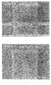
【表1】

結晶化した半導体層の状態は、走査型電子顕微鏡(SEM:Scanning Electron microscopy)で観察した。図32(A)はW1=8μm、W2=1μm、Δ=2μmとした試料のSEM像を示している。尚、試料は結晶粒を顕在化させるために、セコ液(主成分(体積比)HF:H2O=67:33、添加剤K2Cr2O7)で表面をエッチング処理してある。結晶は、図31において矢印で示したように、第1の絶縁層で形成される段差部からと、島状半導体層の端部から内側に向かって成長している様子がわかる。
【0154】
図32(B)は同試料において、第1の絶縁層が周期的に形成されない島状半導体層の端部の様子を観察したものである。その場合には、島状半導体層の内側部分に小さな結晶粒が集合した領域が観測されている。このような現象は本発明で述べる結晶化の機構を裏付けるものであり、島状半導体層の第1の絶縁層と重なる領域から結晶粒が成長することを示している。従って、W1とΔの大きさには最適な範囲があり、種々の形状の試料を作製して同様な評価を行った結果、表1で太線で囲んだ領域(W1は4〜10μm程度、Δは2〜5μm程度)で結晶粒の大粒径化を実現することができた。一方、W2は1μm程度が良好であり、それ以上大きくしていくと、第1の絶縁層上で別なモードの結晶成長が観測された。
【0155】
以上の実験結は、短冊状に形成する第1の絶縁層の間隔と、島状半導体層の幅を適した組合せで形成することにより、TFTのチャネル形成領域に合わせて大粒径の結晶質半導体層を形成できることを実証している。
【0156】
【発明の効果】
本発明のデュアルビームレーザーアニール法の技術を用いることにより、結晶粒の位置とその大きさを制御した結晶質半導体膜を作製することができる。このような結晶質半導体膜の結晶粒の位置をTFTのチャネル形成領域に合わせて形成することにより、TFTの静特性及び動特性を飛躍的に向上させることができる。
【図面の簡単な説明】
【図1】 本発明のデュアルビームレーザーアニール法の一例を説明する図。
【図2】 レーザーアニール装置の構成を説明する図。
【図3】 レーザーアニール装置の光学系の構成を説明する図
【図4】 レーザーアニール装置の光学系の構成を説明する図
【図5】 本発明の結晶化の工程を説明する図。
【図6】 本発明の結晶化の工程を説明する図。
【図7】 画素TFT、駆動回路のTFTの作製工程を示す断面図。
【図8】 画素TFT、駆動回路のTFTの作製工程を示す断面図。
【図9】 画素TFT、駆動回路のTFTの作製工程を示す断面図。
【図10】 画素TFT、駆動回路のTFTの作製工程を示す断面図。
【図11】 画素TFT、駆動回路のTFTの作製工程を示す断面図。
【図12】 駆動回路のTFTの作製工程を示す上面図。
【図13】 画素TFTの作製工程を示す上面図。
【図14】 駆動回路のTFTの作製工程を示す断面図。
【図15】 画素TFTの作製工程を示す断面図。
【図16】 アクティブマトリクス型液晶表示装置の断面図。
【図17】 液晶表示装置の構造を示す斜視図。
【図18】 画素部の画素構造を示す上面図。
【図19】 液晶表示装置の入出力端子、配線、回路配置、スペーサ、シール剤の配置を説明する上面図。
【図20】 EL表示装置の構造を示す上面図及び断面図。
【図21】 EL表示装置の画素部の断面図。
【図22】 EL表示装置の画素部の上面図と回路図。
【図23】 EL表示装置の画素部の断面図。
【図24】 EL表示装置の画素部の回路図の例。
【図25】 反強誘電性混合液晶の光透過率特性の一例を示す図。
【図26】 本発明の結晶化の工程を説明する図。
【図27】 本発明の結晶化の工程を説明する図。
【図28】 半導体装置の一例を示す図。
【図29】 半導体装置の一例を示す図。
【図30】 投影型液晶表示装置の構成を示す図。
【図31】 第1の絶縁層と島状半導体層を重ね合わせるときの寸法関係を説明する図。
【図32】 本発明により作製された結晶質半導体膜のSEM像。[0001]
BACKGROUND OF THE INVENTION
The present invention relates to a method for manufacturing a semiconductor film having a crystal structure formed over a substrate having an insulating surface, and a method for manufacturing a semiconductor device using the semiconductor film as an active layer. In particular, the present invention relates to a method for manufacturing a thin film transistor in which an active layer is formed using a crystalline semiconductor. Note that in this specification, a semiconductor device refers to all devices that can function by utilizing semiconductor characteristics, and an electro-optical device typified by an active matrix liquid crystal display device formed using thin film transistors, In addition, an electronic apparatus in which such an electro-optical device is mounted as a component is included in the category.
[0002]
[Prior art]
A thin film transistor is formed by forming an amorphous semiconductor film over a light-transmitting substrate having an insulating surface and crystallizing it by a heat treatment using a laser annealing method or a furnace annealing furnace (hereinafter referred to as a thermal annealing method). A technique for use in an active layer (Thin Film Transistor: hereinafter referred to as TFT) has been developed. As the light-transmitting substrate having an insulating surface, a glass substrate such as barium borosilicate glass or alumino borosilicate glass is often used. Although such a glass substrate is inferior in heat resistance to a quartz substrate, the commercial price is low, and there is an advantage that a large area substrate can be easily manufactured.
[0003]
The laser annealing method is known as a crystallization technique that does not raise the temperature of a glass substrate so much and can crystallize only an amorphous semiconductor film by applying high energy. In particular, an excimer laser that oscillates short-wavelength light having a wavelength of 400 nm or less is a typical laser that has been used since the development of this laser annealing method. In recent years, other technologies using a solid-state YAG laser have also been developed. In these laser annealing methods, a laser beam is processed by an optical system so as to be spot-like or linear on the irradiated surface, and the irradiated surface on the substrate is scanned with the processed laser light (laser light irradiation). The irradiation position is moved relative to the irradiated surface). For example, the excimer laser annealing method using linear laser light can also perform laser annealing of the entire irradiated surface by scanning only in the direction perpendicular to the longitudinal direction, and is excellent in productivity. It is becoming mainstream as a display device manufacturing technology. The technology enables a monolithic liquid crystal display device in which a TFT (pixel TFT) for forming a pixel portion on a single glass substrate and a TFT for a driving circuit provided around the pixel portion are formed.
[0004]
However, a crystalline semiconductor film produced by laser annealing an amorphous semiconductor film is a collection of a plurality of crystal grains, and the position and size of the crystal grains are random. A TFT manufactured on a glass substrate is formed by separating a crystalline semiconductor layer into an island pattern for element isolation. In that case, the position and size of the crystal grains could not be specified and formed. At the crystal grain interface (grain boundary), the current transport characteristics of the carrier deteriorate due to the influence of recombination centers, trap centers, and potential levels at the grain boundaries due to amorphous structures and crystal defects. It is known that there is. However, it has been almost impossible to form a channel formation region in which the properties of the crystal significantly affect the characteristics of the TFT with a single crystal grain by eliminating the influence of the grain boundary. For this reason, TFTs having a crystalline silicon film as an active layer have not been obtained to date with characteristics equivalent to those of MOS transistors fabricated on a single crystal silicon substrate.
[0005]
In order to solve such problems, attempts have been made to grow crystal grains greatly. For example, "" High-Mobility Poly-Si Thin-Film Transistors Fabricated by a Novel Excimer Laser Crystallization Method ", K. Shimizu, O. Sugiura and M. Matumura, IEEE Transactions on Electron Devices vol.40, No.1, pp112 -117,1993 "includes Si / SiO2 on the substrate. 2 There is a report on a laser annealing method in which a film having a three-layer structure of / Si is formed, and excimer laser light is irradiated from both the film side and the substrate side. According to the method, it is shown that the crystal grains can be enlarged by irradiating laser light with a certain predetermined energy intensity.
[0006]
[Problems to be solved by the invention]
The method of Ishihara et al. Is characterized in that the thermal characteristics of the underlying material of the amorphous silicon film are locally changed to control the flow of heat to the substrate so as to have a temperature gradient. However, for this purpose, a three-layer structure of a refractory metal layer / silicon oxide layer / semiconductor film is formed on a glass substrate. Although it is structurally possible to form a top gate TFT using this semiconductor film as an active layer, a parasitic capacitance is generated by the silicon oxide film provided between the semiconductor film and the refractory metal layer. As a result, power consumption increases and it is difficult to realize high-speed operation of the TFT.
[0007]
On the other hand, by using the refractory metal layer as a gate electrode, it is considered that the present invention can be effectively applied to a bottom gate type or an inverted stagger type TFT. However, in the three-layer structure, even if the thickness of the semiconductor film is excluded, the film thickness of the refractory metal layer and the silicon oxide layer is suitable for the film thickness suitable for the crystallization process and the characteristics as the TFT element. Since the film thickness does not always match, both the optimum design in the crystallization process and the optimum design of the element structure cannot be satisfied at the same time.
[0008]
Further, when a refractory metal layer having no translucency is formed on the entire surface of the glass substrate, it is impossible to manufacture a transmissive liquid crystal display device. Although the refractory metal layer is useful in terms of high thermal conductivity, the chromium (Cr) film and the titanium (Ti) film used as the refractory metal material have high internal stress, so the adhesion to the glass substrate There is a high possibility of problems. Further, the influence of the internal stress extends to the semiconductor film formed in the upper layer, and there is a high possibility that it acts as a force that distorts the formed crystalline semiconductor film.
[0009]
On the other hand, in order to control the threshold voltage (hereinafter referred to as Vth), which is an important characteristic parameter in the TFT, within a predetermined range, in addition to controlling the valence electrons in the channel formation region, It is necessary to reduce the charge defect density of the base film and the gate insulating film formed of the insulating film and to consider the balance of the internal stress. In response to such a requirement, a material containing silicon as a constituent element, such as a silicon oxide film or a silicon oxynitride film, was suitable. Therefore, there is a concern that the provision of the refractory metal layer to give a temperature gradient will break the balance.
[0010]
The present invention is a technique for solving such problems. A crystalline semiconductor film in which the position and size of crystal grains are controlled is produced, and the crystalline semiconductor film is used as a channel formation region of a TFT. As a result, a TFT capable of high-speed operation is realized. It is another object of the present invention to provide a technique in which such a TFT can be applied to various semiconductor devices such as a transmissive liquid crystal display device and a display device having an electroluminescent material.
[0011]
[Means for Solving the Problems]
Laser annealing is used as a method for forming a crystalline semiconductor layer from an amorphous semiconductor layer formed on a substrate such as glass. In the laser annealing method of the present invention, a pulse oscillation type or continuous light emission type excimer laser, YAG laser, or argon laser is used as a light source, and laser light formed in a linear or rectangular shape by an optical system is used as an island-shaped semiconductor layer. In contrast, the front side of the substrate on which the island-shaped semiconductor layer is formed (defined as a surface on which the island-shaped semiconductor layer is formed in this specification) and the back side (in this specification, the island-shaped semiconductor layer is formed). Irradiating from both the opposite surface and the opposite surface).
[0012]
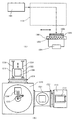
FIG. 2A is a diagram showing the configuration of the laser annealing apparatus of the present invention. The laser annealing apparatus includes a
[0013]
FIG. 3 is a view for explaining the basic configuration of the
[0014]
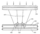
FIG. 1 is a diagram for explaining the concept of the laser annealing method of the present invention. A stripe-shaped or strip-shaped first insulating
[0015]
3A and 3B, the laser light that has passed through the
[0016]
In this way, laser light is irradiated from the front and back surfaces of the
[0017]
Irradiation with laser light from only one surface of the island-like semiconductor layer formed on the substrate heats only one side, so the cycle of heat melting and cooling solidification becomes steep, and the generation density of crystal nuclei Even if it can be controlled, sufficient crystal growth cannot be expected. However, when laser light is irradiated from both sides of the semiconductor layer, this heating and melting and cooling and solidification cycle becomes gradual, and the time allowed for crystal growth in the cooling and solidification process becomes relatively long. Crystal growth can be obtained.
[0018]
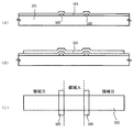
In the transient phenomenon, the island-like semiconductor layer is given a temperature distribution, a region where the temperature change is gentle is provided, and the nucleation rate and the nucleation density are controlled to increase the crystal grains. Specifically, as illustrated in FIG. 1, a stripe-shaped first insulating
[0019]
The method shown in FIG. 4 may be used as a method of irradiating laser light from the front surface side and the back surface side of the substrate in which the island-shaped semiconductor layer is formed on one surface. Light emitted from a
[0020]
In this specification, the laser annealing method having the configuration shown in FIGS. 1 and 4 is referred to as a dual beam laser annealing method, and the crystal grain size of the island-like semiconductor layer is increased by applying this method. By using the island-shaped semiconductor layer as an active layer of the TFT and further manufacturing a semiconductor device having a TFT having a structure corresponding to the function of each circuit, the performance of the semiconductor device is improved.
[0021]
Then, the configuration of the present invention using the dual beam laser annealing method includes a stripe-shaped first insulating layer on one surface of a light-transmitting substrate, and a second insulating layer on the stripe-shaped first insulating layer. Is provided. The island-shaped semiconductor layers provided on these insulating layers are formed so as to intersect with the stripe-shaped first insulating layers. As a preferred embodiment of the present invention, a plurality of stripe-shaped first insulating layers are formed, and an island-shaped semiconductor layer is formed so as to intersect with the plurality of stripe-shaped first insulating layers. A TFT channel formation region is formed between the single stripe-shaped first insulating layer and the adjacent stripe-shaped first insulating layer.
[0022]
As described above, the configuration of the present invention includes the island-shaped semiconductor layer and the strip-shaped first insulating layer provided below the island-shaped semiconductor layer on one surface of the light-transmitting substrate. The strip-shaped first insulating layer is provided so as to intersect with the island-shaped semiconductor layer. The first insulating layer may be formed in a pair, and the pair of strip-shaped first insulating layers are provided so as to intersect the island-shaped semiconductor layer.
[0023]
The above structure can be preferably applied to a TFT, and the channel formation region of the thin film transistor formed in the island-shaped semiconductor layer is formed adjacent to the strip-shaped first insulating layer, or the TFT A channel formation region is formed between a pair of strip-shaped first insulating layers.
[0024]
The method for manufacturing a semiconductor device according to the present invention includes a step of forming a strip-shaped first insulating layer on one surface of a light-transmitting substrate, and the strip-shaped first insulating layer on the strip-shaped first insulating layer. Irradiating the island-shaped semiconductor layer with laser light from the step of forming the island-shaped semiconductor layer so as to intersect the first insulating layer, and one surface side and the other surface side of the translucent substrate And the step of crystallizing the island-like semiconductor layer.
[0025]
In another aspect of the invention, a pair of strip-shaped first insulating layers is formed on one surface of a light-transmitting substrate, and the pair of strip-shaped first insulating layers is formed on the pair of strip-shaped first insulating layers. A laser is applied to the island-shaped semiconductor layer from the step of forming the island-shaped semiconductor layer so as to intersect the strip-shaped first insulating layer, and one surface side and the other surface side of the translucent substrate. And irradiating light to crystallize the island-shaped semiconductor layer.
[0026]
DETAILED DESCRIPTION OF THE INVENTION
[Embodiment 1]
An embodiment of the present invention will be described with reference to FIGS. In FIG. 5A, an alkali-free glass substrate such as barium borosilicate glass or alumino borosilicate glass is used for the
[0027]
Light-transmitting and insulating first insulating
[0028]
Any of the above oxides, nitrides, and compounds can be formed by sputtering or plasma CVD. In the case of sputtering, a target having a desired composition can be used, and sputtering can be performed using an inert gas such as argon (Ar) or nitrogen. Also, the thermal conductivity is 1000Wm -1 K -1 A thin-film diamond layer or a DLC (Diamond Like Carbon) layer that reaches the maximum thickness may be provided. In any case, by forming the first insulating
[0029]
Over this, a second insulating
[0030]
The island-shaped
[0031]
FIG. 6 is a diagram for explaining the crystallization process by the dual beam laser annealing method of the present invention. Crystallization uses a laser annealing method. In addition, a rapid thermal annealing method (RTA method) can also be applied. In the RTA method, an infrared lamp, a halogen lamp, a metal halide lamp, a xenon lamp, or the like is used as a light source. Also in this case, the light from the light source is irradiated from the substrate-side surface of the island-like semiconductor layer and the opposite surface. In the crystallization step, it is desirable to first release hydrogen contained in the amorphous semiconductor film, and heat treatment is performed at 400 to 500 ° C. for about 1 hour so that the amount of hydrogen contained is 5 atomic% or less. .
[0032]
When crystallization is performed by laser annealing, a pulse oscillation type or continuous emission type excimer laser, YAG laser, or argon laser is used as the light source. The structure of the laser annealing method is as shown in FIGS.
[0033]
FIG. 6A shows a state in which the
[0034]
In the structure of FIG. 6A, the volume where the first insulating
[0035]
As a result, large-grain crystals grow around the first insulating
[0036]
After that, the island-like semiconductor layer remains by heat treatment at 300 to 450 ° C. in an atmosphere containing 3 to 100% hydrogen, or heat treatment at 200 to 450 ° C. in an atmosphere containing hydrogen generated by plasma. Defects can be neutralized. By manufacturing the TFT active layer using the region A of the island-shaped
[0037]
[Embodiment 2]
The method for producing the island-shaped semiconductor layer having a crystal structure as the active layer of the TFT is not produced only by the laser annealing method, and the laser annealing method and the thermal annealing method according to the present invention may be used in combination. In particular, crystallization by thermal annealing can be realized at a temperature of 600 ° C. or lower when applied to the crystallization method using a catalytic element disclosed in Japanese Patent Application Laid-Open No. 7-130652. When the crystalline semiconductor layer is processed by the laser annealing method according to the present invention, a high-quality crystalline semiconductor layer can be obtained. Such an embodiment will be described with reference to FIG.
[0038]
In FIG. 26A, the glass substrate described in
[0039]
Thereafter, heat treatment is first performed at 400 to 500 ° C. for about 1 hour, so that the hydrogen content of the amorphous semiconductor layer is 5 atom% or less. Then, using a furnace annealing furnace, thermal annealing is performed in a nitrogen atmosphere at 550 to 600 ° C. for 1 to 8 hours, preferably at 550 ° C. for 4 hours. Through the above steps, a
[0040]
As shown in FIG. 26C, an island-shaped semiconductor layer is formed from the
[0041]
[Embodiment 3]
The method of crystallizing a semiconductor layer by the dual beam laser annealing method of the present invention is characterized in that a large crystal is grown in the region A as described with reference to FIGS. In this embodiment, another method for forming a similar crystalline semiconductor layer will be described.
[0042]
As shown in FIG. 27A, the glass substrate described in
[0043]
Thereafter, as shown in FIG. 27C, dual beam laser annealing is performed in the same manner as in the first embodiment. As a result, an island-shaped semiconductor layer 571 having a new crystal structure is formed once in a molten state by the
[0044]
【Example】
[Example 1]
An embodiment of the present invention will be described with reference to FIGS. Here, a process for simultaneously manufacturing an n-channel TFT (hereinafter referred to as a pixel TFT) and a storage capacitor in a pixel portion, and an n-channel TFT and a p-channel TFT in a driver circuit provided around the pixel portion are described. It explains according to.
[0045]
In FIG. 7A, a barium borosilicate glass substrate or an alumino borosilicate glass substrate is used as the
[0046]
In the case where a silicon oxide film is used, tetraethyl orthosilicate (TEOS) and O2 are formed by plasma CVD. 2 The reaction pressure is 40 Pa, the substrate temperature is 300 to 400 ° C., and the high frequency (13.56 MHz) power density is 0.5 to 0.8 W / cm. 2 And can be formed by discharging. When using a silicon oxynitride film, SiH is formed by plasma CVD. Four , N 2 O, NH Three Silicon oxynitride film manufactured from SiH or SiH Four , N 2 A silicon oxynitride film formed from O may be used. The production conditions in this case are a reaction pressure of 20 to 200 Pa, a substrate temperature of 300 to 400 ° C., and a high frequency (60 MHz) power density of 0.1 to 1.0 W / cm. 2 Can be formed. SiH Four , N 2 O, H 2 Alternatively, a silicon oxynitride silicon film manufactured from the above may be used. Similarly, the silicon nitride film is made of SiH by plasma CVD. Four , NH Three It is possible to make from.
[0047]
As the first insulating layer, an insulating film typified above is formed on the entire surface of the
[0048]
The pattern size of the first insulating layer is appropriately determined by the practitioner, but in actuality, it may be determined in consideration of the size (channel length, channel width) of the TFT to be manufactured. For example, 0.5 to 2 μm (preferably 1 μm) with respect to the channel length direction of the TFT forming the first insulating
[0049]
Next, a second insulating
[0050]
Next, a semiconductor layer 208 having an amorphous structure with a thickness of 25 to 80 nm (preferably 30 to 60 nm) is formed by a known method such as a plasma CVD method or a sputtering method. In this embodiment, an amorphous silicon film is formed to a thickness of 55 nm by plasma CVD. As the semiconductor film having an amorphous structure, there are an amorphous semiconductor film and a microcrystalline semiconductor film, and a compound semiconductor film having an amorphous structure such as an amorphous silicon germanium film may be applied. In addition, since the second insulating
[0051]
Then, as shown in FIG. 7B, unnecessary portions of the amorphous semiconductor layer 208 are removed by etching to form island-shaped semiconductor layers 209 to 212. The practitioner may determine the shape and size of the island-shaped semiconductor layer as appropriate. For example, when combined with the first insulating
[0052]
The island-shaped semiconductor layers 209 to 212 are crystallized by a dual beam laser annealing method. Any of the methods shown in the first to third embodiments may be applied. For example, a XeCl excimer laser (wavelength 308 nm) is used as a laser beam generator, the laser annealing apparatus shown in FIGS. 2 to 4 is used to form a linear beam with an optical system, an oscillation frequency of 5 to 50 Hz, and an energy density of 100 to 500mJ / cm 2 Irradiation is performed with a linear beam overlap ratio of 80 to 98%. In this way, the island-shaped semiconductor layers 209 to 212 are crystallized.
[0053]
Thereafter, a
[0054]
In the channel doping process, a
[0055]
Then, in order to form an LDD region of the n-channel TFT of the driver circuit, an impurity element imparting n-type conductivity is selectively added to the island-shaped semiconductor layers 210b and 211b. Photoresist masks 215 to 218 are formed in advance. In this process, phosphine (PH) is added to add phosphorus (P). Three The ion doping method using) is applied. Impurity region (n - ) The phosphorus (P) concentration of 219, 220 is 1 × 10 17 ~ 5x10 19 atoms / cm Three (FIG. 8A). The
[0056]
Next, the
[0057]
Then, the
[0058]
Next, a first conductive layer for forming a gate electrode is formed. Although this conductive layer may be formed as a single layer, it may have a laminated structure of two layers or three layers as required. In this embodiment, a conductive layer (A) 223 made of a conductive nitride metal film and a conductive layer (B) 224 made of a metal film are stacked. The conductive layer (B) 224 is an element selected from tantalum (Ta), titanium (Ti), molybdenum (Mo), and tungsten (W), an alloy containing the element as a main component, or an alloy film in which the elements are combined. (Typically, the conductive layer (A) 223 may be formed of tantalum nitride (TaN), tungsten nitride (WN), titanium nitride (TiN) film, or nitride). It is made of molybdenum (MoN) or the like. Alternatively, tungsten silicide, titanium silicide, or molybdenum silicide may be used for the conductive layer (A) 223. In the conductive layer (B) 224, the concentration of impurities contained in the conductive layer (B) 224 is preferably reduced in order to reduce the resistance. For example, tungsten (W) can realize a specific resistance value of 20 μΩcm or less by setting the oxygen concentration to 30 ppm or less.
[0059]
The conductive layer (A) 223 may be 10 to 50 nm (preferably 20 to 30 nm), and the conductive layer (B) 224 may be 200 to 400 nm (preferably 250 to 350 nm). In this embodiment, a 30 nm thick TaN film is used for the conductive layer (A) 223 and a 350 nm Ta film is used for the conductive layer (B) 224, both of which are formed by sputtering. The TaN film is formed by using Ta as a target and using a mixed gas of Ar and nitrogen as a sputtering gas. Ta uses Ar as the sputtering gas. In addition, when an appropriate amount of Xe or Kr is added to these sputtering gases, the internal stress of the film to be formed can be relaxed and the film can be prevented from peeling. The resistivity of the α-phase Ta film is about 20 μΩcm and can be used as a gate electrode, but the resistivity of the β-phase Ta film is about 180 μΩcm and is not suitable for a gate electrode. Since the TaN film has a crystal structure close to an α phase, an α phase Ta film can be easily obtained by forming a Ta film thereon. Although not shown, it is effective to form a silicon film doped with phosphorus (P) with a thickness of about 2 to 20 nm under the conductive layer (A) 223. This improves adhesion and prevents oxidation of the conductive film formed thereon, and at the same time, an alkali metal element contained in a trace amount in the conductive layer (A) or the conductive layer (B) diffuses into the
[0060]
Next, photoresist masks 225 to 229 are formed, and the conductive layer (A) 223 and the conductive layer (B) 224 are collectively etched to form
[0061]
Next, in order to form a source region and a drain region of the p-channel TFT of the driver circuit, a step of adding an impurity element imparting p-type is performed. Here, the impurity region is formed in a self-aligning manner using the
[0062]
Next, in the n-channel TFT, an impurity region functioning as a source region or a drain region is formed. Resist masks 237 to 239 are formed, and an impurity element imparting n-type conductivity is added to form impurity regions 241 to 244. This is the phosphine (PH Three The impurity region (n + ) (P) concentration of 241 to 244 is 5 × 10 20 atoms / cm Three (FIG. 9B). The
[0063]
Then, in order to form an LDD region of the n-channel TFT in the pixel portion, an impurity addition step for imparting n-type is performed. Here, an impurity element imparting n-type is added by ion doping in a self-aligning manner using the
[0064]
Thereafter, a heat treatment process is performed to activate the impurity element imparting n-type or p-type added at each concentration. This step can be performed by a thermal annealing method using a furnace annealing furnace, a laser annealing method, or a rapid thermal annealing method (RTA method). Here, the activation process is performed by furnace annealing. The heat treatment is performed at 400 to 700 ° C., typically 500 to 600 ° C. in a nitrogen atmosphere having an oxygen concentration of 1 ppm or less, preferably 0.1 ppm or less. In this embodiment, the heat treatment is performed at 550 ° C. for 4 hours. Do.
[0065]
In the thermal annealing, conductive films (C) 230c to 234c made of TaN are formed with a thickness of 5 to 80 nm from the surface of the Ta films 230b to 234b formed on the
[0066]
When a catalytic element that promotes crystallization of silicon is used in the crystallization process, and then the gettering process described in
[0067]
12A and 13A are top views of the TFT in FIG. 9D, and the AA ′ cross section and the CC ′ cross section are AA ′ and C in FIG. 9D. Corresponds to -C '. The BB ′ cross section and the DD ′ cross section correspond to the cross sectional views of FIGS. 14A and 15A. Although the gate insulating film is omitted in the top views of FIGS. 12 and 13, the gates are formed on the island-shaped semiconductor layers 209, 210, and 212 formed on the first and second insulating layers in the steps so far.
[0068]
When the activation and hydrogenation steps are completed, a second conductive layer for forming a gate line is formed. The second conductive layer is formed of a conductive layer (D) mainly composed of aluminum (Al) or copper (Cu) which is a low resistance material. In any case, the resistivity of the second conductive layer is about 0.1 to 10 μΩcm. Further, a conductive layer (E) made of titanium (Ti), tantalum (Ta), tungsten (W), or molybdenum (Mo) is preferably stacked. In this example, the conductive layer (D) 247 was formed using an aluminum (Al) film containing 0.1 to 2 wt% of titanium (Ti), and the titanium (Ti) film was formed as the conductive layer (E) 248. The conductive layer (D) 247 may be 200 to 400 nm (preferably 250 to 350 nm), and the conductive layer (E) 248 may be formed of 50 to 200 (preferably 100 to 150 nm) (FIG. 10A). ).
[0069]
Then, in order to form a gate line connected to the gate electrode, the conductive layer (E) 248 and the conductive layer (D) 247 are etched to form
[0070]
12B and 13B are top views of this state, and the AA ′ and CC ′ sections correspond to AA ′ and CC ′ in FIG. 10B. ing. Further, the BB ′ cross section and the DD ′ cross section correspond to BB ′ and DD ′ in FIGS. 14B and 15B. 12B and 13B, part of the
[0071]
The first
[0072]
Next, a silicon nitride film, a silicon oxide film, or a silicon oxynitride film is formed as the
[0073]
FIGS. 12C and 13C are top views of this state, and the AA ′ and CC ′ sections correspond to AA ′ and CC ′ in FIG. 10C. is doing. Further, the BB ′ section and the DD ′ section correspond to BB ′ and DD ′ in FIGS. 14C and 15C. Although the first interlayer insulating film is omitted in FIGS. 12C and 13C, source lines 253, 254, and the like are not shown in the source and drain regions of the island-shaped semiconductor layers 209, 210, and 212. 256 and
[0074]
Thereafter, as shown in FIG. 11, a second
[0075]
In this manner, a substrate having the TFT of the driving circuit and the pixel TFT of the pixel portion can be completed on the same substrate. A p-
[0076]
The p-
[0077]
The configuration as described above makes it possible to optimize the structure of the TFT constituting each circuit according to the specifications required by the pixel TFT and the drive circuit, and to improve the operation performance and reliability of the semiconductor device. Furthermore, the LDD region, the source region, and the drain region can be easily activated by forming the gate electrode from a heat-resistant conductive material, and the wiring resistance can be sufficiently reduced by forming the gate electrode from a low-resistance material. Therefore, the present invention can be applied to a display device having a pixel portion (screen size) of 4 inch class or more. Then, by using a crystalline silicon film having a single crystal structure which is selectively formed over the first insulating
[0078]
[Example 2]
In this embodiment, a process of manufacturing an active matrix liquid crystal display device from the active matrix substrate manufactured in
[0079]
Next, the configuration of the active matrix liquid crystal display device will be described with reference to the perspective view of FIG. 17 and the top view of FIG. Note that FIGS. 17 and 18 use common reference numerals in order to correspond to the cross-sectional structure diagrams of FIGS. 7 to 11 and FIG. 16. Further, the cross-sectional structure along the line EE ′ shown in FIG. 18 corresponds to the cross-sectional view of the pixel matrix circuit shown in FIG.
[0080]
In FIG. 17, the active matrix substrate includes a
[0081]
FIG. 18 is a top view showing almost one pixel of the
[0082]
Note that the active matrix liquid crystal display device of this example has been described with reference to the structure described in Example 1, but is not limited to the configuration of Example 1, and is described in
[0083]
[Example 3]
FIG. 19 is a diagram illustrating an example of an arrangement of input / output terminals, a pixel portion, and a driving circuit of a liquid crystal display device. In the
[0084]
A scanning
[0085]
On the other hand, when the screen size of the pixel portion is 0.9 inch class, the length of the diagonal line is about 24 mm, and when the TFT is manufactured according to the submicron rule, the driving circuit provided in the periphery is 30 × 30 mm. 2 Fits within. In such a case, it is not always necessary to form the gate wiring with the low resistance material as shown in the
[0086]
The liquid crystal display device having such a structure can be completed using an active matrix substrate that is completed by applying the crystallization method shown in
[0087]
[Example 4]
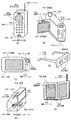
In this embodiment, an example in which an EL (electroluminescence) display device is manufactured using the active matrix substrate of the present invention will be described. FIG. 20A is a top view of an EL display device using the present invention. In FIG. 20A, 10 is a substrate, 11 is a pixel portion, 12 is a source side driver circuit, 13 is a gate side driver circuit, and each driver circuit reaches the
[0088]
At this time, the
[0089]
FIG. 20B shows a cross-sectional structure of the EL display device of this embodiment. A driving circuit TFT (here, an n-channel TFT and a p-channel TFT are combined on the
[0090]
When the
[0091]
Next, the
[0092]
In this embodiment, the EL layer is formed by vapor deposition using a shadow mask. Color display is possible by forming a light emitting layer (a red light emitting layer, a green light emitting layer, and a blue light emitting layer) capable of emitting light having different wavelengths for each pixel using a shadow mask. In addition, there are a method in which a color conversion layer (CCM) and a color filter are combined, and a method in which a white light emitting layer and a color filter are combined, but either method may be used. Needless to say, an EL display device emitting monochromatic light can also be used.
[0093]
After the
[0094]
In this embodiment, a laminated structure of a LiF (lithium fluoride) film and an Al (aluminum) film is used as the
[0095]
In order to electrically connect the
[0096]
Further, the
[0097]
The present invention can be used in an EL display device having the above structure. Here, a more detailed cross-sectional structure of the pixel portion is shown in FIG. 21, a top structure is shown in FIG. 22A, and a circuit diagram is shown in FIG. 22B. In FIG. 21, FIG. 22 (A), and FIG.
[0098]
In FIG. 21, a switching
[0099]
The
[0100]
At this time, it is very important that the
[0101]
In this embodiment, the
[0102]
As shown in FIG. 22A, the wiring that becomes the
[0103]
A
[0104]
[0105]
A
[0106]
There are various types of PPV organic EL materials. For example, “H. Shenk, Becker, O. Gelsen, E. Kluge, W. Kreuder and H. Spreitzer,“ Polymers for Light Emitting Diodes ” , Euro Display, Proceedings, 1999, p. 33-37 "or JP-A-10-92576.
[0107]
As a specific light emitting layer, cyanopolyphenylene vinylene may be used for a light emitting layer that emits red light, polyphenylene vinylene may be used for a light emitting layer that emits green light, and polyphenylene vinylene or polyalkylphenylene may be used for a light emitting layer that emits blue light. The film thickness may be 30 to 150 nm (preferably 40 to 100 nm).
[0108]
However, the above example is an example of an organic EL material that can be used as a light emitting layer, and is not necessarily limited to this. An EL layer (a layer for emitting light and moving carriers therefor) may be formed by freely combining a light-emitting layer, a charge transport layer, or a charge injection layer.
[0109]
For example, in this embodiment, an example in which a polymer material is used as the light emitting layer is shown, but a low molecular weight organic EL material may be used. It is also possible to use an inorganic material such as silicon carbide for the charge transport layer or the charge injection layer. As these organic EL materials and inorganic materials, known materials can be used.
[0110]
In this embodiment, the EL layer has a laminated structure in which a
[0111]
When the
[0112]
By the way, in the present embodiment, a
[0113]
As described above, the EL display device of the present invention has a pixel portion composed of pixels having a structure as shown in FIG. 21, and includes a switching TFT having a sufficiently low off-current value and a current control TFT resistant to hot carrier injection. Have. Therefore, an EL display device having high reliability and capable of displaying a good image can be obtained.
[0114]
In addition, the structure of a present Example can be freely combined with the structure of Embodiment 1-3 and Example 1, and can be implemented. Further, it is effective to use the EL display device of this embodiment as the display unit of the electronic apparatus of
[0115]
[Example 5]
In this embodiment, a structure in which the structure of the
[0116]
In FIG. 23, a current control TFT 2601 is formed using the p-channel TFT of the present invention. For the manufacturing process, Example 1 may be referred to. In this embodiment, a transparent conductive film is used as the pixel electrode (anode) 50. Specifically, a conductive film made of a compound of indium oxide and zinc oxide is used. Of course, a conductive film made of a compound of indium oxide and tin oxide may be used.
[0117]
Then, after
[0118]
In the case of the present embodiment, the light generated in the
[0119]
In addition, the structure of a present Example can be freely combined with the structure of Embodiment 1-3 and Example 1, and can be implemented. Further, it is effective to use the EL display of this embodiment as the display unit of the electronic apparatus of
[0120]
[Example 6]
In this embodiment, an example of a pixel having a structure different from the circuit diagram shown in FIG. 22B is shown in FIG. In this embodiment, 2701 is a source wiring of the switching
[0121]
FIG. 24A shows an example in which the
[0122]
FIG. 24B illustrates an example in which the
[0123]
In FIG. 24C, a
[0124]
In FIGS. 24A and 24B, a
[0125]
Since the n-channel TFT of the present invention as shown in FIG. 21 is used as the
[0126]
Since the capacitance of the parasitic capacitance varies depending on the area where the gate electrode and the LDD region overlap, it is determined by the length of the LDD region included in the overlapping region.
[0127]
Similarly, the
[0128]
In addition, the structure of a present Example can be freely combined with the structure of Embodiment 1-3 and Example 1, and can be implemented. In addition, it is effective to use the EL display device having the pixel structure of this embodiment as the display unit of the electronic apparatus of
[0129]
[Example 7]
In addition to nematic liquid crystals, various liquid crystals can be used for the liquid crystal display device shown in
[0130]
Ferroelectric liquid crystal (FLC) exhibiting an isotropic phase-cholesteric phase-chiral smectic phase transition series is used to cause a cholesteric phase-chiral smectic phase transition while applying a DC voltage, and to make the cone edge substantially coincide with the rubbing direction. The electro-optical characteristics of the monostable FLC are shown in FIG. The display mode using the ferroelectric liquid crystal as shown in FIG. 25 is called “Half-V-shaped switching mode”. The vertical axis of the graph shown in FIG. 25 is the transmittance (arbitrary unit), and the horizontal axis is the applied voltage. Regarding “Half-V-shaped switching mode”, Terada et al., “Half-V-shaped switching mode FLCD”, Proceedings of the 46th Joint Physics Related Conference, March 1999, p. 1316, and Yoshihara et al. "Time-division full-color LCD using ferroelectric liquid crystal", Liquid Crystal, Vol. 3, No. 3, page 190.
[0131]
As shown in FIG. 25, it can be seen that when such a ferroelectric mixed liquid crystal is used, low voltage driving and gradation display are possible. In the liquid crystal display device of the present invention, a ferroelectric liquid crystal exhibiting such electro-optical characteristics can also be used.
[0132]
A liquid crystal exhibiting an antiferroelectric phase in a certain temperature range is called an antiferroelectric liquid crystal (AFLC). Among mixed liquid crystals having antiferroelectric liquid crystals, there is a so-called thresholdless antiferroelectric mixed liquid crystal that exhibits electro-optic response characteristics in which transmittance continuously changes with respect to an electric field. This thresholdless antiferroelectric mixed liquid crystal has a so-called V-shaped electro-optic response characteristic, and a drive voltage of about ± 2.5 V (cell thickness of about 1 μm to 2 μm) is also found. Has been.
[0133]
In general, the thresholdless antiferroelectric mixed liquid crystal has a large spontaneous polarization, and the dielectric constant of the liquid crystal itself is high. For this reason, when a thresholdless antiferroelectric mixed liquid crystal is used in a liquid crystal display device, a relatively large storage capacitor is required for the pixel. Therefore, it is preferable to use a thresholdless antiferroelectric mixed liquid crystal having a small spontaneous polarization.
[0134]
In addition, since such a thresholdless antiferroelectric mixed liquid crystal is used for the liquid crystal display device of the present invention, low voltage driving is realized, so that low power consumption is realized.
[0135]
[Example 8]
In this embodiment, a semiconductor device incorporating an active matrix liquid crystal display device using a TFT circuit of the present invention will be described with reference to FIGS.
[0136]
Examples of such a semiconductor device include a portable information terminal (electronic notebook, mobile computer, mobile phone, etc.), a video camera, a still camera, a personal computer, a television, and the like. Examples of these are shown in FIGS.
[0137]
FIG. 28A illustrates a mobile phone, which includes a main body 9001, an
[0138]
FIG. 28B illustrates a video camera which includes a main body 9101, a display device 9102, an
[0139]
FIG. 28C illustrates a mobile computer, which includes a main body 9201, a camera portion 9202, an image receiving portion 9203, operation switches 9204, and a display device 9205. The present invention can be applied to the image receiving portion 9203 and a display device 9205 including an active matrix substrate.
[0140]
FIG. 28D illustrates a head mounted display which includes a main body 9301, a
[0141]
FIG. 28E shows a rear projector, which includes a main body 9401, a light source 9402, a
[0142]
FIG. 28F illustrates a portable book which includes a main body 9501,
[0143]
FIG. 29A illustrates a personal computer which includes a main body 9601, an
[0144]
FIG. 29B shows a player using a recording medium (hereinafter referred to as a recording medium) in which a program is recorded, and includes a main body 9701, a
[0145]
FIG. 29C illustrates a digital camera, which includes a main body 9801, a
[0146]
FIG. 30A illustrates a front type projector which includes a
[0147]
FIG. 30B illustrates a rear projector, which includes a main body 3701, a
[0148]
Note that FIG. 30C illustrates an example of a structure of the
[0149]
FIG. 30D is a diagram illustrating an example of the structure of the light source optical system 3801 in FIG. In this embodiment, the light source optical system 3801 includes a reflector 3811, a light source 3812,
[0150]
The present invention can also be applied to image sensors and EL display elements. As described above, the scope of application of the present invention is extremely wide and can be applied to electronic devices in various fields.
[0151]
[Example 9]
A combination that can increase the size of crystal grains by changing the width of the first insulating layer and the width of the island-shaped semiconductor layer that intersects the width of the first insulating layer was studied. As shown in FIG. 31, W1 is 4 to 50 μm and W2 as shown in Table 1, where W2 is the width of the first insulating layer formed in a strip shape as shown in FIG. In the range of 1 to 5 μm and Δ in the range of 2 to 10 μm. The first insulating layer was formed with a thickness of 30 nm, the second insulating layer formed over the first insulating layer was formed with a thickness of 160 nm, and the island-shaped semiconductor layer was formed with a thickness of 55 nm. Crystallization was performed by irradiating with an energy of 460 mJ / cm @ 2 using a dual beam laser annealing method.
[0152]
[Table 1]
The state of the crystallized semiconductor layer was observed with a scanning electron microscope (SEM). FIG. 32A shows an SEM image of a sample with W1 = 8 μm, W2 = 1 μm, and Δ = 2 μm. In addition, in order to reveal crystal grains, the sample is a Seco liquid (main component (volume ratio) HF: H 2 O = 67: 33, additive K 2 Cr 2 O 7 The surface is etched with As shown by arrows in FIG. 31, it can be seen that the crystal grows inward from the stepped portion formed of the first insulating layer and from the end of the island-shaped semiconductor layer.
[0154]
FIG. 32B shows the state of the end portion of the island-shaped semiconductor layer in which the first insulating layer is not periodically formed in the sample. In that case, a region where small crystal grains are gathered in the inner part of the island-like semiconductor layer is observed. Such a phenomenon supports the crystallization mechanism described in the present invention, and indicates that crystal grains grow from a region of the island-shaped semiconductor layer overlapping the first insulating layer. Therefore, there is an optimum range for the sizes of W1 and Δ, and as a result of producing samples having various shapes and performing similar evaluation, the region surrounded by the thick line in Table 1 (W1 is about 4 to 10 μm, Δ Was about 2 to 5 μm), and a large grain size could be realized. On the other hand, W2 is preferably about 1 μm, and when it is further increased, another mode of crystal growth was observed on the first insulating layer.
[0155]
The above experimental results show that the crystalline structure having a large grain size according to the channel formation region of the TFT is formed by forming the gap between the first insulating layers formed in a strip shape and the width of the island-like semiconductor layer in an appropriate combination. It has been demonstrated that a semiconductor layer can be formed.
[0156]
【The invention's effect】
By using the technique of the dual beam laser annealing method of the present invention, a crystalline semiconductor film in which the position and size of crystal grains are controlled can be manufactured. By forming the crystal grain position of such a crystalline semiconductor film in accordance with the channel formation region of the TFT, the static characteristics and dynamic characteristics of the TFT can be dramatically improved.
[Brief description of the drawings]
FIG. 1 illustrates an example of a dual beam laser annealing method of the present invention.
FIG. 2 is a diagram illustrating a configuration of a laser annealing apparatus.
FIG. 3 is a diagram for explaining the configuration of an optical system of a laser annealing apparatus.
FIG. 4 is a diagram for explaining the configuration of an optical system of a laser annealing apparatus.
FIG. 5 is a diagram illustrating a crystallization process of the present invention.
FIG. 6 is a diagram illustrating a crystallization process of the present invention.
FIG. 7 is a cross-sectional view illustrating a manufacturing process of a pixel TFT and a TFT of a driver circuit.
FIG. 8 is a cross-sectional view illustrating a manufacturing process of a pixel TFT and a TFT of a driver circuit.
FIG. 9 is a cross-sectional view illustrating a manufacturing process of a pixel TFT and a driver circuit TFT;
FIG. 10 is a cross-sectional view illustrating a manufacturing process of a pixel TFT and a TFT of a driver circuit.
FIG. 11 is a cross-sectional view illustrating a manufacturing process of a pixel TFT and a TFT of a driver circuit.
FIG. 12 is a top view illustrating a manufacturing process of a TFT of a driver circuit.
FIG. 13 is a top view illustrating a manufacturing process of a pixel TFT.
FIG. 14 is a cross-sectional view showing a manufacturing process of a TFT of a driver circuit.
FIG. 15 is a cross-sectional view illustrating a manufacturing process of a pixel TFT.
FIG. 16 is a cross-sectional view of an active matrix liquid crystal display device.
FIG. 17 is a perspective view illustrating a structure of a liquid crystal display device.
FIG. 18 is a top view illustrating a pixel structure of a pixel portion.
FIG. 19 is a top view illustrating an arrangement of input / output terminals, wiring, circuit arrangement, spacers, and a sealant of a liquid crystal display device.
20A and 20B are a top view and a cross-sectional view illustrating a structure of an EL display device.
FIG. 21 is a cross-sectional view of a pixel portion of an EL display device.
FIGS. 22A and 22B are a top view and a circuit diagram of a pixel portion of an EL display device. FIGS.
FIG. 23 is a cross-sectional view of a pixel portion of an EL display device.
FIG. 24 is an example of a circuit diagram of a pixel portion of an EL display device.
FIG. 25 is a diagram showing an example of light transmittance characteristics of an antiferroelectric mixed liquid crystal.
FIG 26 illustrates a crystallization process of the present invention.
FIG. 27 is a diagram illustrating a crystallization process of the present invention.
FIG 28 illustrates an example of a semiconductor device.
FIG 29 illustrates an example of a semiconductor device.
FIG. 30 is a diagram showing a configuration of a projection type liquid crystal display device.
FIG. 31 illustrates a dimensional relationship when a first insulating layer and an island-shaped semiconductor layer are overlaid.
FIG. 32 is an SEM image of a crystalline semiconductor film manufactured according to the present invention.
Claims (9)
前記短冊状の絶縁層上に、前記短冊状の絶縁層と交差するように島状半導体層を形成し、
前記透光性基板の表面側と、裏面側とから、前記島状半導体層にレーザー光を照射して、前記島状半導体層を結晶化することを特徴とする半導体装置の作製方法。A strip-shaped insulating layer is formed on the surface of the translucent substrate,
On the strip-shaped insulating layer, an island-shaped semiconductor layer is formed so as to intersect with the strip-shaped insulating layer,
A method for manufacturing a semiconductor device, wherein the island-shaped semiconductor layer is crystallized by irradiating the island-shaped semiconductor layer with laser light from a front surface side and a back surface side of the translucent substrate.
前記一対の短冊状の絶縁層上に、前記一対の短冊状の絶縁層と交差するように島状半導体層を形成し、
前記透光性基板の表面側と、裏面側とから、前記島状半導体層にレーザー光を照射して、前記島状半導体層を結晶化することを特徴とする半導体装置の作製方法。Forming a pair of strip-like insulating layers on the surface of the light-transmitting substrate;
On the pair of strip-shaped insulating layers, an island-shaped semiconductor layer is formed so as to intersect the pair of strip-shaped insulating layers,
A method for manufacturing a semiconductor device, wherein the island-shaped semiconductor layer is crystallized by irradiating the island-shaped semiconductor layer with laser light from a front surface side and a back surface side of the translucent substrate.
透光性基板の表面に短冊状の絶縁層を形成し、
前記短冊状の絶縁層上に、前記短冊状の絶縁層と交差するように前記薄膜トランジスタとなる島状半導体層を形成し、
前記透光性基板の表面側と、裏面側とから、前記島状半導体層にレーザー光を照射して、前記島状半導体層を結晶化することを特徴とする半導体装置の作製方法。In a method for manufacturing a semiconductor device having a thin film transistor,
A strip-shaped insulating layer is formed on the surface of the translucent substrate,
On the strip-shaped insulating layer, an island-shaped semiconductor layer to be the thin film transistor is formed so as to intersect the strip-shaped insulating layer,
A method for manufacturing a semiconductor device, wherein the island-shaped semiconductor layer is crystallized by irradiating the island-shaped semiconductor layer with laser light from a front surface side and a back surface side of the translucent substrate.
透光性基板の表面に一対の短冊状の絶縁層を形成し、
前記一対の短冊状の絶縁層上に、前記一対の短冊状の絶縁層と交差するように前記薄膜トランジスタとなる島状半導体層を形成し、
前記透光性基板の表面側と、裏面側とから、前記島状半導体層にレーザー光を照射して、前記島状半導体層を結晶化することを特徴とする半導体装置の作製方法。In a method for manufacturing a semiconductor device having a thin film transistor,
Forming a pair of strip-like insulating layers on the surface of the light-transmitting substrate;
On the pair of strip-shaped insulating layers, an island-shaped semiconductor layer to be the thin film transistor is formed so as to intersect the pair of strip-shaped insulating layers,
A method for manufacturing a semiconductor device, wherein the island-shaped semiconductor layer is crystallized by irradiating the island-shaped semiconductor layer with laser light from a front surface side and a back surface side of the translucent substrate.
透光性基板の表面に短冊状の絶縁層を形成し、
前記短冊状の絶縁層上に、前記短冊状の絶縁層とチャネル長方向が交差するように、前記薄膜トランジスタとなる島状半導体層を形成し、
前記透光性基板の表面側と、裏面側とから、前記島状半導体層にレーザー光を照射して、前記島状半導体層を結晶化することを特徴とする半導体装置の作製方法。In a method for manufacturing a semiconductor device having a thin film transistor,
A strip-shaped insulating layer is formed on the surface of the translucent substrate,
On the strip-shaped insulating layer, an island-shaped semiconductor layer to be the thin film transistor is formed so that the strip-shaped insulating layer and the channel length direction intersect,
A method for manufacturing a semiconductor device, wherein the island-shaped semiconductor layer is crystallized by irradiating the island-shaped semiconductor layer with laser light from a front surface side and a back surface side of the translucent substrate.
透光性基板の表面に一対の短冊状の絶縁層を形成し、
前記一対の短冊状の絶縁層上に、前記一対の短冊状の絶縁層とチャネル長方向が交差するように、前記薄膜トランジスタとなる島状半導体層を形成し、
前記透光性基板の表面側と、裏面側とから、前記島状半導体層にレーザー光を照射して、前記島状半導体層を結晶化することを特徴とする半導体装置の作製方法。In a method for manufacturing a semiconductor device having a thin film transistor,
Forming a pair of strip-like insulating layers on the surface of the light-transmitting substrate;
On the pair of strip-shaped insulating layers, an island-shaped semiconductor layer to be the thin film transistor is formed so that the channel length direction intersects with the pair of strip-shaped insulating layers,
A method for manufacturing a semiconductor device, wherein the island-shaped semiconductor layer is crystallized by irradiating the island-shaped semiconductor layer with laser light from a front surface side and a back surface side of the translucent substrate.
前記短冊状の絶縁層を形成する工程と、前記島状半導体層を形成する工程との間に、絶縁層を形成する工程を有することを特徴とする半導体装置の作製方法。In any one of Claims 1 thru | or 6,
A method for manufacturing a semiconductor device, comprising a step of forming an insulating layer between the step of forming the strip-shaped insulating layer and the step of forming the island-shaped semiconductor layer.
前記透光性基板の裏面側から前記島状半導体層に照射するレーザー光は、前記透光性基板を透過し、前記透光性基板の裏面側に配置した反射板によって反射されたレーザー光であることを特徴とする半導体装置の作製方法。In any one of Claims 1 thru | or 7,
Laser light applied to the island-like semiconductor layer from the back side of the translucent substrate is laser light that is transmitted through the translucent substrate and reflected by a reflector disposed on the back side of the translucent substrate. There is provided a method for manufacturing a semiconductor device.
前記透光性基板の表面側と、前記透光性基板の裏面側とから照射されるレーザー光は、ビームスプリッタで分割されたレーザー光であることを特徴とする半導体装置の作製方法。In any one of Claims 1 thru | or 7,
2. A method for manufacturing a semiconductor device, wherein laser light emitted from a front surface side of the light transmissive substrate and a rear surface side of the light transmissive substrate is a laser light divided by a beam splitter.
Priority Applications (1)
| Application Number | Priority Date | Filing Date | Title |
|---|---|---|---|
| JP2000327179A JP4776767B2 (en) | 1999-10-26 | 2000-10-26 | Method for manufacturing semiconductor device |
Applications Claiming Priority (4)
| Application Number | Priority Date | Filing Date | Title |
|---|---|---|---|
| JP11-304719 | 1999-10-26 | ||
| JP30471999 | 1999-10-26 | ||
| JP1999304719 | 1999-10-26 | ||
| JP2000327179A JP4776767B2 (en) | 1999-10-26 | 2000-10-26 | Method for manufacturing semiconductor device |
Publications (3)
| Publication Number | Publication Date |
|---|---|
| JP2001196599A JP2001196599A (en) | 2001-07-19 |
| JP2001196599A5 JP2001196599A5 (en) | 2007-12-06 |
| JP4776767B2 true JP4776767B2 (en) | 2011-09-21 |
Family
ID=26564023
Family Applications (1)
| Application Number | Title | Priority Date | Filing Date |
|---|---|---|---|
| JP2000327179A Expired - Fee Related JP4776767B2 (en) | 1999-10-26 | 2000-10-26 | Method for manufacturing semiconductor device |
Country Status (1)
| Country | Link |
|---|---|
| JP (1) | JP4776767B2 (en) |
Families Citing this family (5)
| Publication number | Priority date | Publication date | Assignee | Title |
|---|---|---|---|---|
| TW552645B (en) | 2001-08-03 | 2003-09-11 | Semiconductor Energy Lab | Laser irradiating device, laser irradiating method and manufacturing method of semiconductor device |
| EP1326273B1 (en) * | 2001-12-28 | 2012-01-18 | Semiconductor Energy Laboratory Co., Ltd. | Semiconductor device |
| US6841797B2 (en) | 2002-01-17 | 2005-01-11 | Semiconductor Energy Laboratory Co., Ltd. | Semiconductor device formed over a surface with a drepession portion and a projection portion |
| KR100979926B1 (en) | 2002-03-05 | 2010-09-03 | 가부시키가이샤 한도오따이 에네루기 켄큐쇼 | Semiconductor element and semiconductor device using the same |
| JP4631250B2 (en) * | 2003-04-22 | 2011-02-16 | セイコーエプソン株式会社 | Semiconductor device manufacturing method, semiconductor device, and electro-optical device and electronic apparatus including the same |
-
2000
- 2000-10-26 JP JP2000327179A patent/JP4776767B2/en not_active Expired - Fee Related
Also Published As
| Publication number | Publication date |
|---|---|
| JP2001196599A (en) | 2001-07-19 |
Similar Documents
| Publication | Publication Date | Title |
|---|---|---|
| US6555875B2 (en) | EL display device with a TFT | |
| US6653657B2 (en) | Semiconductor device and a method of manufacturing the same | |
| JP5483763B2 (en) | Liquid crystal display | |
| US6380558B1 (en) | Semiconductor device and method of fabricating the same | |
| JP5412454B2 (en) | Method for manufacturing semiconductor device | |
| JP4562835B2 (en) | Method for manufacturing semiconductor device | |
| JP4307635B2 (en) | Method for manufacturing semiconductor device | |
| JP4531175B2 (en) | Method for manufacturing semiconductor device | |
| JP4583529B2 (en) | Semiconductor device and manufacturing method thereof | |
| JP3901893B2 (en) | Semiconductor device and manufacturing method thereof | |
| JP4641582B2 (en) | Method for manufacturing semiconductor device | |
| JP3977974B2 (en) | Semiconductor device | |
| JP4776766B2 (en) | Method for manufacturing semiconductor device | |
| JP4531177B2 (en) | Method for manufacturing semiconductor device | |
| JP4519278B2 (en) | Method for manufacturing semiconductor device | |
| JP4776767B2 (en) | Method for manufacturing semiconductor device | |
| JP3978145B2 (en) | Method for manufacturing semiconductor device | |
| JP3859915B2 (en) | Method for manufacturing semiconductor device | |
| JP4776773B2 (en) | Method for manufacturing semiconductor device | |
| JP5244274B2 (en) | Method for manufacturing semiconductor device | |
| JP4583716B2 (en) | Semiconductor device | |
| JP4463374B2 (en) | Method for manufacturing semiconductor device | |
| JP2001326178A (en) | Semiconductor device and method of manufacturing | |
| JP4472082B2 (en) | Method for manufacturing semiconductor device | |
| JP3913689B2 (en) | Semiconductor device and manufacturing method thereof |
Legal Events
| Date | Code | Title | Description |
|---|---|---|---|
| A521 | Written amendment |
Free format text: JAPANESE INTERMEDIATE CODE: A523 Effective date: 20071003 |
|
| A621 | Written request for application examination |
Free format text: JAPANESE INTERMEDIATE CODE: A621 Effective date: 20071003 |
|
| A977 | Report on retrieval |
Free format text: JAPANESE INTERMEDIATE CODE: A971007 Effective date: 20101202 |
|
| A131 | Notification of reasons for refusal |
Free format text: JAPANESE INTERMEDIATE CODE: A131 Effective date: 20110201 |
|
| A521 | Written amendment |
Free format text: JAPANESE INTERMEDIATE CODE: A523 Effective date: 20110324 |
|
| TRDD | Decision of grant or rejection written | ||
| A01 | Written decision to grant a patent or to grant a registration (utility model) |
Free format text: JAPANESE INTERMEDIATE CODE: A01 Effective date: 20110621 |
|
| A01 | Written decision to grant a patent or to grant a registration (utility model) |
Free format text: JAPANESE INTERMEDIATE CODE: A01 |
|
| A61 | First payment of annual fees (during grant procedure) |
Free format text: JAPANESE INTERMEDIATE CODE: A61 Effective date: 20110629 |
|
| R150 | Certificate of patent or registration of utility model |
Free format text: JAPANESE INTERMEDIATE CODE: R150 |
|
| FPAY | Renewal fee payment (event date is renewal date of database) |
Free format text: PAYMENT UNTIL: 20140708 Year of fee payment: 3 |
|
| FPAY | Renewal fee payment (event date is renewal date of database) |
Free format text: PAYMENT UNTIL: 20140708 Year of fee payment: 3 |
|
| R250 | Receipt of annual fees |
Free format text: JAPANESE INTERMEDIATE CODE: R250 |
|
| R250 | Receipt of annual fees |
Free format text: JAPANESE INTERMEDIATE CODE: R250 |
|
| R250 | Receipt of annual fees |
Free format text: JAPANESE INTERMEDIATE CODE: R250 |
|
| R250 | Receipt of annual fees |
Free format text: JAPANESE INTERMEDIATE CODE: R250 |
|
| LAPS | Cancellation because of no payment of annual fees |