JP4776752B2 - Semiconductor device - Google Patents
Semiconductor device Download PDFInfo
- Publication number
- JP4776752B2 JP4776752B2 JP2000117720A JP2000117720A JP4776752B2 JP 4776752 B2 JP4776752 B2 JP 4776752B2 JP 2000117720 A JP2000117720 A JP 2000117720A JP 2000117720 A JP2000117720 A JP 2000117720A JP 4776752 B2 JP4776752 B2 JP 4776752B2
- Authority
- JP
- Japan
- Prior art keywords
- soi
- oxide film
- region
- shield
- semiconductor device
- Prior art date
- Legal status (The legal status is an assumption and is not a legal conclusion. Google has not performed a legal analysis and makes no representation as to the accuracy of the status listed.)
- Expired - Fee Related
Links
- 239000004065 semiconductor Substances 0.000 title claims description 221
- 239000010410 layer Substances 0.000 claims description 257
- 238000002955 isolation Methods 0.000 claims description 206
- 239000000758 substrate Substances 0.000 claims description 182
- 229910021332 silicide Inorganic materials 0.000 claims description 76
- FVBUAEGBCNSCDD-UHFFFAOYSA-N silicide(4-) Chemical compound [Si-4] FVBUAEGBCNSCDD-UHFFFAOYSA-N 0.000 claims description 75
- 230000015572 biosynthetic process Effects 0.000 claims description 53
- 239000012535 impurity Substances 0.000 claims description 45
- 239000011229 interlayer Substances 0.000 claims description 20
- 230000000903 blocking effect Effects 0.000 claims description 2
- XUIMIQQOPSSXEZ-UHFFFAOYSA-N Silicon Chemical compound [Si] XUIMIQQOPSSXEZ-UHFFFAOYSA-N 0.000 description 97
- 229910052710 silicon Inorganic materials 0.000 description 97
- 239000010703 silicon Substances 0.000 description 97
- 238000000034 method Methods 0.000 description 55
- 230000005674 electromagnetic induction Effects 0.000 description 48
- 238000004519 manufacturing process Methods 0.000 description 48
- 230000006698 induction Effects 0.000 description 46
- 239000004020 conductor Substances 0.000 description 34
- VYPSYNLAJGMNEJ-UHFFFAOYSA-N Silicium dioxide Chemical compound O=[Si]=O VYPSYNLAJGMNEJ-UHFFFAOYSA-N 0.000 description 31
- 229910052814 silicon oxide Inorganic materials 0.000 description 31
- 230000000694 effects Effects 0.000 description 29
- 230000004048 modification Effects 0.000 description 26
- 238000012986 modification Methods 0.000 description 26
- 230000008569 process Effects 0.000 description 23
- 238000010586 diagram Methods 0.000 description 18
- BASFCYQUMIYNBI-UHFFFAOYSA-N platinum Chemical compound [Pt] BASFCYQUMIYNBI-UHFFFAOYSA-N 0.000 description 18
- 239000000243 solution Substances 0.000 description 17
- KWYUFKZDYYNOTN-UHFFFAOYSA-M Potassium hydroxide Chemical compound [OH-].[K+] KWYUFKZDYYNOTN-UHFFFAOYSA-M 0.000 description 15
- 238000005530 etching Methods 0.000 description 13
- 229910052581 Si3N4 Inorganic materials 0.000 description 12
- 238000007743 anodising Methods 0.000 description 12
- HQVNEWCFYHHQES-UHFFFAOYSA-N silicon nitride Chemical compound N12[Si]34N5[Si]62N3[Si]51N64 HQVNEWCFYHHQES-UHFFFAOYSA-N 0.000 description 12
- 238000002513 implantation Methods 0.000 description 11
- 229910052697 platinum Inorganic materials 0.000 description 9
- 239000000126 substance Substances 0.000 description 9
- 210000000746 body region Anatomy 0.000 description 8
- UFHFLCQGNIYNRP-UHFFFAOYSA-N Hydrogen Chemical compound [H][H] UFHFLCQGNIYNRP-UHFFFAOYSA-N 0.000 description 7
- 239000003990 capacitor Substances 0.000 description 7
- 238000007667 floating Methods 0.000 description 7
- 229910052739 hydrogen Inorganic materials 0.000 description 7
- 239000001257 hydrogen Substances 0.000 description 7
- 238000006243 chemical reaction Methods 0.000 description 6
- 239000012212 insulator Substances 0.000 description 5
- 238000000137 annealing Methods 0.000 description 4
- 229910052751 metal Inorganic materials 0.000 description 4
- 239000002184 metal Substances 0.000 description 4
- 230000003071 parasitic effect Effects 0.000 description 4
- 238000005498 polishing Methods 0.000 description 4
- WGTYBPLFGIVFAS-UHFFFAOYSA-M tetramethylammonium hydroxide Chemical compound [OH-].C[N+](C)(C)C WGTYBPLFGIVFAS-UHFFFAOYSA-M 0.000 description 4
- HEMHJVSKTPXQMS-UHFFFAOYSA-M Sodium hydroxide Chemical compound [OH-].[Na+] HEMHJVSKTPXQMS-UHFFFAOYSA-M 0.000 description 3
- 239000000969 carrier Substances 0.000 description 3
- YCIMNLLNPGFGHC-UHFFFAOYSA-N catechol Chemical compound OC1=CC=CC=C1O YCIMNLLNPGFGHC-UHFFFAOYSA-N 0.000 description 3
- 238000010438 heat treatment Methods 0.000 description 3
- 230000003647 oxidation Effects 0.000 description 3
- 238000007254 oxidation reaction Methods 0.000 description 3
- 230000000149 penetrating effect Effects 0.000 description 3
- 230000005236 sound signal Effects 0.000 description 3
- PXGOKWXKJXAPGV-UHFFFAOYSA-N Fluorine Chemical compound FF PXGOKWXKJXAPGV-UHFFFAOYSA-N 0.000 description 2
- 230000015556 catabolic process Effects 0.000 description 2
- 239000013256 coordination polymer Substances 0.000 description 2
- 239000013078 crystal Substances 0.000 description 2
- 239000011737 fluorine Substances 0.000 description 2
- 229910052731 fluorine Inorganic materials 0.000 description 2
- 230000006870 function Effects 0.000 description 2
- 239000011159 matrix material Substances 0.000 description 2
- 230000008439 repair process Effects 0.000 description 2
- 238000000926 separation method Methods 0.000 description 2
- 239000011734 sodium Substances 0.000 description 2
- DGAQECJNVWCQMB-PUAWFVPOSA-M Ilexoside XXIX Chemical compound C[C@@H]1CC[C@@]2(CC[C@@]3(C(=CC[C@H]4[C@]3(CC[C@@H]5[C@@]4(CC[C@@H](C5(C)C)OS(=O)(=O)[O-])C)C)[C@@H]2[C@]1(C)O)C)C(=O)O[C@H]6[C@@H]([C@H]([C@@H]([C@H](O6)CO)O)O)O.[Na+] DGAQECJNVWCQMB-PUAWFVPOSA-M 0.000 description 1
- ZLMJMSJWJFRBEC-UHFFFAOYSA-N Potassium Chemical compound [K] ZLMJMSJWJFRBEC-UHFFFAOYSA-N 0.000 description 1
- RTAQQCXQSZGOHL-UHFFFAOYSA-N Titanium Chemical compound [Ti] RTAQQCXQSZGOHL-UHFFFAOYSA-N 0.000 description 1
- 239000012670 alkaline solution Substances 0.000 description 1
- 238000004458 analytical method Methods 0.000 description 1
- 238000002048 anodisation reaction Methods 0.000 description 1
- 239000007864 aqueous solution Substances 0.000 description 1
- 230000008901 benefit Effects 0.000 description 1
- 230000008859 change Effects 0.000 description 1
- 229910017052 cobalt Inorganic materials 0.000 description 1
- 239000010941 cobalt Substances 0.000 description 1
- GUTLYIVDDKVIGB-UHFFFAOYSA-N cobalt atom Chemical compound [Co] GUTLYIVDDKVIGB-UHFFFAOYSA-N 0.000 description 1
- 238000011109 contamination Methods 0.000 description 1
- 230000005684 electric field Effects 0.000 description 1
- 238000005516 engineering process Methods 0.000 description 1
- 230000006872 improvement Effects 0.000 description 1
- 238000009434 installation Methods 0.000 description 1
- 239000011810 insulating material Substances 0.000 description 1
- 238000005468 ion implantation Methods 0.000 description 1
- 150000002500 ions Chemical class 0.000 description 1
- 239000000463 material Substances 0.000 description 1
- 239000012528 membrane Substances 0.000 description 1
- 238000000059 patterning Methods 0.000 description 1
- 238000005268 plasma chemical vapour deposition Methods 0.000 description 1
- 229910052700 potassium Inorganic materials 0.000 description 1
- 239000011591 potassium Substances 0.000 description 1
- 230000009467 reduction Effects 0.000 description 1
- 238000009751 slip forming Methods 0.000 description 1
- 229910052708 sodium Inorganic materials 0.000 description 1
- 239000010936 titanium Substances 0.000 description 1
- 229910052719 titanium Inorganic materials 0.000 description 1
- 230000000007 visual effect Effects 0.000 description 1
- 238000004804 winding Methods 0.000 description 1
Images


Classifications
-
- H—ELECTRICITY
- H01—ELECTRIC ELEMENTS
- H01L—SEMICONDUCTOR DEVICES NOT COVERED BY CLASS H10
- H01L27/00—Devices consisting of a plurality of semiconductor or other solid-state components formed in or on a common substrate
- H01L27/02—Devices consisting of a plurality of semiconductor or other solid-state components formed in or on a common substrate including semiconductor components specially adapted for rectifying, oscillating, amplifying or switching and having potential barriers; including integrated passive circuit elements having potential barriers
- H01L27/04—Devices consisting of a plurality of semiconductor or other solid-state components formed in or on a common substrate including semiconductor components specially adapted for rectifying, oscillating, amplifying or switching and having potential barriers; including integrated passive circuit elements having potential barriers the substrate being a semiconductor body
-
- H—ELECTRICITY
- H01—ELECTRIC ELEMENTS
- H01L—SEMICONDUCTOR DEVICES NOT COVERED BY CLASS H10
- H01L23/00—Details of semiconductor or other solid state devices
- H01L23/52—Arrangements for conducting electric current within the device in operation from one component to another, i.e. interconnections, e.g. wires, lead frames
- H01L23/522—Arrangements for conducting electric current within the device in operation from one component to another, i.e. interconnections, e.g. wires, lead frames including external interconnections consisting of a multilayer structure of conductive and insulating layers inseparably formed on the semiconductor body
- H01L23/5227—Inductive arrangements or effects of, or between, wiring layers
-
- H—ELECTRICITY
- H01—ELECTRIC ELEMENTS
- H01L—SEMICONDUCTOR DEVICES NOT COVERED BY CLASS H10
- H01L21/00—Processes or apparatus adapted for the manufacture or treatment of semiconductor or solid state devices or of parts thereof
- H01L21/02—Manufacture or treatment of semiconductor devices or of parts thereof
- H01L21/04—Manufacture or treatment of semiconductor devices or of parts thereof the devices having potential barriers, e.g. a PN junction, depletion layer or carrier concentration layer
- H01L21/18—Manufacture or treatment of semiconductor devices or of parts thereof the devices having potential barriers, e.g. a PN junction, depletion layer or carrier concentration layer the devices having semiconductor bodies comprising elements of Group IV of the Periodic Table or AIIIBV compounds with or without impurities, e.g. doping materials
- H01L21/28—Manufacture of electrodes on semiconductor bodies using processes or apparatus not provided for in groups H01L21/20 - H01L21/268
- H01L21/283—Deposition of conductive or insulating materials for electrodes conducting electric current
- H01L21/285—Deposition of conductive or insulating materials for electrodes conducting electric current from a gas or vapour, e.g. condensation
- H01L21/28506—Deposition of conductive or insulating materials for electrodes conducting electric current from a gas or vapour, e.g. condensation of conductive layers
- H01L21/28512—Deposition of conductive or insulating materials for electrodes conducting electric current from a gas or vapour, e.g. condensation of conductive layers on semiconductor bodies comprising elements of Group IV of the Periodic Table
- H01L21/28518—Deposition of conductive or insulating materials for electrodes conducting electric current from a gas or vapour, e.g. condensation of conductive layers on semiconductor bodies comprising elements of Group IV of the Periodic Table the conductive layers comprising silicides
-
- H—ELECTRICITY
- H01—ELECTRIC ELEMENTS
- H01L—SEMICONDUCTOR DEVICES NOT COVERED BY CLASS H10
- H01L21/00—Processes or apparatus adapted for the manufacture or treatment of semiconductor or solid state devices or of parts thereof
- H01L21/70—Manufacture or treatment of devices consisting of a plurality of solid state components formed in or on a common substrate or of parts thereof; Manufacture of integrated circuit devices or of parts thereof
- H01L21/77—Manufacture or treatment of devices consisting of a plurality of solid state components or integrated circuits formed in, or on, a common substrate
- H01L21/78—Manufacture or treatment of devices consisting of a plurality of solid state components or integrated circuits formed in, or on, a common substrate with subsequent division of the substrate into plural individual devices
- H01L21/82—Manufacture or treatment of devices consisting of a plurality of solid state components or integrated circuits formed in, or on, a common substrate with subsequent division of the substrate into plural individual devices to produce devices, e.g. integrated circuits, each consisting of a plurality of components
- H01L21/84—Manufacture or treatment of devices consisting of a plurality of solid state components or integrated circuits formed in, or on, a common substrate with subsequent division of the substrate into plural individual devices to produce devices, e.g. integrated circuits, each consisting of a plurality of components the substrate being other than a semiconductor body, e.g. being an insulating body
-
- H—ELECTRICITY
- H01—ELECTRIC ELEMENTS
- H01L—SEMICONDUCTOR DEVICES NOT COVERED BY CLASS H10
- H01L23/00—Details of semiconductor or other solid state devices
- H01L23/58—Structural electrical arrangements for semiconductor devices not otherwise provided for, e.g. in combination with batteries
- H01L23/64—Impedance arrangements
- H01L23/645—Inductive arrangements
-
- H—ELECTRICITY
- H01—ELECTRIC ELEMENTS
- H01L—SEMICONDUCTOR DEVICES NOT COVERED BY CLASS H10
- H01L27/00—Devices consisting of a plurality of semiconductor or other solid-state components formed in or on a common substrate
- H01L27/02—Devices consisting of a plurality of semiconductor or other solid-state components formed in or on a common substrate including semiconductor components specially adapted for rectifying, oscillating, amplifying or switching and having potential barriers; including integrated passive circuit elements having potential barriers
- H01L27/04—Devices consisting of a plurality of semiconductor or other solid-state components formed in or on a common substrate including semiconductor components specially adapted for rectifying, oscillating, amplifying or switching and having potential barriers; including integrated passive circuit elements having potential barriers the substrate being a semiconductor body
- H01L27/06—Devices consisting of a plurality of semiconductor or other solid-state components formed in or on a common substrate including semiconductor components specially adapted for rectifying, oscillating, amplifying or switching and having potential barriers; including integrated passive circuit elements having potential barriers the substrate being a semiconductor body including a plurality of individual components in a non-repetitive configuration
- H01L27/0688—Integrated circuits having a three-dimensional layout
-
- H—ELECTRICITY
- H01—ELECTRIC ELEMENTS
- H01L—SEMICONDUCTOR DEVICES NOT COVERED BY CLASS H10
- H01L27/00—Devices consisting of a plurality of semiconductor or other solid-state components formed in or on a common substrate
- H01L27/02—Devices consisting of a plurality of semiconductor or other solid-state components formed in or on a common substrate including semiconductor components specially adapted for rectifying, oscillating, amplifying or switching and having potential barriers; including integrated passive circuit elements having potential barriers
- H01L27/04—Devices consisting of a plurality of semiconductor or other solid-state components formed in or on a common substrate including semiconductor components specially adapted for rectifying, oscillating, amplifying or switching and having potential barriers; including integrated passive circuit elements having potential barriers the substrate being a semiconductor body
- H01L27/08—Devices consisting of a plurality of semiconductor or other solid-state components formed in or on a common substrate including semiconductor components specially adapted for rectifying, oscillating, amplifying or switching and having potential barriers; including integrated passive circuit elements having potential barriers the substrate being a semiconductor body including only semiconductor components of a single kind
-
- H—ELECTRICITY
- H01—ELECTRIC ELEMENTS
- H01L—SEMICONDUCTOR DEVICES NOT COVERED BY CLASS H10
- H01L27/00—Devices consisting of a plurality of semiconductor or other solid-state components formed in or on a common substrate
- H01L27/02—Devices consisting of a plurality of semiconductor or other solid-state components formed in or on a common substrate including semiconductor components specially adapted for rectifying, oscillating, amplifying or switching and having potential barriers; including integrated passive circuit elements having potential barriers
- H01L27/12—Devices consisting of a plurality of semiconductor or other solid-state components formed in or on a common substrate including semiconductor components specially adapted for rectifying, oscillating, amplifying or switching and having potential barriers; including integrated passive circuit elements having potential barriers the substrate being other than a semiconductor body, e.g. an insulating body
- H01L27/1203—Devices consisting of a plurality of semiconductor or other solid-state components formed in or on a common substrate including semiconductor components specially adapted for rectifying, oscillating, amplifying or switching and having potential barriers; including integrated passive circuit elements having potential barriers the substrate being other than a semiconductor body, e.g. an insulating body the substrate comprising an insulating body on a semiconductor body, e.g. SOI
-
- H—ELECTRICITY
- H01—ELECTRIC ELEMENTS
- H01L—SEMICONDUCTOR DEVICES NOT COVERED BY CLASS H10
- H01L2924/00—Indexing scheme for arrangements or methods for connecting or disconnecting semiconductor or solid-state bodies as covered by H01L24/00
- H01L2924/0001—Technical content checked by a classifier
- H01L2924/0002—Not covered by any one of groups H01L24/00, H01L24/00 and H01L2224/00
Landscapes
- Engineering & Computer Science (AREA)
- Power Engineering (AREA)
- Physics & Mathematics (AREA)
- Condensed Matter Physics & Semiconductors (AREA)
- General Physics & Mathematics (AREA)
- Computer Hardware Design (AREA)
- Microelectronics & Electronic Packaging (AREA)
- Manufacturing & Machinery (AREA)
- Semiconductor Integrated Circuits (AREA)
- Element Separation (AREA)
- Thin Film Transistor (AREA)
- Metal-Oxide And Bipolar Metal-Oxide Semiconductor Integrated Circuits (AREA)
Description
【0001】
【発明の属する技術分野】
本発明は半導体装置に関し、特に、インダクタを有した高周波回路を備えた半導体装置に関する。
【0002】
【従来の技術】
図68を用いて、高周波回路を備えた半導体装置の構成の一例について説明する。図68は、無線周波数(10kHz〜100GHz)の電波信号を受信して、音声信号として出力する機能を有した半導体装置90の構成を示すブロック図である。
【0003】
図68に示すように半導体装置90は、受信した電波信号を復調するRF回路部91、RF回路部91で復調された信号を処理して音声信号に変換するロジック部92、RF回路部91およびロジック部92における信号処理に必要なデータを記憶するメモリセル部93を少なくとも備えている。なお、半導体装置90は電波信号を検出するアンテナ装置94および音声信号を出力する放音装置95に接続される。
【0004】
RF回路部91を含めて、いわゆる高周波回路においては、抵抗やキャパシタの他にインダクタ(インダクタンス素子)であるを備えている。インダクタは高周波電流に対して位相を速めるように作用するので、高周波電流に対して位相を遅らせるように作用するキャパシタに対抗して使用することで高周波電流のマッチングを取ることができる。
【0005】
図68においてはRF回路部91内のインダクタL1を示すが、インダクタL1は寄生キャパシタC1を有し、寄生キャパシタC1は抵抗R1を介して接地されている。ここで、抵抗R1はRF回路部91を形成する半導体基板の抵抗であり、この抵抗値が極めて低い、あるいは極めて高い場合には問題にはならないが、基板の種類によっては、静電誘導損失により電力を消費するような抵抗値(例えば10Ωcm程度)を有するものがある。
【0006】
このような静電誘導損失を防止するための構成を図69に示す。図69において、寄生キャパシタC1は抵抗R1を介して接地されるだけでなく、抵抗R2を介しても接地される構成となっている。この抵抗R2は抵抗R1に比べて極めて抵抗値が低く設定され、高周波電流は主として抵抗R2を介して接地に流れ、静電誘導損失を起こさない。
【0007】
なお、インダクタL1の端部Aはアンテナ装置94側に接続され、端部BはMOSトランジスタQ1のソース・ドレイン電極に接続されているされているが、これはインダクタ接続の一例である。
【0008】
抵抗R2はシールドプレートと呼称される導体板であり、インダクタL1の下層に配設される。図70に、インダクタL1およびシールドプレートの構成を斜視図で示す。
【0009】
図70に示すように、インダクタL1は配線を渦巻き状に巻き回して形成されているので、以後の説明においてはスパイラルインダクタSIと呼称する。スパイラルインダクタSIの一方の端部である渦の中心部は、図示しない層間絶縁膜を貫通するコンタクト部CPを介して下層の配線WLに接続されている。配線WLは半導体基板SB上を覆う層間絶縁膜SZ上に配設されている。
【0010】
なお、配線WLが図69に示すインダクタL1の端部Bに対応し、端部AはスパイラルインダクタSIの他方の端部に対応する。
【0011】
半導体基板SBはSOI(silicon on insulator)基板であり、図70においてはSOI層SLと、SOI層SL中に配設した素子分離酸化膜FZだけを示している。素子分離酸化膜FZ上にはスパイラルインダクタSIの形成領域に対応する位置に、スパイラルインダクタSIの平面方向の配設面積と少なくとも同等の面積を有する板状のシールドプレートSPが配設されている。
【0012】
シールドプレートSPは配線材と同様の低抵抗の導体で構成され、図示しない配線を介して接地されるため、静電誘導損失を起こさない。
【0013】
しかし、スパイラルインダクタSIに流れる電流により、シールドプレートSPの内部に渦電流が発生し、電磁誘導損失が増えるので、むしろトータルの電力損失が増えるという新たな問題がある。
【0014】
この問題を解決するために、渦電流の経路を遮断するようにシールドプレートを各所で切り欠いたパーフォレイテッドグランドシールド(perforated ground shield:以後、PGシールドと呼称)が提案されている。
【0015】
図71にPGシールドの一例を示す。図71に示すPGシールドは、複数のプレートPLによって構成され、各プレートPL間は電気的に絶縁されている。プレートPLの平面形状は3角形であり、それぞれの頂点がPGシールドの中心部を構成するように放射状に配設されている。
【0016】
このような構成を採ることで、渦電流の経路が遮断され、電磁誘導損失を低減することができる。
【0017】
【発明が解決しようとする課題】
このように、インダクタを有した従来の半導体装置においては、PGシールドを用いることで、静電誘導損失および電磁誘導損失を低減していたが、PGシールドを形成するには導体層を1層増やす必要があり、構造が複雑になるとともに、製造工程が増えるという問題があった。
【0018】
本発明は上記のような問題点を解消するためになされたもので、インダクタを有した半導体装置において、静電誘導損失および電磁誘導損失を低減できるとともに、構造および製造工程が複雑になることを防止した半導体装置を提供することを目的とする。
【0019】
【課題を解決するための手段】
本発明に係る請求項1記載の半導体装置は、半導体基板と、前記半導体基板の主面内に配設されたシールド層と、前記シールド層の形成領域上に層間絶縁膜を間に挟んで配設されたインダクタンス素子とを備え、前記シールド層は、接地電位に接続された少なくとも1つの導電部と、該少なくとも1つの導電部の平面内に少なくとも1つの電流遮断部とを有し、前記半導体基板は、土台となる基板部と、該基板部上に配設された埋め込み酸化膜と、該埋め込み酸化膜上に配設されたSOI層とを備えるSOI基板であって、前記少なくとも1つの電流遮断部は、前記SOI層の表面から前記SOI層を貫通して前記埋め込み酸化膜に達する選択的に配設された複数の分離酸化膜を含み、前記少なくとも1つの導電部は、前記複数の分離酸化膜で電気的に分離された複数のSOI領域を含んでいる。
【0021】
本発明に係る請求項2記載の半導体装置は、前記複数の分離酸化膜のそれぞれは、所定の形成幅で、前記埋め込み酸化膜の表面に延在している。
【0022】
本発明に係る請求項3記載の半導体装置は、前記複数の分離酸化膜のそれぞれが、第1の形成幅で前記埋め込み酸化膜上に延在する第1の部分と、該第1の部分の下部に連続し、前記第1の形成幅よりも狭い第2の形成幅で前記埋め込み酸化膜の表面に延在する第2の部分とで構成される。
【0023】
本発明に係る請求項4記載の半導体装置は、前記半導体基板が、土台となる基板部と、該基板部上に配設された埋め込み酸化膜と、該埋め込み酸化膜上に配設されたSOI層とを備えるSOI基板であって、前記少なくとも1つの導電部は、前記SOI層を薄くして所定厚さとなった複数のSOI領域を含み、前記少なくとも1つの電流遮断部は、少なくとも前記複数のSOI領域の間を埋めるように配設されている。
【0024】
本発明に係る請求項5記載の半導体装置は、前記インダクタンス素子の下の前記複数のSOI領域のそれぞれが、前記インダクタンス素子が上にない領域の前記SOI領域より半導体不純物を高濃度に有している。
【0025】
本発明に係る請求項6記載の半導体装置は、前記複数のSOI領域のそれぞれが、その上面にシリサイド膜を有している。
【0058】
【発明の実施の形態】
<A.実施の形態1>
<A−1.装置構成>
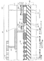
本発明に係る半導体装置の実施の形態1として、図1に半導体装置100の構成を示す。
【0059】
図1に示す半導体装置100は、図68を用いて説明した半導体装置90を例に採れば、RF回路部91の一部分を示しており、RF回路部RPとして示す。
【0060】
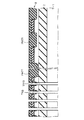
図1において、シリコン基板1と、該シリコン基板1上に配設された埋め込み酸化膜2と、埋め込み酸化膜2上に配設されたSOI層3とで構成されるSOI基板SB上に、RF回路部RPが配設されている。
【0061】
RF回路部RPにおいては、SOI層3のスパイラルインダクタSI(平面構成は図70参照)の配設領域に対応する領域が複数のトレンチ分離酸化膜11によって分割され、複数のSOI領域21が形成されている。トレンチ分離酸化膜11は、SOI層3の表面から埋め込み酸化膜2の表面に達するように配設されたトレンチ内にシリコン酸化膜を埋め込むことで形成され、各SOI領域21は電気的に完全に分離されている。
【0062】
なお、トレンチ分離酸化膜11は、所定の形成幅で、埋め込み酸化膜2の表面に対してほぼ垂直に延在する形状を有している。
【0063】
また、各SOI領域21の上部にはシリサイド膜31が配設され、それぞれ複数のトレンチ分離酸化膜11、SOI領域21、シリサイド膜31によって、PGシールド101(シールド層)が構成される。
【0064】
なお、トレンチ分離酸化膜11のように、電気的に完全に分離されたSOI領域を規定する分離酸化膜を完全分離酸化膜と呼称する。
【0065】
また、PGシールド101の形成領域はトレンチ分離酸化膜12によって規定され、PGシールド101の形成領域外においては、トレンチ分離酸化膜12によってSOI層3が分割され、SOI領域51および52が形成されている。トレンチ分離酸化膜12は完全分離酸化膜であり、SOI領域51および52は電気的に完全に分離されている。
【0066】
SOI領域51および52にはMOSトランジスタQ11およびQ12がそれぞれ形成されている。MOSトランジスタQ11およびQ12は、共にSOI領域51および52上に配設されたゲート絶縁膜GZ、ゲート絶縁膜GZ上に配設されたゲート電極GT、ゲート電極GT上に配設されたシリサイド膜GSおよび、それらの側面を覆うように配設されたサイドウォール絶縁膜GWを備えている。なお、MOSトランジスタQ11およびQ12は一般的なMOSトランジスタであり、その構成および製造方法に特徴があるものではない。
【0067】
また、MOSトランジスタQ11においては、サイドウォール絶縁膜GWの外側のSOI領域51の表面内に配設されたシリサイド膜SSおよびソース・ドレイン領域SDを示しているが、MOSトランジスタQ12においても同様の構成を有していることは言うまでもない。MOSトランジスタQ12は、ゲート電極GTの長手方向に沿った断面構成を表すので上述の構成が図示されていないだけである。
【0068】
そして、SOI基板SB上全域を覆うように、例えばシリコン酸化膜で構成される層間絶縁膜4が配設され、層間絶縁膜4上にはスパイラルインダクタSIをMOSトランジスタQ11に電気的に接続する配線WLが配設されている。配線WLの一方の端部は、層間絶縁膜4を貫通してMOSトランジスタQ11のシリサイド膜SSに達するコンタクト部CP1に接続されている。なお、コンタクト部CP1は、層間絶縁膜4を貫通するコンタクトホール内に導体を埋め込んで構成されている。
【0069】
また、層間絶縁膜4上を覆うように、例えばシリコン酸化膜で構成される層間絶縁膜5が配設され、層間絶縁膜5上にスパイラルインダクタSIが配設されている。スパイラルインダクタSIの一方の端部は層間絶縁膜5を貫通して配線WLに達するコンタクト部CPを介して配線WLに接続されている。
【0070】
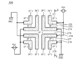
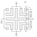
ここで、PGシールド101の平面視形状を図2に示す。図2に示すように、PGシールド101を構成する各SOI領域21は、それぞれ平面視形状が略L字型をなし、それぞれが対称に配設されている。
【0071】
すなわち、複数のSOI領域21は、相似形状の大小2種類のSOI領域21Lおよび21Sに分類され、SOI領域21SはSOI領域21Lの直交する2つのアームで規定される領域(内側領域と呼称)にSOI領域21Lと同様の配置形態となるように配設されている。
【0072】
そして、SOI領域21Lおよび21Sの1組を第1ユニットとすると、第1ユニットに対して線対称な形状に第2ユニットが配設され、さらに第1および第2ユニットに対して線対称な形状に第3および第4ユニットが配設された構成となっている。従って、PGシールド101は、4つのSOI領域21Sおよび4つのSOI領域21Lを有することになる。
【0073】
そして、4つのSOI領域21Lはそれぞれの2つアームの一方が、他のSOI領域21Lの2つのアームの一方と対向するように配設されているので、4つのSOI領域21Lで規定されるトレンチ分離酸化膜11の平面視形状は十字型をなしている。
【0074】
なお、図1に示すPGシールド101の構成は、例えば、図2におけるX−X線での断面に対応し、各SOI領域21は図1における層間絶縁膜4を貫通するしてシリサイド膜31に達するコンタクト部(図示せず)を介して所定の配線(図示せず)に電気的に接続され、当該配線を介して接地されることになる。
【0075】
<A−2.作用効果>
以上説明したように、PGシールド101はトレンチ分離酸化膜11によって電気的に分離された複数のSOI領域21およびシリサイド膜31の積層体で構成され、当該積層体はシリサイド膜31の存在により比較的低抵抗となるので、静電誘導損失を低減できるとともに、渦電流の経路がトレンチ分離酸化膜11により遮断されるので、渦電流に起因する電磁誘導損失を被ることがない。
【0076】
なお、静電誘導損失および電磁誘導損失の増加はインダクタの性能を表すQ値(インダクタに蓄えられるエネルギーを、各種損失で割った値)を減少させるので、静電誘導損失および電磁誘導損失を低減させることはQ値の向上に寄与することになる。
【0077】
また、トレンチ分離酸化膜11は、MOSトランジスタQ11およびQ12等が形成される素子形成領域のトレンチ分離酸化膜12の形成工程において、例えば共通のレジストマスクを用いてSOI層3を同時にパターニングすることで形成することができ、また、シリサイド膜31はMOSトランジスタQ11およびQ12のシリサイド膜GSおよびSSと同時に形成できるので、PGシールド101の形成のために新たな工程が増えることがなく、製造方法が複雑になることがない。
【0078】
また、PGシールド101はSOI層3内に形成されるので、PGシールドの形成のために新たな導体層は不要であり、装置構造が複雑になることもない。
【0079】
なお、以上の説明においてはトレンチ分離を用いて素子間分離を行う構成を示したが、LOCOS(Local Oxide of Silicon)分離やメサ分離などの他の素子間分離技術を用いても良いことは言うまでもない。これは、以下に説明する本発明に係る実施の形態2〜16のうち、トレンチ分離特有のディッシングの解決を目的とした実施の形態以外の実施の形態においても同様である。
【0080】
<A−3.変形例>
PGシールドの平面視形状は図2に示す形状に限定されるものではなく、渦電流の経路を遮断するような切り欠き部を備えるものであれば良い。
【0081】
図3〜図7にPGシールドの平面視形状の他の例を示す。
【0082】
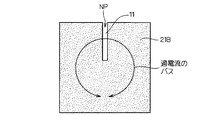
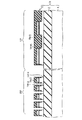
図3に示すPGシールドは、平面視形状が3角形の2つSOI領域21Aが、それぞれの底辺が対向するように配設されて第1ユニットを構成し、第1ユニットに対して線対称な形状に第2ユニットが配設され、さらに第1および第2ユニットに対して線対称な形状に第3および第4ユニットが配設された構成となっており、8つのSOI領域21Aを有している。なお、各SOI領域21Aの間にはトレンチ分離酸化膜11が配設されている。
【0083】
図4に示すPGシールドは、PGシールド全体の大きさに等しく、平面視形状が矩形のSOI領域21Bが、その中心部分にまで達する切り欠き部NPを有した構成となっている。切り欠き部NPにはトレンチ分離酸化膜11が配設されており、渦電流は切り欠き部NPにおいて遮断されることになる。
【0084】
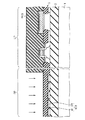
図5に示すPGシールドは、矩形の4つのSOI領域21Cが2行2列のマトリクス状に配設されて構成されている。なお、各SOI領域21Cの間にはトレンチ分離酸化膜11が配設されている。
【0085】
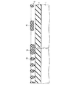
図6に示すPGシールドは、細長形状の4つのSOI領域21Dが、その長手方向の辺が互いに平行になるように一列に配設されている。なお、各SOI領域21Dの間にはトレンチ分離酸化膜11が配設されている。
【0086】
図7に示すPGシールドは、相似形状の大小3種類のL字型のSOI領域21L、21Mおよび21Sと、矩形のSOI領域21Eを有している。そして、SOI領域21MはSOI領域21Lの直交する2つのアームで規定される内側領域にSOI領域21Lと同様の配置形態となるように配設され、SOI領域21SはSOI領域21Mの直交する2つのアームで規定される内側領域にSOI領域21Mと同様の配置形態となるように配設され、SOI領域21EはSOI領域21Sの直交する2つのアームで規定される内側領域に配設されている。なお、各SOI領域21L、21M、21Sおよび21E間にはトレンチ分離酸化膜11が配設されている。
【0087】
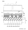
<B.実施の形態2>
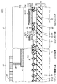
<B−1.装置構成>
本発明に係る半導体装置の実施の形態2として、図8に半導体装置200の構成を示す。
【0088】
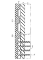
図8に示す半導体装置200は、図68を用いて説明した半導体装置90を例に採れば、RF回路部91およびロジック部92の一部分を示しており、それぞれRF回路部RPおよびロジック部LPとして示す。
【0089】
図8において、シリコン基板1と、該シリコン基板1上に配設された埋め込み酸化膜2と、埋め込み酸化膜2上に配設されたSOI層3とで構成されるSOI基板SB上に、RF回路部RPおよびロジック部LPが配設されている。
【0090】
RF回路部RPにおいては、SOI層3のスパイラルインダクタSI(平面構成は図70参照)の配設領域に対応する領域が複数のトレンチ分離酸化膜13によって分割され、複数のSOI領域22が形成されている。トレンチ分離酸化膜12は、SOI層3の表面から埋め込み酸化膜2の表面に達するように配設されたトレンチ内にシリコン酸化膜を埋め込むことで形成され、各SOI領域22は電気的に完全に分離されている。
【0091】
また、各SOI領域22の上部にはシリサイド膜32が配設され、それぞれ複数のトレンチ分離酸化膜13、SOI領域22、シリサイド膜32によって、PGシールド102(シールド層)が構成される。
【0092】
なお、トレンチ分離酸化膜13は、第1の形成幅で埋め込み酸化膜2の表面に対してほぼ垂直に延在する第1の部分と、第1の部分の下部に連続し、第1の形成幅よりも狭い第2の形成幅で埋め込み酸化膜2の表面に対してほぼ垂直に延在する第2の部分とで構成されている。
【0093】
なお、PGシールド102の平面視形状は、例えば図2を用いて説明した形状を採用しても良いし、図3〜図7を用いて説明した形状を採用しても良い。
【0094】
また、RF回路部RPとロジック部LPとの間はトレンチ分離酸化膜14によって電気的に分離され、ロジック部LPにおいては、トレンチ分離酸化膜15によってSOI層3が分割され、SOI領域61および62が形成されている。
【0095】
なお、トレンチ分離酸化膜15のように、SOI領域を電気的に完全に分離するのではなく、その下部にSOI層3がウエル領域WRとして配設された分離酸化膜を部分分離酸化膜と呼称する。
【0096】
<B−1−1.部分分離酸化膜について>
ここで、部分分離酸化膜について簡単に説明する。完全分離酸化膜によって他の素子から電気的に完全に分離されたMOSトランジスタにおいては、他のMOSトランジスタとの間でのラッチアップが原理的に起こらない。
【0097】
従って、完全分離酸化膜を用いてCMOSトランジスタを有するSOIデバイスを製造する場合は、微細加工技術で決まる最小分離幅を使用できチップ面積を縮小できるメリットがあった。しかしながら、衝突電離現象によって発生するキャリア(NMOSではホール)がチャネル形成領域(ボディ領域)に溜まり、これによりキンクが発生したり、動作耐圧が劣化したり、また、チャネル形成領域の電位が安定しないために遅延時間の周波数依存性が発生する等の基板浮遊効果による影響があった。
【0098】
このようなチャネル形成領域の電位の変動に関しては、「IEEE TRANSACTIONS ON ELECTRON DEVICES, VOL.45, NO.7, JULY 1998, pp1479-1484, "Analysis of Delay Time Instability According to the Operating Frequency in Field Shield Isolated SOI Circuits" S.Maeda et al.」(文献1)に具体的に記載されている。つまり、ボディ領域の電位が過渡的に変動するため、これに伴って、トランジスタの特性も過渡的に変動し、回路動作が不安定になるということである(文献1の図7参照)。
【0099】
また、文献1の図5で示されるようにディレイタイムに周波数依存性が表れることも検証されている。
【0100】
そこで考案されたのが、パーシャルトレンチ分離とも呼称される部分分離酸化膜であり、図8の構成を例に採れば、トレンチ分離酸化膜15の下部のウエル領域WRを通じてキャリアの移動が可能であり、キャリアがチャネル形成領域に溜まるということを防止でき、またウエル領域WRを通じてチャネル形成領域の電位を固定することができるので、基板浮遊効果による種々の問題が発生しない。
【0101】
図8においては部分分離酸化膜と完全分離酸化膜とを併用した構成を示しているが、部分分離酸化膜と完全分離酸化膜との併用例およびその製造方法については、特許出願番号11−177091の明細書中の図4〜図7および図8〜図27に開示されている。
【0102】
また、部分分離酸化膜と完全分離酸化膜とを併用する場合に、分離酸化膜の一方側が完全分離酸化膜の形状となり、他方側が部分分離酸化膜の形状となった併合分離酸化膜を使用することがあるが、併合分離酸化膜の構成およびその製造方法については、特許出願番号2000−39480の明細書中の図1〜図38に開示されている。
【0103】
また、部分分離酸化膜の断面形状については、「"IEEE International SOI Conference,Oct.1999,pp131-132,"Bulk-Layout-Compatible 0.18μm SOI-CMOS Technology Using Body-Fixed Partial Trench Isolation(PIT)" Y.Hirano et al.」(文献2)の図2としてSEM写真を用いて示されている。
【0104】
ここで、図8の説明に戻る。図8のロジック部LPにおいて、SOI領域61および62にはMOSトランジスタQ21およびQ22がそれぞれ形成されている。
【0105】
MOSトランジスタQ21およびQ22は、図1に示したMOSトランジスタQ11およびQ12と同様に一般的なMOSトランジスタであり、基本的な構成要素は同じであるので、MOSトランジスタQ11およびQ12と同じ構成については同じ符号を付し、重複する説明は省略する。
【0106】
その他、図1に示した半導体装置100と同一の構成については同一の符号を付し、重複する説明は省略する。
【0107】
<B−2.製造方法>
次に、製造工程を順に示す図9〜図11を用いて半導体装置200の製造方法について説明する。
【0108】
まず、SOI基板SBを準備し、図9に示す工程において、SOI層3上に厚さ20nm程度のシリコン酸化膜OXおよび厚さ200nm程度のシリコン窒化膜SNを順次形成した後、パターニングしたレジストマスクRM1を用いて、シリコン酸化膜OX、シリコン窒化膜SNおよびSOI層3の多層膜を、SOI層3の下層部が残るようにエッチングし、トレンチ分離酸化膜13、14および15が形成される領域にトレンチTR131、TR141およびTR15を形成する。
【0109】
次に、図10に示す工程において、トレンチTR131、TR141の一部を覆うとともに、トレンチTR15を完全に覆うレジストマスクRM2を用いて、トレンチTR131、TR141のレジストマスクRM2で覆われない部分をさらにエッチングすることによりSOI層3を貫通するトレンチTR13およびTR14を形成する。
【0110】
次に、レジストマスクRM2を除去した後、全面に渡って厚さ500nm程度のシリコン酸化膜を形成して、トレンチTR13〜TR15を埋め込み、CMP(Chemical Mechanical Polishing)処理によりシリコン窒化膜SNの途中まで研磨し、その後、シリコン窒化膜SNおよびシリコン酸化膜OXを除去することで、図11に示すようにトレンチ分離酸化膜13〜15を得る。
【0111】
なお、この後は、既存のMOSトランジスタの製造工程(既存のサリサイド工程を含む)、層間絶縁膜の製造工程、配線層の製造工程、スパイラルインダクタの製造工程等を経て、半導体装置200を得る。
【0112】
<B−3.作用効果>
以上説明したように、PGシールド102はトレンチ分離酸化膜13によって電気的に分離された複数のSOI領域22およびシリサイド膜32の積層体で構成され、当該積層体はシリサイド膜32の存在により比較的低抵抗となるので、静電誘導損失を低減できるとともに、渦電流の経路がトレンチ分離酸化膜13により遮断されるので、渦電流による電磁誘導損失を被ることがない。
【0113】
また、トレンチ分離酸化膜13は、ロジック部LPとRF回路部RPとの境界のトレンチ分離酸化膜14およびロジック部LPのMOSトランジスタQ21とQ22との分離に使用されるトレンチ分離酸化膜15の形成工程において、共通のレジストマスクRM1およびRM2を用いて形成することができ、また、シリサイド膜32はMOSトランジスタQ21およびQ22のシリサイド膜GSおよびSSと同時に形成できるので、PGシールド102の形成のために新たな工程が増えることがなく、製造方法が複雑になることがない。
【0114】
なお、トレンチ分離酸化膜13の上部端縁部の形状を、トレンチ分離酸化膜14および15の上部端縁部の形状と同じにできるという特徴もある。
【0115】
また、PGシールド102はSOI層3内に形成されるので、PGシールドの形成のために新たな導体層は不要であり、装置構造が複雑になることもない。
【0116】
また、ロジック部LPにおいては部分分離酸化膜であるトレンチ分離酸化膜15により素子間を分離するので、トレンチ分離酸化膜15の下部のウエル領域WRを通じてチャネル形成領域(ボディ領域)の電位を固定することができ、基板浮遊効果による種々の問題を防止できる。
【0117】
<B−4.変形例>
PGシールド102においては、トレンチ分離酸化膜13は、トレンチ分離酸化膜14およびトレンチ分離酸化膜15の形成工程において、共通のレジストマスクRM1およびRM2を用いて形成される例を示したが、工程がやや複雑になることを許容できるのであれば、図1を用いて説明した半導体装置100のトレンチ分離酸化膜11のように、単純な断面形状としても良い。
【0118】
<C.実施の形態3>
<C−1.装置構成>
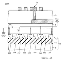
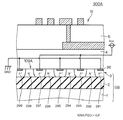
本発明に係る半導体装置の実施の形態3として、図12に半導体装置300の構成を示す。
【0119】
図12に示す半導体装置300は、図8に示す半導体装置200と同様に、SOI基板SB上に、RF回路部RPおよびロジック部LPが配設された構成を示している。
【0120】
RF回路部RPにおいては、スパイラルインダクタSI(平面構成は図70参照)の配設領域に対応する埋め込み酸化膜2上に、独立した複数のSOI領域23が形成され、PGシールド103(シールド層)を構成している。そして、PGシールド103は全体がトレンチ分離酸化膜16で覆われている。
【0121】
なお、PGシールド103の平面視形状は、例えば図2を用いて説明した形状を採用しても良いし、図3〜図7を用いて説明した形状を採用しても良い。
【0122】
また、ロジック部LPにおいては、部分分離酸化膜であるトレンチ分離酸化膜15によってSOI層3が分割され、SOI領域71および72が形成されている。そして、SOI領域71および72にはMOSトランジスタQ31およびQ32がそれぞれ形成されている。
【0123】
MOSトランジスタQ31およびQ32は、図1に示したMOSトランジスタQ11およびQ12と同様に一般的なMOSトランジスタであり、基本的な構成要素は同じであるので、MOSトランジスタQ11およびQ12と同じ構成については同じ符号を付し、重複する説明は省略する。
【0124】
その他、図1に示した半導体装置100と同一の構成については同一の符号を付し、重複する説明は省略する。
【0125】
SOI領域23は、半導体装置200の製造方法を示す図10を用いて説明すると、RF回路部RPにおいて、トレンチTR141のレジストマスクRM2で覆われない部分をさらにエッチングしてSOI層3を貫通するトレンチTR14を形成する。その後、レジストマスクRM2を除去して、シリコン酸化膜OX、シリコン窒化膜SNを完全に除去するとともに、SOI層3の一部を除去することで形成できる。なお、この場合、ロジック部LPにおいてはシリコン酸化膜OX、シリコン窒化膜SNが除去されないように、レジストマスクで覆うことになる。
【0126】
そして、SOI領域23の形成後は、ロジック部LPのレジストマスクを除去し、全面に渡ってシリコン酸化膜を形成して、トレンチTR15を埋め込むとともに、SOI領域23の形成に際して形成されたトレンチを埋め込み、CMP処理によりロジック部LPに残るシリコン窒化膜SNの途中まで研磨し、その後、シリコン窒化膜SNおよびシリコン酸化膜OXを除去することで、トレンチ分離酸化膜16および15を得る。
【0127】
なお、SOI領域23は、いわゆるボディ領域の基部に相当する領域であり、その厚さはトレンチ分離酸化膜15の下部のウエル領域WRの厚さに等しくなる。
【0128】
<C−2.作用効果>
以上説明したように、PGシールド103はトレンチ分離酸化膜16によって覆われた複数の独立したSOI領域23で構成されているので、静電誘導損失を低減できるとともに、渦電流の経路がトレンチ分離酸化膜16により遮断されるので、渦電流による電磁誘導損失を被ることがない。
【0129】
また、PGシールド103はSOI層3を分割して形成されるので、PGシールドの形成のために新たな導体層は不要であり、装置構造が複雑になることもない。
【0130】
また、ロジック部LPにおいては部分分離酸化膜であるトレンチ分離酸化膜15により素子間を分離するので、トレンチ分離酸化膜15の下部のウエル領域WRを通じてチャネル形成領域(ボディ領域)の電位を固定することができ、基板浮遊効果による種々の問題を防止できる。
【0131】
<C−3.変形例1>
以上説明したPGシールド103は、独立した複数のSOI領域23で構成されている。これは、SOI層3にはウエル注入(あるいはチャネル注入とも呼称される)が行われるため、シリコン基板1よりも低抵抗になっているので、SOI領域23を導体として使用するものであるが、さらに抵抗値を下げたい場合には、SOI領域23に不純物を比較的高濃度に注入すれば良い。図13にその工程の一例を示す。
【0132】
すなわち図13に示すように、少なくともトレンチ分離酸化膜16までが形成された状態(図13においてはMOSトランジスタQ31およびQ32が形成された状態を例示)のSOI基板SBにおいて、ロジック部LP上および不純物を注入しない部分上にレジストマスクRM3を形成し、トレンチ分離酸化膜16を介してイオン注入により不純物を注入する。そのドーズ量は1×10¹⁴〜1×10¹⁶/cm2である。
【0133】
なお不純物の注入は上記方法に限定されるものではなく、PGシールド103を形成した後、素子分離酸化膜16を形成する前に行っても良く、また、PGシールド103上に対応する素子分離酸化膜16を除去し、SOI領域23を露出させた状態で行っても良い。
【0134】
<C−4.変形例2>
また、図14に示す半導体装置300Aのように、それぞれのSOI領域23の上部にシリサイド膜33を形成したPGシールド103A(シールド層)を使用しても良い。
【0135】
PGシールド103Aは、図12に示すPGシールド103を形成後、素子分離酸化膜16で一旦覆った後、PGシールド103上に対応する素子分離酸化膜16を除去して開口部161を形成してSOI領域23を露出させる。その後、ロジック部LPのMOSトランジスタQ31およびQ32の形成に際してのサリサイド工程において、露出したSOI領域23上にシリサイド膜33を同時に形成する。なお、トレンチ分離酸化膜16の開口部161は、後に、層間絶縁膜によって埋め込まれることになる。
【0136】
このように、SOI領域23上にシリサイド膜33を備えたPGシールド103Aは、PGシールド103よりも低抵抗となるので、静電誘導損失防止の効果が高まる。
【0137】
<D.実施の形態4>
<D−1.装置構成>
本発明に係る半導体装置の実施の形態4として、図15に半導体装置400の構成を示す。
【0138】
図15に示す半導体装置400は、図12に示す半導体装置300と同様に、SOI基板SB上に、RF回路部RPおよびロジック部LPが配設された構成を示している。
【0139】
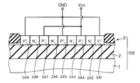
RF回路部RPにおいては、スパイラルインダクタSI(平面構成は図70参照)の配設領域に対応するSOI層3内に、互いに密接したSOI領域241〜249で構成されるPGシールド104(シールド層)が形成されている。
【0140】
また、RF回路部RPとロジック部LPとの間には部分分離酸化膜であるトレンチ分離酸化膜15が配設され、ロジック部LPにおいては、トレンチ分離酸化膜15によってSOI層3が分割され、SOI領域71および72が形成されている。そして、SOI領域71および72にはMOSトランジスタQ31およびQ32がそれぞれ形成されている。
【0141】
なお、その他、図12を用いて説明した半導体装置300と同一の構成については同一の符号を付し、重複する説明は省略する。
【0142】
PGシールド104を構成するSOI領域241〜249は、隣り合う領域どうしで、それぞれ不純物濃度あるいは不純物の導電型が異なるように構成され、PNジャンクションにより渦電流を遮断するように構成されている。
【0143】
図15においては、SOI領域241〜249が、それぞれP-(P型不純物を低濃度に含む)領域、P+(P型不純物を高濃度に含む)領域、P-領域、N+(N型不純物を高濃度に含む)領域、P-領域、P+領域、P-領域、N+領域、P-領域となっている。
【0144】
ここで、図16にPGシールド104の平面視形状を示す。PGシールド104の平面視形状は、図2を用いて説明したPGシールド101の形状と同様であり、形状についての説明は省略するが、PGシールド101においてはトレンチ分離酸化膜11であった部分がSOI領域となっている点と、シリサイド膜11が配設されていない点とが大きく異なっている。なお、図16におけるX−X線での断面が、図15に示すPGシールド104の構成に対応する。
【0145】
PGシールド104においては、PGシールド101のように全てのSOI領域が接地される構成ではなく、渦電流を遮断するために、PNジャンクションにより構成されるダイオードに逆バイアスを与えるので、電源電位(Vcc)に接続されるものがある。
【0146】
例えば、図16においては、SOI領域242および246が接地電位に接続され、SOI領域244および248が電源電位に接続され、SOI領域241、243、245、247および249は隣接するP+領域を介して接地される。なお、以上の説明においては、SOI領域244および248が電源電位に接続されるが、このように電源電位に接続される構成を含んでいても、便宜的にPGシールド(Perforated Ground Shield)と呼称する。これは、以下に説明する他の実施の形態においても同じである。
【0147】
<D−2.作用効果>
以上説明した接続により、SOI領域242、243、244、SOI領域244、245、246、SOI領域246、247、248で構成されるダイオードに逆バイアスが与えられ、渦電流を発生させる逆起電力により順バイアスされることが防止され、渦電流に起因する電磁誘導損失を被ることなく静電誘導損失を低減できる。
【0148】
また、PGシールド104は、接地されたP+領域(低抵抗領域)を通じて静電誘導による電流を流すので、静電誘導損失を低減できることは言うまでもなく、PGシールド104はSOI層3内に形成されるので、PGシールドの形成のために新たな導体層は不要であり、装置構造が複雑になることもない。
【0149】
また、ロジック部LPにおいては部分分離酸化膜であるトレンチ分離酸化膜15により素子間を分離するので、トレンチ分離酸化膜15の下部のウエル領域WRを通じてチャネル形成領域(ボディ領域)の電位を固定することができ、基板浮遊効果による種々の問題を防止できる。
【0150】
<D−3.変形例1>
以上の説明においては、PGシールド104の平面視形状は、図2を用いて説明したPGシールド101と同じものとして説明したが、図3〜図7を用いて説明した形状を採用しても良い。ただし、その場合には、SOI領域の不純物の注入状態が異なることになる。
【0151】
すなわち、図3に示す形状においては、図3に向かって、例えば、右側最上部のSOI領域21AをP+領域とすれば、時計回りに隣り合うSOI領域21Aとの間の領域(図3にはトレンチ分離酸化膜11となっている領域)はP-領域とし、以下、時計回りにN+領域、P-領域、P+領域、P-領域を順に形成し、N+領域は電源電位に接続し、P+領域は接地することでダイオードを逆バイアスすることができる。
【0152】
また、図5に示す形状においては、図5に向かって、例えば、右側最上部のSOI領域21CをP+領域とすれば、時計回りに隣り合うSOI領域21Cとの間はP-領域とし、以下、時計回りにN+領域、P-領域、P+領域、P-領域を順に形成し、N+領域は電源電位に接続し、P+領域は接地することでダイオードを逆バイアスすることができる。
【0153】
また、図6に示す形状においては、例えば、最上部のSOI領域21DをP+領域とすれば、その下のSOI領域21Dとの間はP-領域とし、以下、N+領域、P-領域、P+領域、P-領域を順に形成し、N+領域は電源電位に接続し、P+領域は接地することでダイオードを逆バイアスすることができる。
【0154】
また、図7に示す形状においては、例えば、SOI領域21EをP+領域とすればSOI領域21Sとの間はP-領域とし、SOI領域21SはN+領域、SOI領域21Sと21Mとの間はP-領域、SOI領域21MはP+領域、SOI領域21Mと21Lとの間はP-領域、SOI領域21LはN+領域とし、N+領域は電源電位に接続し、P+領域は接地することでダイオードを逆バイアスすることができる。
【0155】
<D−4.変形例2>
図15に示したPGシールド104においては、低濃度不純物領域(P-領域)の左右のSOI領域はP+領域およびN+領域となっていたが、低濃度不純物領域の左右を同じ導電型にしても良い。
【0156】
すなわち、PGシールド104部分を示す図17に示すように、SOI領域242、244、246および248をN-領域とし、他の領域を全てP+領域としても良い。
【0157】
そして、SOI領域243および247を電源電位に接続し、SOI領域241、245および249を接地することで、SOI領域241および242で構成されるダイオード、SOI領域248および249で構成されるダイオード、SOI領域245および246で構成されるダイオード、SOI領域244および245で構成されるダイオードに逆バイアスが与えられ、渦電流を発生させる逆起電力により順バイアスされることが防止され、渦電流に起因する電磁誘導損失を被ることなく静電誘導損失を低減できる。
【0158】
また、SOI領域が2種類だけで済むので、その注入工程においては注入マスクの重ね合わせ回数が少なくなり、マスクの重ね合わせに必要なマージンを小さくできるので、SOI領域のパターンを微細化できる。
【0159】
なお、以上の説明では、SOI領域をN-領域とP+領域の2種類としたが、P-領域とN+領域の2種類としても良いことは言うまでもない。
【0160】
<E.実施の形態5>
<E−1.装置構成>
本発明に係る半導体装置の実施の形態5として、図18に半導体装置500の構成を示す。
【0161】
図18に示す半導体装置500は、図12に示す半導体装置300と同様に、SOI基板SB上に、RF回路部RPおよびロジック部LPが配設された構成を示している。
【0162】
RF回路部RPにおいては、スパイラルインダクタSI(平面構成は図70参照)の配設領域に対応するSOI層3内に、互いに密接したSOI領域261〜269で構成されるPGシールド105(シールド層)が形成されている。そして、PGシールド105上は部分分離酸化膜であるトレンチ分離酸化膜17で覆われている。
【0163】
トレンチ分離酸化膜17はロジック部LPまで延在し、ロジック部LPにおいては、トレンチ分離酸化膜15によってSOI層3が分割され、SOI領域71および72が形成されている。そして、SOI領域71および72にはMOSトランジスタQ31およびQ32がそれぞれ形成されている。
【0164】
なお、その他、図12を用いて説明した半導体装置300と同一の構成については同一の符号を付し、重複する説明は省略する。
【0165】
PGシールド105を構成するSOI領域261〜269は、隣り合う領域どうしで、それぞれ不純物濃度あるいは不純物の導電型が異なるように構成され、PNジャンクションにより渦電流を遮断するように構成されている。
【0166】
図18においては、SOI領域261〜269が、それぞれP-領域、P+領域、P-領域、N+領域、P-領域、P+領域、P-領域、N+領域、P-領域となっており、その平面視形状、電源電位および接地電位への接続、および動作は図15を用いて説明したPGシールド104と同じである。
【0167】
なお、電源電位および接地電位への接続は、例えば図18に示すように、層間絶縁膜4およびトレンチ分離酸化膜17を貫通してSOI領域268(N+領域)に達するようにコンタクト部CP2を設け、コンタクト部CP2に電源電位あるいは接地電位に繋がる配線WL1を接続するようにすれば良い。
【0168】
<E−2.作用効果>
以上説明した半導体装置500においては、図15を用いて説明した半導体装置400と同様に、PGシールド105において渦電流を遮断することができ、渦電流による電磁誘導損失を被ることがない。
【0169】
また、PGシールド105は、接地されたP+領域(低抵抗領域)を通じて静電誘導による電流を流すので、静電誘導損失を低減できることは言うまでもなく、PGシールド105はSOI層3内に形成されるので、PGシールドの形成のために新たな導体層は不要であり、装置構造が複雑になることもない。
【0170】
また、トレンチ分離酸化膜17は、ロジック部LPにおいてトレンチ分離酸化膜15を形成する工程で同時に形成でき、またSOI領域への不純物の注入も容易なので製造工程が複雑になることを防止できる。
【0171】
すなわち、トレンチ分離酸化膜15および17を、図9〜図11を用いて説明したのと同様の工程で形成した後、図13を用いて説明した工程のように、トレンチ分離酸化膜17の上部から、トレンチ分離酸化膜17下部のSOI層にP型不純物およびN型不純物を選択的にイオン注入することでPGシールド105を形成できる。
【0172】
また、ロジック部LPにおいては部分分離酸化膜であるトレンチ分離酸化膜15により素子間を分離するので、トレンチ分離酸化膜15の下部のウエル領域WRを通じてチャネル形成領域(ボディ領域)の電位を固定することができ、基板浮遊効果による種々の問題を防止できる。
【0173】
<F.実施の形態6>
実施の形態5において説明した半導体装置500においては、PGシールド105上が部分分離酸化膜であるトレンチ分離酸化膜17で覆われた構成を示したが、PGシールドはスパイラルインダクタSIの平面方向の配設面積と少なくとも同等の面積を有するように形成されるので、広い面積に渡ってトレンチ分離酸化膜17を設ける必要がある。
【0174】
ここで、トレンチ分離酸化膜の形成においては、トレンチに酸化膜を埋め込んだ後、不要な酸化膜をCMP処理で除去するが、トレンチ分離酸化膜を広い面積に渡って形成する場合には、当該トレンチ分離酸化膜が皿状に窪むディッシングが発生しやすくなる。
【0175】
図19にディッシングが発生した状態を示す。図19において、広い面積のトレンチ分離酸化膜17Aの表面が皿状に窪んでおり、狭い面積のトレンチ分離酸化膜15は正常に形成されている。
【0176】
ディッシングが発生したトレンチ分離酸化膜の上部端縁部の形状は、正常なトレンチ分離酸化膜の上部端縁部の形状とは異なり、MOSトランジスタの特性に影響を及ぼす可能性がある。
【0177】
本発明に係る半導体装置の実施の形態6においては、このようなディッシングの発生を防止した構成について説明する。
【0178】
<F−1.装置構成>
本発明に係る半導体装置の実施の形態6として、図20に半導体装置600の構成を示す。
【0179】
図20に示す半導体装置600は、図12に示す半導体装置300と同様に、SOI基板SB上に、RF回路部RPおよびロジック部LPが配設された構成を示している。
【0180】
RF回路部RPにおいては、スパイラルインダクタSI(平面構成は図70参照)の配設領域に対応するSOI層3内に、互いに密接したSOI領域271〜279および、SOI領域272、274、276および278上に形成されたシリサイド膜34で構成されるPGシールド106(シールド層)が形成されている。
【0181】
ここで、SOI領域271、273、275、277および279は、他のSOI領域よりも厚さが薄く、その上部には部分分離酸化膜であるトレンチ分離酸化膜18が形成されている。なお、SOI領域271上のトレンチ分離酸化膜はロジック部LPまで延在している。
【0182】
そして、ロジック部LPにおいては、トレンチ分離酸化膜15によってSOI層3が分割され、SOI領域71および72が形成されている。そして、SOI領域71および72にはMOSトランジスタQ31およびQ32がそれぞれ形成されている。
【0183】
なお、その他、図12を用いて説明した半導体装置300と同一の構成については同一の符号を付し、重複する説明は省略する。
【0184】
PGシールド106を構成するSOI領域271〜279は、隣り合う領域どうしで、それぞれ不純物濃度あるいは不純物の導電型が異なるように構成され、PNジャンクションにより渦電流を遮断するように構成されている。
【0185】
図20においては、SOI領域271〜279が、それぞれP-領域、N+領域、P-領域、P+領域、P-領域、N+領域、P-領域、P+領域、P-領域となっており、P-領域上にトレンチ分離酸化膜18が形成されている。
【0186】
ここで、図21にPGシールド106の平面視形状を示す。PGシールド106の平面視形状は、図2を用いて説明したPGシールド101の形状と同様であり、形状についての説明は省略する。なお、図21におけるX−X線での断面が、図20に示すPGシールド106の構成に対応する。
【0187】
図21においては、渦電流を遮断するために、PNジャンクションにより構成されるダイオードに逆バイアスを与えるので、SOI領域272および276が電源電位(Vcc)に接続され、SOI領域274および278が接地されている。
【0188】
<F−2.作用効果>
以上説明した半導体装置600においては、PGシールド106の形成領域には面積の狭いトレンチ分離酸化膜18を形成するので、ディッシングの発生を防止できる。
【0189】
また、図15を用いて説明した半導体装置400と同様に、PGシールド106において渦電流による電磁誘導損失を低減できる。
【0190】
また、PGシールド106は、接地されたP+領域(高抵抗領域)を通じて静電誘導による電流を流すので、静電誘導損失を低減できることは言うまでもなく、PGシールド106はSOI層3内に形成されるので、PGシールドの形成のために新たな導体層は不要であり、装置構造が複雑になることもない。
【0191】
また、トレンチ分離酸化膜18は、ロジック部LPにおいてトレンチ分離酸化膜15を形成する工程で同時に形成でき、シリサイド膜34の形成もSOI領域への不純物の注入も容易なので、製造工程が複雑になることを防止できる。
【0192】
すなわち、トレンチ分離酸化膜15および18を、図9〜図11を用いて説明したのと同様の工程で形成した後、ロジック部LPのMOSトランジスタQ31およびQ32の形成に際してのサリサイド工程において、露出したSOI領域上にシリサイド膜34を同時に形成し、PGシールド106の形成領域において、P型不純物およびN型不純物を選択的にイオン注入することでPGシールド106を形成できる。
【0193】
また、ロジック部LPにおいては部分分離酸化膜であるトレンチ分離酸化膜15により素子間を分離するので、トレンチ分離酸化膜15の下部のウエル領域WRを通じてチャネル形成領域(ボディ領域)の電位を固定することができ、基板浮遊効果による種々の問題を防止できる。
【0194】
<F−3.変形例>
図20に示した半導体装置600のPGシールド106においては、低濃度不純物領域(P-領域)の左右のSOI領域はP+領域およびN+領域となっていたが、低濃度不純物領域の左右を同じ導電型にしても良い。
【0195】
半導体装置600の変形例として、図22に半導体装置600Aを示す。図22におけるPGシールド106A(シールド層)は、SOI領域271、273、275、277および249をN-領域とし、他の領域を全てP+領域としている。
【0196】
ここで、図23にPGシールド106Aの平面視形状を示す。PGシールド106Aの平面視形状は、図2を用いて説明したPGシールド101の形状と同様であり、形状についての説明は省略する。なお、図23におけるX−X線での断面が、図22に示すPGシールド106Aの構成に対応する。
【0197】
図23においては、渦電流を遮断するために、PNジャンクションにより構成されるダイオードに逆バイアスを与えるので、SOI領域272および276が電源(Vcc)に接続され、SOI領域274および278が接地されている。
【0198】
このように接続することで、SOI領域273および274で構成されるダイオード、SOI領域274および275で構成されるダイオード、SOI領域277および278で構成されるダイオードに逆バイアスが与えられ、渦電流を発生させる逆起電力により順バイアスされることが防止され、渦電流に起因する電磁誘導損失を被ることなく静電誘導損失を低減できる。
【0199】
また、SOI領域が2種類だけで済むので、その注入工程においては注入マスクの重ね合わせ回数が少なくなり、マスクの重ね合わせに必要なマージンを小さくできるので、SOI領域のパターンを微細化できる。
【0200】
なお、以上の説明では、SOI領域をN-領域とP+領域の2種類としたが、P-領域とN+領域の2種類としても良いことは言うまでもない。
【0201】
<G.実施の形態7>
以上説明した実施の形態6においては、PGシールド形成領域におけるトレンチ分離酸化膜のディッシングを防止するための構成について示したが、以下に説明する実施の形態7の構成のようにしても良い。
【0202】
<G−1.装置構成>
本発明に係る半導体装置の実施の形態7として、図24に半導体装置700の構成を示す。なお、図24においては簡単化のためRF回路部RPの構成だけを示している。
【0203】
図24に示すようにRF回路部RPにおいては、スパイラルインダクタSI(平面構成は図70参照)の配設領域に対応するSOI層3内に、互いに密接したSOI領域281〜287、およびSOI領域282、284および286上に形成されたシリサイド膜35で構成されるPGシールド107(シールド層)が形成されている。
【0204】
ここで、SOI領域281、283、285および287は、他のSOI領域よりも厚さが薄く、その上部には部分分離酸化膜であるトレンチ分離酸化膜19が形成されている。なお、SOI領域281および287上のトレンチ分離酸化膜19は他のトレンチ分離酸化膜17よりも広く形成されている。
【0205】
そして、SOI領域282、284および286上のシリサイド膜35には、層間絶縁膜4を貫通して配設されたコンタクト部CP3が接続され、当該コンタクト部は層間絶縁膜4上に配設された接地に繋がる配線WL2に接続されている。
【0206】
なお、その他、図12を用いて説明した半導体装置300と同一の構成については同一の符号を付し、重複する説明は省略する。
【0207】
PGシールド107を構成するSOI領域281〜287は、SOI領域282、284および286が全てP+領域となり、SOI領域281、283、285および287がN-領域となっており、PNジャンクションにより渦電流を遮断するように構成されている。
【0208】
ここで、図25にPGシールド107の平面視形状を示す。PGシールド107の平面視形状は、シリサイド膜を有する矩形のSOI領域28(SOI領域282、284および286の総称)が、互いに間隔を開けてマトリクス状に配設された形状をなし、各SOI領域28の間にトレンチ分離酸化膜19が配設されている。
【0209】
なお、図25におけるY−Y線での断面が、図24に示すPGシールド107の構成に対応し、配線WL2は飛び飛びに配設されたSOI領域282、284および286上を辿るようにL字型に配設されている。
【0210】
また、シリサイド膜を有する他のSOI領域28上にも配線が配設されるが、その配線経路は4隅のSOI領域28以外は上記L字型となるように配設されており、各配線に与えられる電位は接地電位と電源電位が交互に与えられる。
【0211】
また、PGシールド107から離れた位置には低濃度不純物領域を電源電位に接続するためのコンタクト領域CRが配設されている。
【0212】
<G−2.作用効果>
このように接続することで、低濃度のSOI領域と高濃度のSOI領域で構成される全てのダイオードに逆バイアスが与えられ、渦電流を発生させる逆起電力により順バイアスされることが防止され、渦電流に起因する電磁誘導損失を被ることなく静電誘導損失を低減できる。
【0213】
また、PGシールド107は、接地されたP+領域(高抵抗領域)を通じて静電誘導による電流を流すので、静電誘導損失を低減できることは言うまでもなく、PGシールド107はSOI層3内に形成されるので、配線WL2の形成のための工程が必要となるものの、PGシールドの形成のために新たな導体層は不要であり、装置構造が複雑になることもない。
【0214】
<G−3.変形例1>
以上説明した半導体装置700においては、PGシールド107のSOI領域を配線WL2で電気的に接続する構成について説明したが、配線WL2の代わりに図26に示す半導体装置700Aのようにゲート配線を使用しても良い。
【0215】
すなわち、図26に示す半導体装置700AのPGシールド107A(シールド層)においては、SOI領域282、284および286上にはシリサイド膜は有さず、MOSトランジスタのゲート電極と同じ工程で形成された連続するゲート配線GTLがSOI領域282、284および286に直接に接する構成となっている。
【0216】
なお、トレンチ分離酸化膜19上には、MOSトランジスタのゲート絶縁膜と同じ工程で形成された絶縁膜GZLが配設され、ゲート配線GTL上にはMOSトランジスタのシリサイド膜と同じ工程で形成されたシリサイド膜GSLが配設されている。
【0217】
なお、ゲート配線GTLの平面視形状は、図25を用いて説明した配線WL2と同様に、L字型に配設されている。
【0218】
このような構成とすることで、SOI領域を電気的に接続するための配線の製造工程を簡略化できる。
【0219】
<G−4.変形例2>
また、半導体装置700においては、部分分離酸化膜であるトレンチ分離酸化膜19で覆われたSOI領域と、それ以外のSOI領域との間でのPNジャンクションにより渦電流を遮断する構成を示したが、トレンチ分離酸化膜19の代わりに、図27および図28で示す半導体装置700Bおよび700Cのように、完全分離酸化膜を用いて電気的に完全に分離されたSOI領域を形成するようにしても良い。
【0220】
図27に示す半導体装置700BのPGシールド107B(シールド層)は、完全分離酸化膜であるトレンチ分離酸化膜191によって電気的に完全に分離されている。
【0221】
図28に示す半導体装置700CのPGシールド107C(シールド層)は、完全分離酸化膜であるトレンチ分離酸化膜192によって電気的に完全に分離されている。
【0222】
PGシールド107Bも107Cも、SOI領域を完全に分離する点では同じであるが、トレンチ分離酸化膜192は、図示しないロジック部において、MOSトランジスタ間を部分分離する場合に、共通のレジストマスクを用いて形成することができ、新たな工程が増えることがなく、製造方法を簡略化することができる。
【0223】
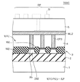
<H.実施の形態8>
<H−1.装置構成>
本発明に係る半導体装置の実施の形態8として、図29に半導体装置800の構成を示す。なお、図29に示す半導体装置800は、簡単化のためRF回路部RPの構成だけを示している。
【0224】
図29に示すようにRF回路部RPにおいては、スパイラルインダクタSI(平面構成は図70参照)の配設領域に対応するSOI層3内に、互いに密接したSOI領域291〜299と、SOI領域291、293、295、297および299上に形成されたシリサイド膜36とで構成されるPGシールド108(シールド層)が形成されている。
【0225】
そして、SOI領域292、294、296および298の上部にはMOSトランジスタのゲート電極と同じ断面構造を有する擬似ゲート電極MD1が配設されている。擬似ゲート電極MD1は、図示しないMOSトランジスタと同様に、ゲート絶縁膜DGZ、ゲート電極DGT、シリサイド膜DGSおよびサイドウォール絶縁膜DGWを有している。
【0226】
なお、シリサイド膜36は擬似ゲート電極MD1のサイドウォール絶縁膜DGWの外側のSOI領域291、293、295、297および299上に配設されている。
【0227】
そして、SOI領域291、293、295、297および299はN+領域となっており、SOI領域292、294、296および298はP-領域となっており、SOI領域293および297上のシリサイド膜36は電源電位(Vcc)に接続され、SOI領域291、295および299上のシリサイド膜36と、擬似ゲート電極MD1上のシリサイド膜DGSは接地されている。
【0228】
なお、その他、図12を用いて説明した半導体装置300と同一の構成については同一の符号を付し、重複する説明は省略する。
【0229】
ここで、図30にPGシールド108の平面視形状を示す。PGシールド108の平面視形状は、図2を用いて説明したPGシールド101の形状と同様であり、形状についての説明は省略するが、PGシールド108においてはトレンチ分離酸化膜11であった部分が擬似ゲート電極MD1となっている点が大きく異なっている。なお、図30におけるX−X線での断面が、図29に示すPGシールド108の構成に対応する。
【0230】
PGシールド108においては、渦電流を遮断するために、PNジャンクションにより構成されるダイオードに逆バイアスを与えるので、SOI領域293および297が電源電位に接続され、SOI領域291、295および299が接地されている。
【0231】
なお、擬似ゲート電極MD1においては、ゲート電極DGTの下部がP-領域となっており、その両側がN+領域となっているので、いわゆるNチャネルMOSトランジスタの形態となっているが、導電型を入れ替えてPチャネルMOSトランジスタの形態としても良いことは言うまでもない。その場合は、図30に示す電源電位への配線と、接地電位への配線も入れ替えることになる。
【0232】
<H−2.作用効果>
SOI領域292および293で構成されるダイオード、SOI領域293および294で構成されるダイオード、SOI領域296および297で構成されるダイオード、SOI領域297および298で構成されるダイオードに逆バイアスが与えられ、渦電流を発生させる逆起電力により順バイアスされることが防止され、渦電流に起因する電磁誘導損失を被ることなく静電誘導損失を低減できる。
【0233】
また、PGシールド108は、SOI層3内に形成されるSOI領域291〜299とシリサイド膜36とで構成される第1のPGシールドと、擬似ゲート電極MD1とで構成される第2のPGシールドとに区別でき、第1および第2のPGシールドをそれぞれ抵抗素子と想定すれば、これらは寄生キャパシタと接地電位との間に並列に接続されており、PGシールドの抵抗値をさらに低減することができる。
【0234】
<H−3.変形例>
以上説明した半導体装置800のPGシールド108においては、ゲート電極DGTの下部がP-領域となり、その両側がN+領域となってNチャネルMOSトランジスタの形態を採る構成を示したが、この場合、ゲート電極DGTに電源電位を接続するとMOSトランジスタとして動作してしまうので、ゲート電極DGTは接地電位に接続していたが、擬似ゲート電極MD1はMOSトランジスタのゲート電極として使用するものではないので、SOI層3内のSOI領域の不純物パターンはこれに限定されるものではない。
【0235】
例えば、図31に示す半導体装置800AのPGシールド108A(シールド層)のように、SOI領域291、295および299をP+領域とし、SOI領域292、294、296および298をP-領域とし、SOI領域293および297をN+領域としても良い。
【0236】
そして、SOI領域293および297を電源電位(Vcc)に接続し、SOI領域291、295および299を接地し、擬似ゲート電極MD1のシリサイド膜DGSをゲート電位VGTに接続しても良い。
【0237】
このように接続することで、PNジャンクションで構成されるダイオードに逆バイアスが与えられ、渦電流を発生させる逆起電力により順バイアスされることが防止され、渦電流を遮断することができるとともに、擬似ゲート電極MD1のゲート電極DGTにゲート電位VGTを与えてもMOSトランジスタとしては機能せず、擬似ゲート電極MD1のゲート電極DGTの電位の選択の自由度が増すことになる。
【0238】
ここで、図32にPGシールド108Aの平面視形状を示す。PGシールド108Aの平面視形状は、図2を用いて説明したPGシールド101の形状と同様であり、形状についての説明は省略し、電位配置もまた図31を用いて説明しているので説明は省略するが、図32におけるX−X線での断面が、図31に示すPGシールド108Aの構成に対応する。
【0239】
<I.実施の形態9>
<I−1.装置構成>
本発明に係る半導体装置の実施の形態9として、図33に半導体装置900の構成を示す。なお、図33に示す半導体装置900は、簡単化のためRF回路部RPの構成だけを示している。
【0240】
図30に示すようにRF回路部RPにおいては、スパイラルインダクタSI(平面構成は図70参照)の配設領域に対応するSOI層3内に、互いに密接したSOI領域291〜299と、SOI領域291、293、295、297および299上に選択的に形成されたシリサイド膜36とで構成されるPGシールド109(シールド層)が形成されている。
【0241】
そして、SOI領域291、295および299はP+領域となっており、SOI領域292、294、296および298はP-領域となっており、SOI領域293および297はN+領域となっており、SOI領域293および297はシリサイド膜36を介して電源電位(Vcc)に接続され、SOI領域291、295および299はシリサイド膜36を介して接地されている。
【0242】
PGシールド109においては、渦電流を遮断するために、PNジャンクションにより構成されるダイオードに逆バイアスを与えるので、SOI領域293および297が電源電位に接続され、SOI領域291、295および299が接地されている。
【0243】
ここで、図34にPGシールド109の平面視形状を示す。PGシールド109の平面視形状は、図2を用いて説明したPGシールド101の形状と同様であり、形状についての説明は省略するが、PGシールド109においてはトレンチ分離酸化膜11であった部分がシリサイド膜36となっている点が大きく異なっている。なお、図34におけるX−X線での断面が、図33に示すPGシールド109の構成に対応する。
【0244】
なお、その他、図31を用いて説明した半導体装置800Aと同一の構成については同一の符号を付し、重複する説明は省略する。
【0245】
<I−2.製造方法>
PGシールド109の形成方法を簡単に説明すると、まず、SOI層3にP型(あるいはN型不純物)を比較的低濃度に注入してP-層(あるいはN-層)を形成する。次に、レジストマスクを用いて、P型不純物を比較的高濃度に注入してP+領域であるSOI領域291、295および299を選択的に形成し、また、N型不純物を比較的高濃度に注入してN+領域であるSOI領域293および297を選択的に形成する。なお、この際、何れの不純物も高濃度に注入されていない領域がP-領域として残る。
【0246】
そして、図35に示すように、P-領域であるSOI領域292、294、296および298を覆うようにシリサイドプロテクション膜PTを形成する。
【0247】
シリサイドプロテクション膜は、シリサイド膜を形成すると不都合が生じるMOSトランジスタのソース・ドレイン領域を覆い、シリサイド膜の形成を防止するための膜であり、シリコン酸化膜等の絶縁膜で形成される。
【0248】
そして、SOI領域291、293、295、297および299を覆うように全面に渡ってコバルトやチタン等の金属膜MFを形成し、シリサイド反応により当該金属膜をシリサイド膜361とする。そして、シリサイドプロテクション膜PT上の未反応の金属膜MFを除去することで、シリサイド膜36を選択的に形成することができる。
【0249】
なお、シリサイドプロテクション膜PTは、P-領域の両サイドのSOI領域上にも部分的に係合するように形成することで、シリサイド膜36がP-領域の両サイドのSOI領域上に形成されることを確実に防止できる。
【0250】
<I−3.作用効果>
図15を用いて説明した半導体装置400のPGシールド104においては、同様にSOI領域が密接する構成を示したが、各SOI領域上に連続的にシリサイド膜を形成するとPNジャンクションによるダイオードが構成されなくなるのでシリサイド膜を形成しない構成を示した。しかし、シリサイド膜を全く有さないと、SOI領域の抵抗値を低下させることが難しい場合があるが、PGシールド109においては、飛び飛びながらもシリサイド膜を形成するのでSOI領域の抵抗値を低下させることができる。
【0251】
<I−4.変形例>
なお、以上説明した半導体装置900のPGシールド109においては、P-領域の両サイドのSOI領域の導電型が互いに異なる構成を示したが、図36に示す半導体装置900AのPGシールド109A(シールド層)のように、低濃度領域の両サイドのSOI領域の導電型を同じとしても良い。
【0252】
すなわち、PGシールド109Aにおいては、SOI領域292、294、296および298がN-領域となっており、SOI領域291、293、295、297および299が何れもP+領域となっている。
【0253】
そして、SOI領域291、295および299は、シリサイド膜36を介して接地され、SOI領域293および297はシリサイド膜36を介して電源電位(Vcc)に接続されている。
【0254】
このような構成とすることで、PNジャンクションにより構成されるダイオードに逆バイアスが与えられ、渦電流を発生させる逆起電力により順バイアスされることが防止され、渦電流に起因する電磁誘導損失を被ることなく静電誘導損失を低減できる。
【0255】
また、SOI領域が2種類だけで済むので、その注入工程においては注入マスクの重ね合わせ回数が少なくなり、マスクの重ね合わせに必要なマージンを小さくできるので、SOI領域のパターンを微細化できる。
【0256】
なお、以上の説明では、SOI領域をN-領域とP+領域の2種類としたが、P-領域とN+領域の2種類としても良いことは言うまでもない。
【0257】
<J.実施の形態10>
<J−1.装置構成>
本発明に係る半導体装置の実施の形態10として、図37に半導体装置1000の構成を示す。
【0258】
以上説明した本発明に係る実施の形態1〜10においては、スパイラルインダクタによる静電誘導損失を防止するとともに、その内部における渦電流による電磁誘導損失を防止するPGシールドの構成について説明したが、静電誘導損失はスパイラルインダクタだけによって発生するものではなく、金属配線等の直線状に形成された導体線、あるいは曲線状の導体線においても発生する場合がある。すなわち、インダクタンス素子だけでなく、インダクタンスを有する構成であればあれば同じ課題を有する。本発明はスパイラルインダクタ以外のインダクタンス素子や、インダクタンスを有する構成にも適用できる。以下、一例として、直線状の配線によるインダクタンスによる静電誘導損失防止のために本発明を適用する構成を示す。
【0259】
図37に示す半導体装置1000において、配線WL3の下部に、その配設方向に沿って互いに独立した導体層CLを配列して構成されたPGシールド201(シールド層)を配設し、導体層CLを接地することで、配線WL3による静電誘導損失を防止できる。
【0260】
ここで、半導体装置1000の断面構成の一例を図38に示す。図38に示す半導体装置1000は、図68を用いて説明した半導体装置90を例に採れば、RF回路部RPの構成だけを示している。
【0261】
図38において、シリコン基板1と、該シリコン基板1上に配設された埋め込み酸化膜2と、埋め込み酸化膜2上に配設されたSOI層3とで構成されるSOI基板SBにおいて、SOI層3の配線WL3の配設領域に対応する領域が複数のトレンチ分離酸化膜13によって分割され、複数のSOI領域22が形成されている。トレンチ分離酸化膜12は、SOI層3の表面から埋め込み酸化膜2の表面に達するように配設されたトレンチ内にシリコン酸化膜を埋め込むことで形成され、各SOI領域22は電気的に完全に分離されている。
【0262】
また、各SOI領域22の上部にはシリサイド膜32が配設され、それぞれ複数のトレンチ分離酸化膜13、SOI領域22、シリサイド膜32によって、PGシールド201が構成される。なお、SOI領域22とシリサイド膜32とで構成される積層膜が図37に示す導体層CLに対応する。
【0263】
なお、SOI領域22およびシリサイド膜32の平面視形状は、図37に示すように配線WL3の幅方向の下部に確実に形成されるように、配線WL3の幅方向に延在する矩形である。
【0264】
ここで、スパイラルインダクタによるPGシールド内の渦電流は半導体基板の主面に平行な面内で発生するが、直線状の配線WL3による渦電流は、図37において破線で示すように半導体基板に対して垂直な面内に発生する。そのため、導体層CLの厚さは薄い方が良く、少なくとも、導体層CLの短手方向の長さよりも小さくする。
【0265】
また、導体層CLの長手方向の長さおよび導体層CL配設間隔は1〜3μm程度に設定されている。
【0266】
また、図38に示すPGシールド201の断面構成は一例であり、この構成に限定されるものではない。
【0267】
<J−2.作用効果>
以上説明したように、半導体装置1000においては、配線WL3の下部に、その配設方向に沿って互いに独立した導体層CLを配列して構成されたPGシールド201を備えるので、配線WL3による静電誘導損失を防止できる。
【0268】
また、PGシールド201はSOI層3内に形成されるので、PGシールドの形成のために新たな導体層は不要であり、装置構造が複雑になることもない。
【0269】
<J−3.変形例>
また、導体層CL内の半導体基板に対して垂直な面内に発生する渦電流を防止するための構成としては導体層CLを導体膜と絶縁膜の多層膜で構成することも有効である。
【0270】
すなわち、図39に示す半導体装置1001のように、SOI層3内に導体膜CFと絶縁膜ZFを交互に配設した多層膜で導体層CL1を形成する。
【0271】
そして、各導体膜CFの電気的接続はSOI層3および導体層CL1を貫通するコンタクト部CP4によってなされ、コンタクト部CP4はSOI層3上に形成され、接地電位に繋がる配線WL4に接続される。
【0272】
このような構成により、導体層CL1内の半導体基板に対して垂直な面内に発生する渦電流は絶縁膜ZFによって遮断でき、渦電流による電磁誘導損失を被ることがない。
【0273】
また、多層膜の代わりに、導体と絶縁体の超格子構造が交互に積層された超格子膜を使用しても良い。
【0274】
<K.実施の形態11>
以上説明した実施の形態1〜10においては、SOI基板上に形成された半導体装置において、スパイラルインダクタあるいは配線による静電誘導損失を防止するとともに、その内部で発生する渦電流による電磁誘導損失を防止するPGシールドの構成について説明したが、本発明の適用はSOI基板に限定されるものではなく、バルク基板と呼称されるシリコン基板に適用することもできる。
【0275】
<K−1.装置構成>
本発明に係る半導体装置の実施の形態11として、図40に半導体装置2000の構成を示す。なお、図40に示す半導体装置2000は、図68を用いて説明した半導体装置90を例に採れば、RF回路部RPの構成だけを示している。
【0276】
図40において、P型のシリコン基板1のスパイラルインダクタSI(平面構成は図70参照)の配設領域に対応する領域が複数のトレンチ分離酸化膜111によって分割され、P型不純物が比較的高濃度(P+)に注入された複数の不純物領域121が形成されている。トレンチ分離酸化膜111は、シリコン基板1の表面から所定深さに達するように配設されたトレンチ内にシリコン酸化膜を埋め込むことで形成されている。
【0277】
そして、不純物領域121の下部にはN型不純物が比較的低濃度(N-)に注入されたウエル領域NWとなっている。
【0278】
また、各不純物領域121の上部にはシリサイド膜S131が配設され、それぞれ複数のトレンチ分離酸化膜111、不純物領域121、シリサイド膜131によって、PGシールド301(シールド層)が構成される。
【0279】
その他、図1に示した半導体装置100と同一の構成については同一の符号を付し、重複する説明は省略する。
【0280】
なお、図40に示す断面構成は一例であり、この構成に限定されるものではなく、実施の形態1〜10において説明した各種のPGシールドの構成を適用することができる。
【0281】
<K−2.作用効果>
以上説明したように、基板中に低濃度ウエル領域を形成し、その上にPGシールドを形成することで、高抵抗の低濃度ウエル領域が埋め込み酸化膜の代わりとなって、不純物領域121を互いに電気的に分離でき、バルク基板においても静電誘導損失を防止できるとともに渦電流による電磁誘導損失を被ることがないPGシールドを得ることができる。
【0282】
<L.実施の形態12>
以上説明した実施の形態1〜11においては、スパイラルインダクタあるいは配線による静電誘導損失を防止するとともに、その内部で発生する渦電流による電磁誘導損失を防止する各種PGシールドの構成について説明したが、これらのPGシールドの下部の半導体基板中においてもスパイラルインダクタあるいは配線による電磁誘導損失が発生する可能性がある。以下、半導体基板中の電磁誘導損失を防止する構成について説明する。
【0283】
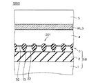
<L−1.装置構成>
本発明に係る半導体装置の実施の形態12として、図41に半導体装置3000の構成を示す。
【0284】
図41に示す半導体装置3000は、図68を用いて説明した半導体装置90を例に採れば、RF回路部91およびロジック部92の一部分を示しており、それぞれRF回路部RPおよびロジック部LPとして示す。
【0285】
図41において、シリコン基板1と、該シリコン基板1上に配設された埋め込み酸化膜2と、埋め込み酸化膜2上に配設されたSOI層3とで構成されるSOI基板SB上に、RF回路部RPおよびロジック部LPが配設されている。
【0286】
RF回路部RPにおいては、SOI層3のスパイラルインダクタSI(平面構成は図70参照)の配設領域に対応する領域が複数のトレンチ分離酸化膜13によって分割され、複数のSOI領域22が形成されている。そして、各SOI領域22の上部にはシリサイド膜32が配設され、それぞれ複数のトレンチ分離酸化膜13、SOI領域22、シリサイド膜32によってPGシールド102が構成されている。
【0287】
そして、PGシールド102の下部のシリコン基板1の内部には空洞部CVが配設されている。
【0288】
空洞部CVはスパイラルインダクタSIの平面方向の長さと同程度の深さ(最大で100μm程度)を有し、平面方向の広がりは、少なくともスパイラルインダクタSIの形成領域を含むように設定されている。
【0289】
そして、埋め込み酸化膜2、SOI層3、層間絶縁膜4および5、スパイラルインダクタSIを覆う絶縁膜6を貫通して空洞部CVに達する開口部OPが配設されている。
【0290】
なお、その他、図8を用いて説明した半導体装置200と同じ構成については同じ符号を付し、説明は省略する。
【0291】
空洞部CVの形成方法は、空洞部CV以外の絶縁膜6までの構成をSOI基板SB上に形成した後、シリコン基板1に達する開口部OPを形成し、例えばKOH(水酸化カリウム)の20%溶液を開口部OPから注入し、シリコン基板1をエッチングする方法を採ることができる。また、下部OPは最終的には絶縁膜等で埋め込まれる。
【0292】
なお、エッチング溶液としてはKOH溶液に限定されるものではなく、シリコン基板のみを溶かす溶液であれば他の溶液でも良い。例えばNaOHなどの強アルカリ溶液も使用可能である。このような溶液は、カリウム(K)やナトリウム(Na)の汚染に注意する必要があるが、単純な物質であるので扱いやすい。また、カテコール(C6H6O2)やTMAH(水酸化テトラメチルアンモニウム:N(CH3)4OH))水溶液などの有機物質を使用しても良い。どの溶液を用いるかはデバイス製造を行う半導体工場の全体の構成に合わせて選択すれば良い。なお、KOH溶液等のエッチング溶液は温度によってエッチングレートが異なり、KOHの20%溶液は、50℃で100nm/minのエッチングレートを有する。
【0293】
また、空洞部CVはSOI基板SB上に何も形成しない状態で形成しておいても良いし、PGシールド102までを形成した段階で形成しても良く、基本的にはどの段階で形成しても良い。
【0294】
<L−2.作用効果>
以上説明したように、半導体装置3000はPGシールド102の下部のシリコン基板1の内部に空洞部CVを有しているので、スパイラルインダクタによる静電誘導損失をPGシールド102により防止するとともに、PGシールド102の内部で発生する渦電流による電磁誘導損失を被ることがない。また、シリコン基板1内で、スパイラルインダクタSIによる渦電流の発生を防止して、電磁誘導損失を低減することができる。
【0295】
なお、上記説明においてはPGシールド102を用いる構成を示したが、PGシールドの形態はこれに限定されるものではなく、実施の形態1〜9を用いて説明した各種PGシールドを適用できることは言うまでもない。
【0296】
<M.実施の形態13>
以上説明した実施の形態12においては、シリコン基板1の内部に空洞部CVを備えることで、シリコン基板1内での電磁誘導損失を低減する構成について示したが、シリコン基板1内での電磁誘導損失を低減する構成はこれに限定されるものではなく、シリコン基板1内にポーラス層を設けることで渦電流の経路を遮断するようにしても良い。
【0297】
なお、本明細書におけるポーラス層は、多数のホールを有する層という意味だけでなく、多数のトレンチを有する層も意味する。
【0298】
<M−1.装置構成>
以下、本発明に係る半導体装置の実施の形態13として、図42に半導体装置4000の構成を示す。
【0299】
なお、図42において、埋め込み酸化膜2より上部の構成は、図8を用いて説明した半導体装置200と同じであり、同じ構成については同じ符号を付し、説明は省略する。
【0300】
図42において、PGシールド102の下部のシリコン基板1の内部にはポーラス層PRが配設されている。
【0301】
ポーラス層PRは、シリコン基板1の表面から内部にかけてエッチングにより形成された複数のトレンチあるいは複数のホール、あるいは陽極化成法により形成された複数のホールで構成されており、それらの内部は真空に近い状態あるいは絶縁物で埋め込まれた状態となっている。
【0302】
従って、スパイラルインダクタSIによって発生する渦電流は、その経路を遮断され、シリコン基板1内での電磁誘導損失を低減することができる。
【0303】
なお、ポーラス層PRの平面視形状は、ホールの場合は、所定の領域全域に不規則にあるいは規則的に設けるようにすれば良いし、トレンチの場合には、少なくとも1つの方向に延在するトレンチを並列に配設することで渦電流を遮断することができる。
【0304】
なお、上記説明においてはPGシールド102を用いる構成を示したが、PGシールドの形態はこれに限定されるものではなく、実施の形態1〜9を用いて説明した各種PGシールドを適用できることは言うまでもない。
【0305】
<M−2.製造方法>
以下、図43〜図53を用いて、ポーラス層PRを有するSOI基板SBの形成方法について説明する。
【0306】
<M−2−1.エッチング法>
図43〜図46を用いてポーラス層PRをエッチングにより形成する方法を説明する。なお、以下においては明確化のため、エッチングにより形成されたものをポーラス層PR1と呼称し、陽極化成法により形成されたものをポーラス層PR2と呼称する。
【0307】
まず、図43に示すように、シリコン基板1を準備し、シリコン基板1の表面から内部にかけてエッチングにより複数のトレンチTR1(あるいは複数のホール)を形成してポーラス層PR1を構成する。なお、複数のトレンチ(あるいは複数のホール)TR1は、少なくともPGシールド102の下部に対応する領域全域に配設され、その溝幅あるいは直径は10nm〜50nm程度、ポーラス層PR1の厚さは10μm〜100μm程度に設定されている。
【0308】
なお、複数のトレンチ(あるいは複数のホール)TR1の深さ(すなわちポーラス層PR1の厚さ)は、スパイラルインダクタSIの平面方向の長さと同程度にすることが望ましいが、スパイラルインダクタSIの平面方向の長さの10分の1程度の深さであっても、電磁誘導損失の低減効果を得ることができる。
【0309】
次に、図44に示す工程において、シリコン基板1上を覆うように、例えばシリコン酸化膜で絶縁膜ZF1を形成し、ポーラス層PR1を埋め込む。
【0310】
図45に、絶縁膜ZF1を形成した状態のポーラス層PR1の詳細を示す。図45に示すように、絶縁膜ZF1は、ポーラス層PR1を構成するトレンチ(あるいはホール)TR1の内面を覆うように配設されるが、その内部を完全に埋め込むよりも早く開口部を塞ぐようなカバレッジ特性の絶縁膜を使用すれば、トレンチ(あるいはホール)TR1の内部には中空部HLが形成される。
【0311】
この場合、絶縁膜ZF1の形成を真空状態下で行っていれば、中空部HLも真空状態となっており、誘電率が低いので静電誘導損失も低減することができる。
【0312】
なお、トレンチ(あるいはホール)TR1の内部を絶縁膜で埋め込んだ場合であっても、当該絶縁膜として例えばフッ素を含むプラズマ酸化膜(プラズマCVD法により形成されたシリコン酸化膜)等の誘電率が低い絶縁膜を使用することで静電誘導損失を低減することができる。
【0313】
なお、熱酸化を行って熱酸化膜を形成する場合も、上記と同様にトレンチ(あるいはホール)TR1の内部には中空部HLを形成することができる。
【0314】
また、トレンチ(あるいはホール)TR1の内部をシリコン酸化膜等で埋め込んだ場合には、フッ素(F)イオンを注入することで誘電率を下げるようにすれば良い。
【0315】
次に、図46に示す工程において、その主面上に所定厚さの絶縁膜ZF2(例えばシリコン酸化膜)を備えるシリコン基板1Aを準備し、絶縁膜ZF1と絶縁膜ZF2とが対面するように、シリコン基板1Aと1とを貼り合わせる。
【0316】
その後、シリコン基板1AにCMP処理を施して、その厚さを薄くすることで、残ったシリコン基板1AがSOI層3となり、絶縁膜ZF1およびZF2が埋め込み酸化膜2となり、シリコン基板1中にポーラス層PR1を有したSOI基板SBを得ることができる。
【0317】
なお、以上の説明においては、ポーラス層PR1を絶縁膜ZF1で覆うことで、ポーラス層PR1の内部に中空部HLを設ける工程を示したが、以下のような方法で、ポーラス層PR1を構成するトレンチあるいはホールの開口部を塞ぐようにしても良い。
【0318】
すなわち、図47に示すようにシリコン基板1内にトレンチ(あるいはホール)TR1を形成した後、水素雰囲気中で数秒間、温度1000℃以上の熱処理(水素アニール)を行う。すると、ポーラス層PR1の表面エネルギーの極小化によって表面原子の移動度が劇的に高められ、表面の自然酸化に起因してトレンチ(あるいはホール)TR1の開口部が還元除去される(図48)。その結果、トレンチ(あるいはホール)TR1の内部が中空部HLとなり、上面が平滑化されたポーラス層PR1が形成される(図49)。
【0319】
これ以降の工程は図46に示した工程と同様であるが、シリコン基板1の表面には絶縁膜を形成する必要がないので、シリコン基板1Aの絶縁膜ZF2は、シリコン基板1のポーラス層PR1が形成された側の主面と対面するように貼り合わせることになる。
【0320】
<M−2−2.陽極化成法>
次に、図50〜図53を用いてポーラス層PRを陽極化成法により形成する方法を説明する。陽極化成法によるポーラス層の形成については、特許出願番号11−117770の明細書中の図6〜図10に開示されている。
【0321】
以下、その開示内容に基づいて説明すると、対向して配設され、陰極となる上部白金電極と、陽極となる下部白金電極とを有し、内部に化成溶液を満たす化成槽を準備する。
【0322】
次に、ポーラス層PR2を形成する側の主面が上部白金電極に向かうように、シリコン基板1を上部白金電極と下部白金電極との間に配置し、化成槽内にHF溶液を満たす。そして、シリコン基板1に電流を流す。化成条件を、例えば、化成時間30秒、化成電流密度10mA/cm2とすると、シリコン基板1の上面が多孔質化され、シリコン基板1の主面内に、0.2μm程度の膜厚を有するポーラス層PR2が形成される。
【0323】
ポーラス層PR2に形成されるホールは、エッチングで形成されるような直線的な形状ではなく、入り組んだ形状となるが、簡略化のため図50に示すような形状として示す。
【0324】
なお、ポーラス層PR2の厚さは化成時間および化成電流密度によって制御することができ、また、化成溶液の種類を変えることで制御することができる。また、ポーラス層PR2の密度(シリコン部分とホール部分との比に相当する)はHF溶液の濃度によって制御することができる。
【0325】
また、ポーラス層PR2の厚さは、スパイラルインダクタSIの平面方向の長さと同程度にすることが望ましいが、スパイラルインダクタSIの平面方向の長さの10分の1程度の厚さであっても、電磁誘導損失の低減効果を得ることができる。
【0326】
次に、先に説明したように、水素雰囲気中で数秒間、温度1000℃以上の熱処理を行ことで、ホールの開口部を還元除去し、ホールの内部が中空部HLとなり、ポーラス層PR2の上面が平滑化されたシリコン基板1を形成する(図50)。
【0327】
なお、ポーラス層PR2はシリコン基板1内に選択的に形成されているが、これは、後に形成されるスパイラルインダクタSIの形成領域に対応して設けられており、ポーラス層PR2を形成しない領域上にはHF溶液が接触しないようにマスクを形成しておけば良い。なお、ポーラス層PR2をシリコン基板1の全域に渡って配設するようにしても良いことは言うまでもない。
【0328】
なお、ポーラス層PR2をシリコン基板1の全域に渡って配設した構成においては、スパイラルインダクタによる電磁誘導損失だけでなく、配線による電磁誘導損失の低減効果も有することになる。
【0329】
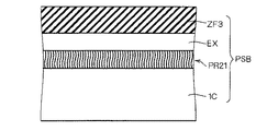
次に、図51に示すように、シリコン基板1C上にポーラス層PR2、エピタキシャル層EX、絶縁膜ZF3が積層されたポーラス基板PSBを準備する。
【0330】
なお、ポーラス基板PSBの形成方法についても、特許出願番号11−117770の明細書中の図6〜図10に開示されている方法を採れば良く、まず、先に説明したポーラス層PR2の形成方法と同様の工程を経て、シリコン基板1Cの内部にポーラス層PR21を形成する。ここで、ポーラス層PR21の上面は、シリコン基板1Cの単結晶構造を維持しており、シリコン基板1Cと同様の結晶方位を有している。そこで次に、エピタキシャル成長法によって、ポーラス層PR21の主面上に、所定厚さのエピタキシャル層EXを形成する。なお、エピタキシャル層EXは後にSOI層3となるので、SOI層3の厚さと同等の厚さに形成される。
【0331】
その後、エピタキシャル層EX上に所定厚さの絶縁膜ZF3を、例えばシリコン酸化膜で形成する。なお、絶縁膜ZF3は後に埋め込み酸化膜2となるので、埋め込み酸化膜2の厚さと同等の厚さに形成される。
【0332】
次に、図52に示す工程において、シリコン基板1のポーラス層PR2が形成された側の主面と、ポーラス基板PSBの絶縁膜ZF3とが対面するように、シリコン基板1とポーラス基板PSBとを貼り合わせる。
【0333】
その後、図53に示すように、ポーラス基板PSBのポーラス層PR21を境界として、ポーラス層PR21およびシリコン基板1Cを剥離するか、あるいは、エピタキシャル層EXの上面までをCMP処理により研磨することで、シリコン基板1内にポーラス層PR2を有するSOI基板SBを得ることができる。
【0334】
<M−3.作用効果>
以上説明したように、図42に示す半導体装置4000においては、スパイラルインダクタによる静電誘導損失をPGシールド102により防止するとともに、PGシールド102の内部で発生する渦電流による電磁誘導損失を被ることがない。また、シリコン基板1内に形成されたポーラス層PRを有し、その内部は真空に近い状態あるいは絶縁物で埋め込まれた状態となっているので、スパイラルインダクタSIによって発生する渦電流は、その経路を遮断され、シリコン基板1内での電磁誘導損失を低減することができる。
【0335】
<M−4.変形例>
以上説明した半導体装置4000のポーラス層PRの形成方法においては、ポーラス層PRを備えたSOI基板SBを準備し、その上に、PGシールド102を始めとする構成を形成する例を示したが、以下、図54を用いて説明するような製造方法を採用しても良い。
【0336】
図54に示すように、SOI層3上にトレンチ分離酸化膜PTI等の構成を形成したSOI基板SBを準備する。なお、SOI層3においては、トレンチ分離酸化膜PTIだけでなく、MOSトランジスタ等が構成された状態であっても良い。
【0337】
そして、SOI基板SBの、スパイラルインダクタの配設領域に対応する領域のSOI層3および埋め込み酸化膜2を選択的に除去して開口部OP1を形成する。
【0338】
その後、ポーラス層PR2を形成する領域のシリコン基板1が露出し、開口部OP1の端縁部およびSOI層3上が覆われるようにレジストマスクRM4を形成する。
【0339】
レジストマスクRM4を形成したSOI基板SBを、上部白金電極UEと、陽下部白金電極LEとを有する化成槽CC内に配設し、化成槽内にHF溶液を満たして上部白金電極UEと陽下部白金電極LEとの間に電流を流すことで、シリコン基板1の露出部分にポーラス層PR2が形成される。
【0340】
ポーラス層PR2の形成後にレジストマスクRM4を除去し、開口部OP1内に絶縁膜を形成して埋め込み酸化膜2を修復し、さらに当該絶縁膜上にシリコン層を形成してSOI層3を修復し、SOI層3内にPGシールド102を形成することで半導体装置4000と同様の構成を形成すれば良い。
【0341】
なお、実施の形態1〜10において説明した各種PGシールドを使用しない場合には、単に、開口部OP1を絶縁膜で埋め込むだけでも良い。
【0342】
<N.実施の形態14>
以上説明した実施の形態13においては、SOI基板SBのシリコン基板1内にポーラス層PRを有する構成について示したが、SOI基板のSOI層内にポーラス層を有した構成であっても良い。
【0343】
<N−1.装置構成>
以下、本発明に係る半導体装置の実施の形態14として、図55に半導体装置5000の構成を示す。
【0344】
図55においては、シリコン基板1と、該シリコン基板1上に配設された埋め込み酸化膜2Aと、埋め込み酸化膜2A上に配設されたSOI層3Aとで構成されるSOI基板SBA上に配設されたRF回路部を示している。
【0345】
スパイラルインダクタSI(平面構成は図70参照)の配設領域に対応するSOI層3A内に、互いに密接したSOI領域251〜257で構成されるPGシールド105が形成されている。なお、PGシールド105の構成は図18を用いて説明した半導体装置500と同一であり、さらにSOI領域258および259を有しているが、図においては省略している。
【0346】
そして、PGシールド105上は部分分離酸化膜であるトレンチ分離酸化膜17で覆われている。
【0347】
また、トレンチ分離酸化膜17に隣接してMOSトランジスタQ40が形成されている。MOSトランジスタQ40はトレンチ分離酸化膜17で規定されるSOI領域80上に配設されたゲート絶縁膜GZ、ゲート絶縁膜GZ上に配設されたゲート電極GT、ゲート電極GT上に配設されたシリサイド膜GSおよび、それらの側面を覆うように配設されたサイドウォール絶縁膜GW1およびGW2を備えている。
【0348】
ここで、サイドウォール絶縁膜GW2が形成される側のソース・ドレイン領域SD2は、反対側のソース・ドレイン領域SD1よりも広く形成され、サイドウォール絶縁膜GW2はソース・ドレイン領域SD2上に延在している。
【0349】
そして、サイドウォール絶縁膜GW1の外側のソース・ドレイン領域SD1の表面内にはシリサイド膜SS1が配設され、サイドウォール絶縁膜GW2の外側のソース・ドレイン領域SD2の表面内にはシリサイド膜SS2が配設されており、結果として、ゲート電極GTがソース・ドレイン領域SD1寄りに配設され、いわゆるオフセットゲートとなっている。オフセットゲートはドレイン領域での電界集中を緩和し、MOSトランジスタの高耐圧化を図ることができるので、電力用半導体装置に適した構造である。
【0350】
なお、シリサイド膜SS1およびSS2は、コンタクト部CP5およびCP6によって上層の配線WL5およびWL6に接続されている。
【0351】
なお、その他、図18を用いて説明した半導体装置500と同一の構成については同一の符号を付し、重複する説明は省略する。
【0352】
そして、図55に示すように、SOI層3Aの内部にはポーラス層PR3が配設されている。
【0353】
ポーラス層PR3は、シリコン基板1の表面から内部にかけて陽極化成法により形成された複数のホールで構成されており、それらの内部は真空に近い状態、あるいは絶縁物で埋め込まれた状態となっている。
【0354】
従って、スパイラルインダクタSIによって発生する渦電流は、その経路を遮断され、SOI層3A内での電磁誘導損失を低減することができる。
【0355】
<N−2.製造方法>
以下、図56〜図59を用いて、ポーラス層PR3をSOI層内に有するSOI基板SBAの形成方法について説明する。
【0356】
ポーラス層をSOI層内に有するSOI基板の形成方法については、特許出願番号11−165951の明細書中の図1〜図9に開示されている。
【0357】
以下、その開示内容に基づいて説明すると、まず、図56に示す工程において、シリコン基板1Dの主面内に、厚さ1μm程度のポーラス層PR3を陽極化成法により形成する。なお、ポーラス層PR3形成後、先に説明したように、水素雰囲気中で数秒間、温度1000℃以上の熱処理を行ことで、ホールの開口部を還元除去してホールの内部を中空部とし、ポーラス層PR3の上面を平滑化しても良いことは言うまでもない。
【0358】
また、陽極化成法の代わりに、エッチングによりに複数のトレンチ(あるいはホール)を形成してポーラス層PR3を構成しても良い。
【0359】
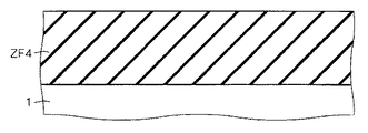
次に、図57に示すように、その主面上に所定厚さの絶縁膜ZF4が形成されたシリコン基板1を準備する。なお、絶縁膜ZF4は後に埋め込み酸化膜2Aとなるので、埋め込み酸化膜2Aの厚さと同等の厚さに形成される。
【0360】
そして、図58に示す工程において、シリコン基板1Dのポーラス層PR3が形成された側の主面と、シリコン基板1の絶縁膜ZF4とが対面するように、シリコン基板1と1Dとを貼り合わせる。
【0361】
その後、図59に示すように、シリコン基板1DをCMP処理により研磨してその厚みを減らし、ポーラス層PR3と合わせてSOI層3Aの厚さと同等の厚さに形成することで、SOI層3A内にポーラス層PR3を有するSOI基板SBAを得ることができる。
【0362】
なお、SOI基板SBAの形成方法は上記方法に限定されるものではなく、特許出願番号11−165951の明細書中の図10〜図19に開示された方法を用いても良い。
【0363】
すなわち、第1のシリコン基板に第1のポーラス層を形成し、その上にエピタキシャル成長法によって、所定厚さのエピタキシャル層を形成する。その後、エピタキシャル層の主面内に第2のポーラス層を形成し、第2のポーラス層上にシリコン酸化膜を形成してこれを第1の基板とする。
【0364】
その後、第2の基板として第2のシリコン基板を別途準備し、第1の基板のシリコン酸化膜と、第2の基板の主面とが対面するように両者を貼り合わせる。
【0365】
そして、第1のポーラス層を境として、第1のポーラス層および第1のシリコン基板を剥離することで、第2のシリコン基板、シリコン酸化膜、第2のポーラス層、エピタキシャル層が積層されたSOI基板を得ることができる。
【0366】
<N−3.作用効果>
以上説明したように、図55に示す半導体装置5000においては、スパイラルインダクタによる静電誘導損失をPGシールド105により防止するとともに、PGシールド105の内部で発生する渦電流に起因する電磁誘導損失を被ることがない。また、SOI層3A内に形成されたポーラス層PR3を有し、その内部は真空に近い状態あるいは絶縁物で埋め込まれた状態となっているので、スパイラルインダクタSIによって発生する渦電流は、その経路を遮断され、SOI層3A内での電磁誘導損失を低減することができる。
【0367】
<O.実施の形態15>
以上説明した実施の形態12〜14においては、SOI基板上に形成された半導体装置において、シリコン基板内あるいはSOI層内にポーラス層を有し、シリコン基板内およびSOI層内でのスパイラルインダクタおよび配線による電磁誘導損失を防止する構成について説明したが、本発明の適用はSOI基板に限定されるものではなく、バルク基板と呼称されるシリコン基板に適用することもできる。
【0368】
<O−1.装置構成>
本発明に係る半導体装置の実施の形態15として、図60に半導体装置6000の構成を示す。なお、図60に示す半導体装置6000は、図68を用いて説明した半導体装置90を例に採れば、RF回路部RPおよびロジック部LPの構成を示している。
【0369】
図60において、P型のシリコン基板1のスパイラルインダクタSI(平面構成は図70参照)の配設領域に対応する領域が複数のトレンチ分離酸化膜111によって分割され、P型不純物が比較的高濃度(P+)に注入された複数の不純物領域121が形成されている。トレンチ分離酸化膜111は、シリコン基板1の表面から所定深さに達するように配設されたトレンチ内にシリコン酸化膜を埋め込むことで形成されている。
【0370】
また、各不純物領域121の上部にはシリサイド膜131が配設され、それぞれ複数のトレンチ分離酸化膜111、不純物領域121、シリサイド膜131によって、PGシールド301が構成される。
【0371】
ロジック部LPにおいては、トレンチ分離酸化膜15によってSOI層3が分割され、SOI領域61および62が形成され、SOI領域61および62にはMOSトランジスタQ21およびQ22がそれぞれ形成されている。
【0372】
なお、不純物領域121以下のシリコン基板1の内部にはN型不純物が比較的低濃度(N-)に注入されたウエル領域NWがシリコン基板1全域に渡って形成されているとともに、ウエル領域NWを含めて不純物領域121以下のシリコン基板1の内部には所定厚さのポーラス層PR4がシリコン基板1全域に渡って形成されている。
【0373】
その他、図8に示した半導体装置200と同一の構成については同一の符号を付し、重複する説明は省略する。
【0374】
<O−2.作用効果>
以上説明したように、図60に示す半導体装置6000においては、スパイラルインダクタによる静電誘導損失をPGシールド301により防止するとともに、PGシールド301の内部で発生する渦電流に起因する電磁誘導損失を被ることがない。また、シリコン基板1内に形成されたポーラス層PR4を有し、その内部は真空に近い状態となっているので、スパイラルインダクタSIによって発生する渦電流は、その経路を遮断され、シリコン基板1内での電磁誘導損失を低減することができる。
【0375】
また、ポーラス層PR4はシリコン基板1の全域に渡って配設されているので、スパイラルインダクタによる電磁誘導損失だけでなく、配線による電磁誘導損失の低減効果も有することになる。
【0376】
<P.実施の形態16>
以上説明した実施の形態12〜15においては、SOI基板上あるいはバルクシリコン基板上に形成された半導体装置において、シリコン基板内あるいはSOI層内にポーラス層を有し、シリコン基板内およびSOI層内でのスパイラルインダクタおよび配線による電磁誘導損失を防止する構成について説明したが、実施の形態1〜10において説明した各種PGシールドをさらに改良した以下に説明する構成により、シリコン基板内およびSOI層内での電磁誘導損失を防止することができる。
【0377】
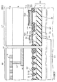
<P−1.装置構成>
本発明に係る半導体装置の実施の形態16として、図61に半導体装置7000の構成を示す。なお、図61に示す半導体装置7000は、図68を用いて説明した半導体装置90を例に採れば、RF回路部RPおよびロジック部LPの構成を示している。
【0378】
図61において、シリコン基板1と、該シリコン基板1上に配設された埋め込み酸化膜2と、埋め込み酸化膜2上に配設されたSOI層3とで構成されるSOI基板SB上に、RF回路部RPおよびロジック部LPが配設されている。
【0379】
RF回路部RPにおいては、SOI層3のスパイラルインダクタSI(平面構成は図70参照)の配設領域に対応する領域が複数のトレンチ分離酸化膜13によって分割され、複数のSOI領域22が形成されている。トレンチ分離酸化膜13は、SOI層3の表面から埋め込み酸化膜2の表面に達するように配設されたトレンチ内にシリコン酸化膜を埋め込むことで形成され、各SOI領域22は電気的に完全に分離されている。
【0380】
また、各SOI領域22の上部にはシリサイド膜32が配設され、それぞれ複数のトレンチ分離酸化膜13、SOI領域22、シリサイド膜32によって、PGシールド102が構成される。
【0381】
ロジック部LPにおいては、トレンチ分離酸化膜15によってSOI層3が分割され、SOI領域61および62が形成され、SOI領域61および62にはMOSトランジスタQ21およびQ22がそれぞれ形成されている。
【0382】
そして、それぞれのトレンチ分離酸化膜13の下部には、トレンチ分離酸化膜13で開口部が塞がれたトレンチTR3が配設されている。
【0383】
トレンチTR3は埋め込み酸化膜2を貫通してシリコン基板1の内部に達し、その深さは100μm程度となっている。
【0384】
また、トレンチ分離酸化膜13で開口部が塞がれたトレンチTR3の内部には中空部HLが形成されている。
【0385】
その他、図8に示した半導体装置200と同一の構成については同一の符号を付し、重複する説明は省略する。
【0386】
<P−2.製造方法>
以下、図62〜図64を用いてPGシールド102およびトレンチTR3の製造方法について説明する。
【0387】
まず、図9を用いて説明した半導体装置200の製造方法と同様に、SOI層3上に厚さ20nm程度のシリコン酸化膜OXおよび厚さ200nm程度のシリコン窒化膜SNを順次形成した後、パターニングによりシリコン酸化膜OX、シリコン窒化膜SNおよびSOI層3の多層膜を、SOI層3の下層部が残るようにエッチングし、トレンチ分離酸化膜13、14および15が形成される領域にトレンチTR131、TR141およびTR15を形成する。
【0388】
次に、図62に示す工程において、トレンチTR131、TR141の一部を覆うとともに、トレンチTR15を完全に覆うレジストマスクRM2を用いて、トレンチTR131、TR141のレジストマスクRM2で覆われない部分をさらにエッチングすることによりSOI層3を貫通するトレンチTR13およびTR14を形成する。
【0389】
次に、レジストマスクRM2を除去した後、図63に示す工程において、トレンチTR13部分が開口部となるようにパターニングされたレジストマスクRM21を用いて、埋め込み酸化膜2を貫通してシリコン基板1の内部に達する深さ100μm程度のトレンチTR3を形成する。
【0390】
次に、レジストマスクRM21を除去した後、図64に示す工程において、全面に渡って、トレンチTR3の溝幅(例えば200nm〜500nm)よりも厚い、例えば厚さ500nm程度のシリコン酸化膜ZF5を形成して、トレンチTR13〜TR15およびトレンチTR3を埋め込み、CMP(Chemical Mechanical Polishing)処理によりシリコン窒化膜SNの途中まで研磨し、その後、シリコン窒化膜SNおよびシリコン酸化膜OXを除去することで、トレンチ分離酸化膜13〜15およびトレンチ分離酸化膜13で覆われたトレンチTR13を得る。
【0391】
シリコン酸化膜ZF5は、トレンチTR13の内面を覆うように配設されるが、その内部を完全に埋め込むよりも早く開口部を塞ぐようなカバレッジ特性の絶縁膜を使用すれば、トレンチTR3の内部には中空部HLが形成される。
【0392】
この場合、絶縁膜ZF5の形成を真空状態下で行っていれば、中空部HLも真空状態となっており、誘電率が低いので静電誘導損失も低減することができる。
【0393】
なお、この後は、既存のMOSトランジスタの製造工程(既存のサリサイド工程を含む)、層間絶縁膜の製造工程、配線層の製造工程、スパイラルインダクタの製造工程等を経て、半導体装置7000を得る。
【0394】
なお、PGシールド102の平面視形状は、例えば図2を用いて説明した形状を採用しても良いし、図3〜図7を用いて説明した形状を採用しても良く、トレンチTR3の平面視形状は、各PGシールドのトレンチ分離酸化膜の形状に相似した形状となる。
【0395】
<P−3.作用効果>
以上説明したように、図61に示す半導体装置7000においては、スパイラルインダクタによる静電誘導損失をPGシールド102により防止するとともに、PGシールド102の内部で発生する渦電流による電磁誘導損失を被ることがない。また、トレンチ分離酸化膜13の下部に配設され、埋め込み酸化膜2を貫通してシリコン基板1の内部に達するトレンチTR3によって、スパイラルインダクタSIによって発生する渦電流の経路が遮断され、シリコン基板1内での電磁誘導損失を低減することができる。
【0396】
<P−4.変形例1>
以上説明した半導体装置7000においては、PGシールド102を構成するトレンチ分離酸化膜13の下部に埋め込み酸化膜2を貫通してシリコン基板1の内部に達するトレンチTR3を設けた構成を示したが、図65に示す半導体装置8000のように、PGシールド101を構成するトレンチ分離酸化膜11の下部に、埋め込み酸化膜2を貫通してシリコン基板1の内部に達するトレンチTR4を設けるようにしても良い。
【0397】
トレンチTR4の深さは100μm程度となっており、レンチ分離酸化膜11で開口部が塞がれたトレンチTR4の内部には中空部HLが形成されている。
【0398】
その他、図1に示した半導体装置100と同一の構成については同一の符号を付し、重複する説明は省略する。
【0399】
<P−5.変形例2>
また、図66に示す半導体装置9000のように、PGシールド103Aを構成するトレンチ分離酸化膜16の下部に、埋め込み酸化膜2を貫通してシリコン基板1の内部に達するトレンチTR5を設けるようにしても良い。
【0400】
トレンチTR5の深さは100μm程度となっており、レンチ分離酸化膜16で開口部が塞がれたトレンチTR5の内部には中空部HLが形成されている。
【0401】
その他、図14に示した半導体装置300Aと同一の構成については同一の符号を付し、重複する説明は省略する。
【0402】
<P−6.変形例3>
また、図67に示す半導体装置8001のように、P型のシリコン基板1のスパイラルインダクタSI(平面構成は図70参照)の配設領域に対応して形成されたPGシールド301を構成するトレンチ分離酸化膜111の下部に、所定深さのトレンチTR6を設けるようにしても良い。
【0403】
トレンチTR6の深さは100μm程度となっており、レンチ分離酸化膜111で開口部が塞がれたトレンチTR6の内部には中空部HLが形成されている。
【0404】
その他、図40に示した半導体装置2000と同一の構成については同一の符号を付し、重複する説明は省略する。
【0405】
【発明の効果】
本発明に係る請求項1記載の半導体装置によれば、接地電位に接続された少なくとも1つの導電部と、少なくとも1つの導電部の平面内に、例えばスパイラルインダクタ等のインダクタンス素子によって誘起される渦電流の経路を遮断する少なくとも1つの電流遮断部とを有するシールド層を半導体基板の主面内に備えているので、静電誘導損失を低減できるとともに、シールド層内での渦電流の経路遮断され、電磁誘導損失をも低減できる。また、シールド層が半導体基板内に形成されるので、シールド層を例えばMOSトランジスタの形成工程で同時に形成することにより、シールド層の形成のために新たな導体層は不要であり、装置構造が複雑になることもない。また、少なくとも1つの電流遮断部が埋め込み酸化膜に達する複数の分離酸化膜で構成され、少なくとも1つの導電部が、複数の分離酸化膜で電気的に分離された複数のSOI領域で構成されるので、複数のSOI領域を通じて電流が流れ、静電誘導損失を低減できるとともに、渦電流の経路が分離酸化膜により遮断されるので、渦電流による電磁誘導損失を被ることがない。
【0407】
本発明に係る請求項2記載の半導体装置によれば、複数の分離酸化膜のそれぞれが、所定の形成幅で、埋め込み酸化膜に延在する形状であり、いわゆる完全分離酸化膜の形状であるので、例えばMOSトランジスタの形成部において完全分離酸化膜を用いて素子分離を行う場合に、同時に形成することができ、製造方法が複雑になることがない。
【0408】
本発明に係る請求項3記載の半導体装置によれば、複数の分離酸化膜のそれぞれは、第1の形成幅で埋め込み酸化膜上に延在する第1の部分と、第1の部分の下部に連続し、第1の形成幅よりも狭い第2の形成幅で埋め込み酸化膜の表面に延在する第2の部分とで構成される形状であり、いわゆる部分分離酸化膜の製造工程を経て形成されるので、例えばMOSトランジスタの形成部において部分分離酸化膜を用いて素子分離を行う場合に、同時に形成することができ、製造方法が複雑になることがない。
【0409】
本発明に係る請求項4記載の半導体装置によれば、少なくとも1つの導電部が、SOI層を薄くして所定厚さとなった複数のSOI領域で構成され、少なくとも1つの電流遮断部が、複数のSOI領域の間を埋めるように配設された絶縁膜で構成されているので、複数のSOI領域を通じて電流が流れ、静電誘導損失を低減できるとともに、渦電流の経路が絶縁膜により遮断されるので、渦電流による電磁誘導損失を被ることがない。また、少なくとも1つの導電部はSOI層を分割して形成されるので、シールド層の形成のために新たな導体層は不要であり、装置構造が複雑になることもない。
【0410】
本発明に係る請求項5記載の半導体装置によれば、インダクタンス素子の下の複数のSOI領域のそれぞれが、インダクタンス素子が上にない領域のSOI領域より半導体不純物を高濃度に有するので、抵抗値の低いSOI領域を得ることができる。
【0411】
本発明に係る請求項6記載の半導体装置によれば、複数のSOI領域のそれぞれが、その上面にシリサイド膜を有するので、抵抗値の低いSOI領域を得ることができる。
【図面の簡単な説明】
【図1】 本発明に係る実施の形態1の半導体装置の構成を示す断面図である。
【図2】 本発明に係る実施の形態1の半導体装置のPGシールドの平面構成を示す図である。
【図3】 PGシールドの他の平面構成を示す図である。
【図4】 PGシールドの他の平面構成を示す図である。
【図5】 PGシールドの他の平面構成を示す図である。
【図6】 PGシールドの他の平面構成を示す図である。
【図7】 PGシールドの他の平面構成を示す図である。
【図8】 本発明に係る実施の形態2の半導体装置の構成を示す断面図である。
【図9】 本発明に係る実施の形態2の半導体装置の製造工程を示す断面図である。
【図10】 本発明に係る実施の形態2の半導体装置の製造工程を示す断面図である。
【図11】 本発明に係る実施の形態2の半導体装置の製造工程を示す断面図である。
【図12】 本発明に係る実施の形態3の半導体装置の構成を示す断面図である。
【図13】 本発明に係る実施の形態3の半導体装置の構成を示す断面図である。
【図14】 本発明に係る実施の形態3の半導体装置の変形例の構成を示す断面図である。
【図15】 本発明に係る実施の形態4の半導体装置の構成を示す断面図である。
【図16】 本発明に係る実施の形態4の半導体装置のPGシールドの平面構成を示す図である。
【図17】 本発明に係る実施の形態4の半導体装置の変形例の構成を示す断面図である。
【図18】 本発明に係る実施の形態5の半導体装置の構成を示す断面図である。
【図19】 ディッシングを説明する図である。
【図20】 本発明に係る実施の形態6の半導体装置の構成を示す断面図である。
【図21】 本発明に係る実施の形態6の半導体装置のPGシールドの平面構成を示す図である。
【図22】 本発明に係る実施の形態6の半導体装置の変形例の構成を示す断面図である。
【図23】 本発明に係る実施の形態6の半導体装置の変形例のPGシールドの平面構成を示す図である。
【図24】 本発明に係る実施の形態7の半導体装置の構成を示す断面図である。
【図25】 本発明に係る実施の形態7の半導体装置のPGシールドの平面構成を示す図である。
【図26】 本発明に係る実施の形態7の半導体装置の変形例の構成を示す断面図である。
【図27】 本発明に係る実施の形態7の半導体装置の変形例の構成を示す断面図である。
【図28】 本発明に係る実施の形態7の半導体装置の変形例の構成を示す断面図である。
【図29】 本発明に係る実施の形態8の半導体装置の構成を示す断面図である。
【図30】 本発明に係る実施の形態8の半導体装置のPGシールドの平面構成を示す図である。
【図31】 本発明に係る実施の形態8の半導体装置の変形例の構成を示す断面図である。
【図32】 本発明に係る実施の形態8の半導体装置の変形例のPGシールドの平面構成を示す図である。
【図33】 本発明に係る実施の形態9の半導体装置の構成を示す断面図である。
【図34】 本発明に係る実施の形態9の半導体装置のPGシールドの平面構成を示す図である。
【図35】 本発明に係る実施の形態9の半導体装置の製造工程を示す断面図である。
【図36】 本発明に係る実施の形態9の半導体装置の変形例の構成を示す断面図である。
【図37】 本発明に係る実施の形態10の半導体装置の構成を示す斜視図である。
【図38】 本発明に係る実施の形態10の半導体装置の構成を示す断面図である。
【図39】 本発明に係る実施の形態10の半導体装置の変形例の構成を示す断面図である。
【図40】 本発明に係る実施の形態11の半導体装置の構成を示す断面図である。
【図41】 本発明に係る実施の形態12の半導体装置の構成を示す断面図である。
【図42】 本発明に係る実施の形態13の半導体装置の構成を示す断面図である。
【図43】 本発明に係る実施の形態13の半導体装置の製造工程を示す断面図である。
【図44】 本発明に係る実施の形態13の半導体装置の製造工程を示す断面図である。
【図45】 本発明に係る実施の形態13の半導体装置の製造工程を示す断面図である。
【図46】 本発明に係る実施の形態13の半導体装置の製造工程を示す断面図である。
【図47】 水素アニールによりポーラス層に中空部を設ける工程を示す断面図である。
【図48】 水素アニールによりポーラス層に中空部を設ける工程を示す断面図である。
【図49】 水素アニールによりポーラス層に中空部を設ける工程を示す断面図である。
【図50】 ポーラス層を陽極化成法により形成する工程を示す断面図である。
【図51】 ポーラス層を陽極化成法により形成する工程を示す断面図である。
【図52】 ポーラス層を陽極化成法により形成する工程を示す断面図である。
【図53】 ポーラス層を陽極化成法により形成する工程を示す断面図である。
【図54】 ポーラス層を陽極化成法により形成する他の方法を示す断面図である。
【図55】 本発明に係る実施の形態14の半導体装置の構成を示す断面図である。
【図56】 本発明に係る実施の形態14の半導体装置の製造工程を示す断面図である。
【図57】 本発明に係る実施の形態14の半導体装置の製造工程を示す断面図である。
【図58】 本発明に係る実施の形態14の半導体装置の製造工程を示す断面図である。
【図59】 本発明に係る実施の形態14の半導体装置の製造工程を示す断面図である。
【図60】 本発明に係る実施の形態15の半導体装置の構成を示す断面図である。
【図61】 本発明に係る実施の形態16の半導体装置の構成を示す断面図である。
【図62】 本発明に係る実施の形態16の半導体装置の製造工程を示す断面図である。
【図63】 本発明に係る実施の形態16の半導体装置の製造工程を示す断面図である。
【図64】 本発明に係る実施の形態16の半導体装置の製造工程を示す断面図である。
【図65】 本発明に係る実施の形態16の半導体装置の変形例の構成を示す断面図である。
【図66】 本発明に係る実施の形態16の半導体装置の変形例の構成を示す断面図である。
【図67】 本発明に係る実施の形態16の半導体装置の変形例の構成を示す断面図である。
【図68】 高周波回路を備えた半導体装置の構成例を示すブロック図である。
【図69】 インダクタによる静電誘導損失を説明する図である。
【図70】 スパイラルインダクタおよびシールドプレートの構成を示す斜視図である。
【図71】 パーフォレーテイッドシールドの構成を示す図である。
【符号の説明】
2 埋め込み酸化膜、2 SOI層、11,13,16〜19 トレンチ分離酸化膜、21,22,23,241〜249,261〜269,271〜279,281〜289,291〜299 SOI領域、31,32,34 シリサイド膜、SB SOI基板、SI スパイラルインダクタ、101〜108,106A,107A,107B,107C,108A,109A,201,301 PGシールド、CV 空洞部、PR,PR1,PR2,PR3,PR4 ポーラス層、TR3,TR4,TR5,TR6 トレンチ。[0001]
BACKGROUND OF THE INVENTION
The present invention relates to a semiconductor device.In placeIn particular, the present invention relates to a semiconductor device including a high frequency circuit having an inductor.
[0002]
[Prior art]
An example of a structure of a semiconductor device provided with a high-frequency circuit is described with reference to FIG. FIG. 68 is a block diagram showing a configuration of a
[0003]
As shown in FIG. 68, the
[0004]
A so-called high-frequency circuit including the
[0005]
68 shows the inductor L1 in the
[0006]
A configuration for preventing such electrostatic induction loss is shown in FIG. In FIG. 69, the parasitic capacitor C1 is not only grounded via the resistor R1, but also grounded via the resistor R2. The resistance value of the resistor R2 is set to be extremely lower than that of the resistor R1, and the high-frequency current mainly flows to the ground via the resistor R2 and does not cause electrostatic induction loss.
[0007]
Note that the end A of the inductor L1 is connected to the
[0008]
The resistor R2 is a conductor plate called a shield plate, and is disposed below the inductor L1. FIG. 70 is a perspective view showing the configurations of the inductor L1 and the shield plate.
[0009]
As shown in FIG. 70, the inductor L1 is formed by winding a wire in a spiral shape, and will be referred to as a spiral inductor SI in the following description. The central part of the vortex, which is one end of the spiral inductor SI, is connected to the lower layer wiring WL via a contact part CP that penetrates an interlayer insulating film (not shown). The wiring WL is disposed on the interlayer insulating film SZ that covers the semiconductor substrate SB.
[0010]
Note that the wiring WL corresponds to the end B of the inductor L1 shown in FIG. 69, and the end A corresponds to the other end of the spiral inductor SI.
[0011]
The semiconductor substrate SB is an SOI (silicon on insulator) substrate, and FIG. 70 shows only the SOI layer SL and the element isolation oxide film FZ disposed in the SOI layer SL. On the element isolation oxide film FZ, a plate-shaped shield plate SP having an area at least equivalent to the arrangement area in the planar direction of the spiral inductor SI is arranged at a position corresponding to the formation region of the spiral inductor SI.
[0012]
The shield plate SP is made of a low-resistance conductor similar to the wiring material, and is grounded via a wiring (not shown), so that no electrostatic induction loss occurs.
[0013]
However, an eddy current is generated inside the shield plate SP due to the current flowing through the spiral inductor SI, and electromagnetic induction loss increases. Therefore, there is a new problem that total power loss increases.
[0014]
In order to solve this problem, a perforated ground shield (hereinafter referred to as a PG shield) has been proposed in which a shield plate is cut out at various points so as to block an eddy current path.
[0015]
FIG. 71 shows an example of a PG shield. The PG shield shown in FIG. 71 is composed of a plurality of plates PL, and the plates PL are electrically insulated. The planar shape of the plate PL is a triangle, and each of the apexes is arranged radially so as to constitute the central portion of the PG shield.
[0016]
By adopting such a configuration, the eddy current path is interrupted and electromagnetic induction loss can be reduced.
[0017]
[Problems to be solved by the invention]
As described above, in the conventional semiconductor device having the inductor, the electrostatic induction loss and the electromagnetic induction loss are reduced by using the PG shield. To form the PG shield, the conductor layer is increased by one layer. There is a problem that the structure is complicated and the manufacturing process is increased.
[0018]
The present invention has been made to solve the above-described problems. In a semiconductor device having an inductor, electrostatic induction loss and electromagnetic induction loss can be reduced, and the structure and manufacturing process become complicated. An object of the present invention is to provide a semiconductor device that prevents the above.
[0019]
[Means for Solving the Problems]
According to a first aspect of the present invention, there is provided a semiconductor device comprising: a semiconductor substrate; a shield layer disposed within a main surface of the semiconductor substrate; and an interlayer insulating film interposed between the shield layer formation regions. The shield layer has at least one conductive part connected to a ground potential and at least one current blocking part in a plane of the at least one conductive part.Andin frontThe semiconductor substrate is an SOI substrate comprising a substrate portion serving as a base, a buried oxide film disposed on the substrate portion, and an SOI layer disposed on the buried oxide film. The current interrupting portion includes a plurality of selectively separated oxide films that penetrate the SOI layer from the surface of the SOI layer and reach the buried oxide film, and the at least one conductive portion includes the plurality of conductive portions. Including a plurality of SOI regions electrically isolated by an isolation oxide filmYes.
[0021]
Claims related to the present invention2In the described semiconductor device, each of the plurality of isolation oxide films has a predetermined formation width and the surface of the buried oxide film.Extended to the surfaceExist.
[0022]
Claims related to the present invention3In the described semiconductor device, each of the plurality of isolation oxide films has a first formation width and the buried oxide film.aboveA surface of the buried oxide film having a first formation extending and a second formation width that is continuous with a lower portion of the first portion and is narrower than the first formation width.Extended to the surfaceAnd the second part.
[0023]
Claims related to the present invention4The semiconductor device described is an SOI substrate in which the semiconductor substrate includes a base substrate portion, a buried oxide film disposed on the substrate portion, and an SOI layer disposed on the buried oxide film. The at least one conductive portion includes a plurality of SOI regions having a predetermined thickness by thinning the SOI layer, and the at least one current interrupting portion fills at least the plurality of SOI regions. It is arranged.
[0024]
Claims related to the present invention5The semiconductor device described isUnder the inductance elementEach of the plurality of SOI regions isFrom the SOI region where the inductance element is not located aboveSemiconductor impuritiesThe highHave to concentration.
[0025]
Claims related to the present invention6In the described semiconductor device, each of the plurality of SOI regions has a silicide film on the upper surface thereof.
[0058]
DETAILED DESCRIPTION OF THE INVENTION
<
<A-1. Device configuration>
As
[0059]
The
[0060]
In FIG. 1, RF is formed on an SOI substrate SB composed of a
[0061]
In the RF circuit portion RP, a region corresponding to the region where the spiral inductor SI (see FIG. 70 for the planar configuration) of the
[0062]
The trench
[0063]
In addition, a
[0064]
Note that, like the trench
[0065]
Further, the formation region of the
[0066]
MOS transistors Q11 and Q12 are formed in
[0067]
Further, in the MOS transistor Q11, the silicide film SS and the source / drain region SD disposed in the surface of the
[0068]
An interlayer insulating
[0069]
An interlayer insulating
[0070]
Here, the plan view shape of the
[0071]
That is, the plurality of SOI regions 21 are classified into two types of
[0072]
When one set of
[0073]
Since the four
[0074]
The configuration of the
[0075]
<A-2. Effect>
As described above, the
[0076]
An increase in electrostatic induction loss and electromagnetic induction loss reduces the Q value (value obtained by dividing the energy stored in the inductor by various losses), which reduces the electrostatic induction loss and electromagnetic induction loss. This contributes to the improvement of the Q value.
[0077]
The trench
[0078]
Further, since the
[0079]
In the above description, the element isolation using trench isolation is shown, but it goes without saying that other element isolation techniques such as LOCOS (Local Oxide of Silicon) isolation or mesa isolation may be used. Yes. This is the same in the embodiments other than the embodiment for the purpose of solving dishing peculiar to trench isolation among the
[0080]
<A-3. Modification>
The shape of the PG shield in plan view is not limited to the shape shown in FIG.
[0081]
3 to 7 show other examples of the plan view shape of the PG shield.
[0082]
In the PG shield shown in FIG. 3, the two
[0083]
The PG shield shown in FIG. 4 has a configuration in which an SOI region 21B having a rectangular shape in plan view is equal to the entire size of the PG shield and has a notch NP that reaches the central portion thereof. The trench
[0084]
The PG shield shown in FIG. 5 is configured by arranging four
[0085]
The PG shield shown in FIG. 6 has four elongated SOI regions 21D arranged in a row so that the sides in the longitudinal direction are parallel to each other. A trench
[0086]
The PG shield shown in FIG. 7 has three types of L-shaped
[0087]
<B. Second Embodiment>
<B-1. Device configuration>
As
[0088]
The
[0089]
In FIG. 8, on an SOI substrate SB composed of a
[0090]
In the RF circuit portion RP, a region corresponding to the region where the spiral inductor SI (see FIG. 70 for the planar configuration) of the
[0091]
In addition, a
[0092]
The trench
[0093]
Note that, for example, the shape described with reference to FIG. 2 may be employed as the planar view shape of the
[0094]
Further, the RF circuit portion RP and the logic portion LP are electrically separated by the trench
[0095]
In addition, unlike the trench
[0096]
<B-1-1. About partial isolation oxide film>
Here, the partial isolation oxide film will be briefly described. In a MOS transistor that is electrically completely isolated from other elements by a complete isolation oxide film, latch-up does not occur between other MOS transistors in principle.
[0097]
Therefore, when manufacturing an SOI device having a CMOS transistor using a complete isolation oxide film, there is an advantage that the minimum isolation width determined by the fine processing technique can be used and the chip area can be reduced. However, carriers (holes in NMOS) generated by the impact ionization phenomenon are accumulated in the channel formation region (body region), which causes kinks, deteriorates the operating breakdown voltage, and the channel formation region potential is not stable. For this reason, there is an influence due to the substrate floating effect such as frequency dependency of the delay time.
[0098]
Regarding the fluctuation of the channel formation region potential, see `` IEEE TRANSACTIONS ON ELECTRON DEVICES, VOL.45, NO.7, JULY 1998, pp1479-1484, '' Analysis of Delay Time Instability According to the Operating Frequency in Field Shield Isolated. Specifically described in SOI Circuits “S. Maeda et al.” (Reference 1). That is, since the potential of the body region changes transiently, the characteristics of the transistor also change transiently, and the circuit operation becomes unstable (see FIG. 7 of Document 1).
[0099]
It has also been verified that frequency dependence appears in the delay time as shown in FIG.
[0100]
Thus, a partial isolation oxide film, also called partial trench isolation, has been devised. By taking the configuration of FIG. 8 as an example, carriers can move through the well region WR below the trench
[0101]
Although FIG. 8 shows a configuration in which a partial isolation oxide film and a complete isolation oxide film are used in combination, a combination example of a partial isolation oxide film and a complete isolation oxide film and a manufacturing method thereof are described in Japanese Patent Application No. 11-177091. 4 to 7 and FIGS. 8 to 27 in this specification.
[0102]
Further, when a partial isolation oxide film and a complete isolation oxide film are used in combination, a combined isolation oxide film in which one side of the isolation oxide film has a shape of a complete isolation oxide film and the other side has a shape of a partial isolation oxide film is used. However, the structure of the combined separation oxide film and the manufacturing method thereof are disclosed in FIGS. 1 to 38 in the specification of Patent Application No. 2000-39480.
[0103]
For the cross-sectional shape of the partial isolation oxide film, see "" IEEE International SOI Conference, Oct. 1999, pp131-132, "Bulk-Layout-Compatible 0.18μm SOI-CMOS Technology Using Body-Fixed Partial Trench Isolation (PIT)" It is shown using the SEM photograph as FIG. 2 of "Y.Hirano et al." (Reference 2).
[0104]
Here, the description returns to FIG. In the logic portion LP of FIG. 8, MOS transistors Q21 and Q22 are formed in
[0105]
MOS transistors Q21 and Q22 are general MOS transistors similarly to MOS transistors Q11 and Q12 shown in FIG. 1, and the basic components are the same. Therefore, the same configurations as MOS transistors Q11 and Q12 are the same. Reference numerals are assigned, and duplicate descriptions are omitted.
[0106]
In other respects, the same components as those of the
[0107]
<B-2. Manufacturing method>
Next, a method for manufacturing the
[0108]
First, an SOI substrate SB is prepared, and a silicon oxide film OX having a thickness of about 20 nm and a silicon nitride film SN having a thickness of about 200 nm are sequentially formed on the
[0109]
Next, in the step shown in FIG. 10, a portion of the trenches TR131 and TR141 that are not covered with the resist mask RM2 is further etched using the resist mask RM2 that covers a part of the trenches TR131 and TR141 and completely covers the trench TR15. Thereby, trenches TR13 and TR14 penetrating the
[0110]
Next, after removing the resist mask RM2, a silicon oxide film having a thickness of about 500 nm is formed over the entire surface, and trenches TR13 to TR15 are buried, and the silicon nitride film SN is partway through CMP (Chemical Mechanical Polishing) processing. By polishing and then removing the silicon nitride film SN and the silicon oxide film OX, trench
[0111]
Thereafter, the
[0112]
<B-3. Effect>
As described above, the
[0113]
The trench
[0114]
Note that the shape of the upper edge portion of the trench
[0115]
Further, since the
[0116]
Further, in the logic portion LP, elements are separated by the trench
[0117]
<B-4. Modification>
In the
[0118]
<
<C-1. Device configuration>
FIG. 12 shows a configuration of a
[0119]
A
[0120]
In the RF circuit portion RP, a plurality of
[0121]
Note that, for example, the shape described with reference to FIG. 2 may be employed as the planar view shape of the PG shield 103, or the shape described with reference to FIGS.
[0122]
In the logic portion LP, the
[0123]
MOS transistors Q31 and Q32 are general MOS transistors similarly to MOS transistors Q11 and Q12 shown in FIG. 1, and the basic components are the same. Therefore, the same configurations as MOS transistors Q11 and Q12 are the same. Reference numerals are assigned, and duplicate descriptions are omitted.
[0124]
In other respects, the same components as those of the
[0125]
The
[0126]
After the formation of the
[0127]
The
[0128]
<C-2. Effect>
As described above, since the PG shield 103 is composed of a plurality of
[0129]
Further, since the PG shield 103 is formed by dividing the
[0130]
Further, in the logic portion LP, elements are separated by the trench
[0131]
<C-3.
The PG shield 103 described above is composed of a plurality of
[0132]
That is, as shown in FIG. 13, in the SOI substrate SB in a state where at least the trench
[0133]
The impurity implantation is not limited to the above method, and may be performed after the PG shield 103 is formed and before the element
[0134]
<C-4.
Further, as in the
[0135]
After forming the PG shield 103 shown in FIG. 12, the
[0136]
As described above, the
[0137]
<
<D-1. Device configuration>
As
[0138]
A
[0139]
In the RF circuit unit RP, the PG shield 104 (shield layer) configured by
[0140]
In addition, a trench
[0141]
In addition, the same components as those of the
[0142]
The
[0143]
In FIG. 15,
[0144]
Here, the plan view shape of the
[0145]
In the
[0146]
For example, in FIG. 16,
[0147]
<D-2. Effect>
By the connection described above, a reverse bias is applied to the diode constituted by the
[0148]
The
[0149]
Further, in the logic portion LP, elements are separated by the trench
[0150]
<D-3.
In the above description, the planar view shape of the
[0151]
That is, in the shape shown in FIG. 3, for example, the uppermost SOI region 21 </ b> A on the right side is P+As a region, the region between the
[0152]
Further, in the shape shown in FIG. 5, for example, the upper right SOI region 21 </ b> C is changed to P in FIG. 5.+In this case, the area between the
[0153]
Further, in the shape shown in FIG. 6, for example, the uppermost SOI region 21D is changed to P+If it is a region, it is P between the SOI region 21D below it.-Area, and N+Region, P-Region, P+Region, P-Regions are formed in order, N+The region is connected to the power supply potential and P+The diode can be reverse-biased by grounding the region.
[0154]
In the shape shown in FIG. 7, for example, the
[0155]
<D-4.
In the
[0156]
That is, as shown in FIG. 17 showing the
[0157]
Then, the
[0158]
Further, since only two kinds of SOI regions are required, the number of times of overlaying the implantation mask is reduced in the implantation step, and the margin necessary for the mask overlay can be reduced, so that the pattern of the SOI region can be miniaturized.
[0159]
In the above description, the SOI region is N-Region and P+There are two types of areas.-Region and N+Needless to say, two types of regions may be used.
[0160]
<
<E-1. Device configuration>
As
[0161]
A
[0162]
In the RF circuit section RP, a PG shield 105 (shield layer) configured by
[0163]
The trench
[0164]
In addition, the same components as those of the
[0165]
The
[0166]
In FIG. 18,
[0167]
For example, as shown in FIG. 18, the connection to the power supply potential and the ground potential penetrates the
[0168]
<E-2. Effect>
In the
[0169]
The
[0170]
Further, the trench
[0171]
That is, after trench
[0172]
Further, in the logic portion LP, elements are separated by the trench
[0173]
<F. Embodiment 6>
In the
[0174]
Here, in the formation of the trench isolation oxide film, an unnecessary oxide film is removed by CMP after the oxide film is buried in the trench, but when the trench isolation oxide film is formed over a wide area, The dishing in which the trench isolation oxide film is recessed in a dish shape is likely to occur.
[0175]
FIG. 19 shows a state where dishing has occurred. In FIG. 19, the surface of the trench
[0176]
The shape of the upper edge portion of the trench isolation oxide film in which dishing has occurred differs from the shape of the upper edge portion of the normal trench isolation oxide film and may affect the characteristics of the MOS transistor.
[0177]
In the sixth embodiment of the semiconductor device according to the present invention, a configuration in which such dishing is prevented will be described.
[0178]
<F-1. Device configuration>
As Embodiment 6 of the semiconductor device according to the present invention, FIG.
[0179]
A
[0180]
In the RF circuit portion RP,
[0181]
Here,
[0182]
In the logic portion LP, the
[0183]
In addition, the same components as those of the
[0184]
The
[0185]
In FIG. 20,
[0186]
Here, FIG. 21 shows a plan view shape of the
[0187]
In FIG. 21, in order to cut off the eddy current, a reverse bias is applied to the diode constituted by the PN junction, so that the
[0188]
<F-2. Effect>
In the
[0189]
Further, similarly to the
[0190]
The
[0191]
Further, the trench
[0192]
That is, after the trench
[0193]
Further, in the logic portion LP, elements are separated by the trench
[0194]
<F-3. Modification>
In the
[0195]
As a modification of the
[0196]
Here, FIG. 23 shows a plan view shape of the
[0197]
In FIG. 23, in order to cut off the eddy current, a reverse bias is applied to the diode constituted by the PN junction, so that the
[0198]
By connecting in this way, a reverse bias is applied to the diode constituted by the
[0199]
Further, since only two kinds of SOI regions are required, the number of times of overlaying the implantation mask is reduced in the implantation step, and the margin necessary for the mask overlay can be reduced, so that the pattern of the SOI region can be miniaturized.
[0200]
In the above description, the SOI region is N-Region and P+There are two types of areas.-Region and N+Needless to say, two types of regions may be used.
[0201]
<G. Embodiment 7>
Although the configuration for preventing dishing of the trench isolation oxide film in the PG shield formation region has been described in the sixth embodiment described above, the configuration of the seventh embodiment described below may be used.
[0202]
<G-1. Device configuration>
As Embodiment 7 of the semiconductor device according to the present invention, FIG. In FIG. 24, only the configuration of the RF circuit unit RP is shown for simplification.
[0203]
As shown in FIG. 24, in the RF circuit portion RP,
[0204]
Here, the
[0205]
A contact portion CP3 disposed through the
[0206]
In addition, the same components as those of the
[0207]
In the
[0208]
Here, the plan view shape of the
[0209]
25 corresponds to the configuration of the
[0210]
Wirings are also arranged on
[0211]
A contact region CR for connecting the low concentration impurity region to the power supply potential is disposed at a position away from the
[0212]
<G-2. Effect>
By connecting in this way, a reverse bias is applied to all diodes composed of a low concentration SOI region and a high concentration SOI region, and forward bias is prevented from being caused by a counter electromotive force that generates eddy current. The electrostatic induction loss can be reduced without suffering the electromagnetic induction loss due to the eddy current.
[0213]
The
[0214]
<G-3.
In the
[0215]
That is, in the
[0216]
An insulating film GZL formed in the same process as the gate insulating film of the MOS transistor is disposed on the trench
[0217]
Note that the plan view shape of the gate wiring GTL is arranged in an L shape similarly to the wiring WL2 described with reference to FIG.
[0218]
With such a configuration, a manufacturing process of wiring for electrically connecting the SOI regions can be simplified.
[0219]
<G-4.
In the
[0220]
The
[0221]
The
[0222]
The PG shields 107B and 107C are the same in that they completely isolate the SOI region, but the trench
[0223]
<H. Eighth Embodiment>
<H-1. Device configuration>
FIG. 29 shows a configuration of a
[0224]
As shown in FIG. 29, in the RF circuit portion RP,
[0225]
Above the
[0226]
The
[0227]
[0228]
In addition, the same components as those of the
[0229]
Here, the plan view shape of the
[0230]
In the
[0231]
In the pseudo gate electrode MD1, the lower part of the gate electrode DGT is P-Is an area with N on both sides+Since it is a region, it is in the form of a so-called N-channel MOS transistor, but it goes without saying that the conductivity type may be changed to form a P-channel MOS transistor. In that case, the wiring to the power supply potential shown in FIG. 30 and the wiring to the ground potential are also switched.
[0232]
<H-2. Effect>
A reverse bias is applied to the diode composed of
[0233]
The
[0234]
<H-3. Modification>
In the
[0235]
For example, like the
[0236]
The
[0237]
By connecting in this way, a reverse bias is applied to the diode composed of the PN junction, and it is prevented from being forward-biased by the counter electromotive force that generates the eddy current, and the eddy current can be cut off, Even if the gate potential VGT is applied to the gate electrode DGT of the pseudo gate electrode MD1, it does not function as a MOS transistor, and the degree of freedom in selecting the potential of the gate electrode DGT of the pseudo gate electrode MD1 is increased.
[0238]
Here, FIG. 32 shows a plan view shape of the
[0239]
<I. Ninth Embodiment>
<I-1. Device configuration>
As a ninth embodiment of the semiconductor device according to the present invention, FIG. 33 shows a configuration of a
[0240]
As shown in FIG. 30, in the RF circuit portion RP,
[0241]
[0242]
In the
[0243]
Here, FIG. 34 shows a plan view shape of the
[0244]
In addition, the same components as those of the
[0245]
<I-2. Manufacturing method>
A method for forming the
[0246]
Then, as shown in FIG.-Silicide protection film PT is formed so as to cover
[0247]
The silicide protection film is a film for covering the source / drain region of the MOS transistor that causes inconvenience when the silicide film is formed and for preventing the formation of the silicide film, and is formed of an insulating film such as a silicon oxide film.
[0248]
Then, a metal film MF such as cobalt or titanium is formed over the entire surface so as to cover the
[0249]
Note that the silicide protection film PT is made of P.-By forming so as to partially engage also on the SOI regions on both sides of the region, the
[0250]
<I-3. Effect>
In the
[0251]
<I-4. Modification>
In the
[0252]
That is, in the
[0253]
[0254]
By adopting such a configuration, a reverse bias is applied to the diode constituted by the PN junction, and it is prevented from being forward-biased by the counter electromotive force that generates the eddy current, and the electromagnetic induction loss due to the eddy current is reduced. The electrostatic induction loss can be reduced without being covered.
[0255]
Further, since only two kinds of SOI regions are required, the number of times of overlaying the implantation mask is reduced in the implantation step, and the margin necessary for the mask overlay can be reduced, so that the pattern of the SOI region can be miniaturized.
[0256]
In the above description, the SOI region is N-Region and P+There are two types of areas.-Region and N+Needless to say, two types of regions may be used.
[0257]
<
<J-1. Device configuration>
As a tenth embodiment of the semiconductor device according to the present invention, FIG.
[0258]
In
[0259]
In the
[0260]
Here, an example of a cross-sectional configuration of the
[0261]
In FIG. 38, an SOI layer in an SOI substrate SB composed of a
[0262]
In addition, a
[0263]
Note that the planar shape of the
[0264]
Here, the eddy current in the PG shield due to the spiral inductor is generated in a plane parallel to the main surface of the semiconductor substrate, but the eddy current due to the linear wiring WL3 is applied to the semiconductor substrate as shown by a broken line in FIG. Occurs in a vertical plane. Therefore, the thickness of the conductor layer CL is preferably thin, and is at least smaller than the length of the conductor layer CL in the short direction.
[0265]
Further, the length of the conductor layer CL in the longitudinal direction and the spacing between the conductor layers CL are set to about 1 to 3 μm.
[0266]
Further, the cross-sectional configuration of the
[0267]
<J-2. Effect>
As described above, the
[0268]
Further, since the
[0269]
<J-3. Modification>
In order to prevent eddy currents generated in a plane perpendicular to the semiconductor substrate in the conductor layer CL, it is also effective to configure the conductor layer CL with a multilayer film of a conductor film and an insulating film.
[0270]
That is, like the
[0271]
Each conductor film CF is electrically connected by a contact portion CP4 penetrating the
[0272]
With such a configuration, an eddy current generated in a plane perpendicular to the semiconductor substrate in the conductor layer CL1 can be cut off by the insulating film ZF and does not suffer from electromagnetic induction loss due to the eddy current.
[0273]
Further, instead of the multilayer film, a superlattice film in which superlattice structures of conductors and insulators are alternately stacked may be used.
[0274]
<K. Eleventh Embodiment>
In the first to tenth embodiments described above, in the semiconductor device formed on the SOI substrate, the electrostatic induction loss due to the spiral inductor or the wiring is prevented, and the electromagnetic induction loss due to the eddy current generated therein is prevented. Although the configuration of the PG shield is described, the application of the present invention is not limited to the SOI substrate, and can be applied to a silicon substrate called a bulk substrate.
[0275]
<K-1. Device configuration>
As an eleventh embodiment of the semiconductor device according to the present invention, FIG. Note that the
[0276]
In FIG. 40, the region corresponding to the region where the spiral inductor SI (see FIG. 70 for the planar configuration) of the P-
[0277]
In the lower part of the
[0278]
In addition, a silicide film S131 is disposed above each
[0279]
In other respects, the same components as those of the
[0280]
Note that the cross-sectional configuration illustrated in FIG. 40 is an example, and the present invention is not limited to this configuration, and various PG shield configurations described in
[0281]
<K-2. Effect>
As described above, the low concentration well region is formed in the substrate, and the PG shield is formed thereon, so that the high resistance low concentration well region replaces the buried oxide film, and the
[0282]
<
In the first to eleventh embodiments described above, the configuration of various PG shields for preventing electrostatic induction loss due to spiral inductors or wiring and preventing electromagnetic induction loss due to eddy currents generated therein has been described. Even in the semiconductor substrate under these PG shields, there is a possibility that electromagnetic induction loss due to the spiral inductor or wiring may occur. Hereinafter, a configuration for preventing electromagnetic induction loss in the semiconductor substrate will be described.
[0283]
<L-1. Device configuration>
As a twelfth embodiment of a semiconductor device according to the present invention, FIG. 41 shows a configuration of a
[0284]
A
[0285]
In FIG. 41, RF is formed on an SOI substrate SB composed of a
[0286]
In the RF circuit portion RP, a region corresponding to the region where the spiral inductor SI (see FIG. 70 for the planar configuration) of the
[0287]
A cavity CV is disposed inside the
[0288]
The cavity CV has a depth (about 100 μm at the maximum) that is approximately the same as the length in the planar direction of the spiral inductor SI, and the spread in the planar direction is set to include at least the formation region of the spiral inductor SI.
[0289]
An opening OP that reaches the cavity CV through the buried
[0290]
In addition, the same components as those of the
[0291]
The method for forming the cavity CV is such that after the structure up to the insulating film 6 other than the cavity CV is formed on the SOI substrate SB, the opening OP reaching the
[0292]
The etching solution is not limited to the KOH solution, and other solutions may be used as long as the solution dissolves only the silicon substrate. For example, a strong alkaline solution such as NaOH can also be used. Such a solution requires attention to contamination by potassium (K) and sodium (Na), but is easy to handle because it is a simple substance. Catechol (C6H6O2) And TMAH (tetramethylammonium hydroxide: N (CHThree)FourOH)) Organic substances such as aqueous solutions may be used. What solution should be used may be selected in accordance with the overall configuration of the semiconductor factory where the device is manufactured. Note that the etching rate of an etching solution such as a KOH solution varies depending on the temperature, and a 20% solution of KOH has an etching rate of 100 nm / min at 50 ° C.
[0293]
The cavity CV may be formed in a state in which nothing is formed on the SOI substrate SB, or may be formed at the stage where the
[0294]
<L-2. Effect>
As described above, since the
[0295]
In the above description, the configuration using the
[0296]
<
In the twelfth embodiment described above, the configuration in which the cavity CV is provided inside the
[0297]
Note that the porous layer in this specification means not only a layer having a large number of holes but also a layer having a large number of trenches.
[0298]
<M-1. Device configuration>
The structure of a
[0299]
In FIG. 42, the configuration above the buried
[0300]
In FIG. 42, a porous layer PR is disposed inside the
[0301]
The porous layer PR is composed of a plurality of trenches or a plurality of holes formed by etching from the surface of the
[0302]
Therefore, the path of the eddy current generated by the spiral inductor SI is cut off, and the electromagnetic induction loss in the
[0303]
In addition, the planar view shape of the porous layer PR may be provided irregularly or regularly throughout the predetermined region in the case of holes, and extends in at least one direction in the case of trenches. Eddy currents can be blocked by arranging the trenches in parallel.
[0304]
In the above description, the configuration using the
[0305]
<M-2. Manufacturing method>
Hereinafter, a method for forming the SOI substrate SB having the porous layer PR will be described with reference to FIGS.
[0306]
<M-2-1. Etching method>
A method of forming the porous layer PR by etching will be described with reference to FIGS. In the following, for the sake of clarity, the layer formed by etching is referred to as a porous layer PR1, and the layer formed by anodization is referred to as a porous layer PR2.
[0307]
First, as shown in FIG. 43, a
[0308]
Note that the depth of the plurality of trenches (or the plurality of holes) TR1 (that is, the thickness of the porous layer PR1) is preferably about the same as the length in the planar direction of the spiral inductor SI. Even when the depth is about one-tenth of the length, the electromagnetic induction loss reduction effect can be obtained.
[0309]
Next, in a step shown in FIG. 44, an insulating film ZF1 is formed of, for example, a silicon oxide film so as to cover the
[0310]
FIG. 45 shows details of the porous layer PR1 in a state where the insulating film ZF1 is formed. As shown in FIG. 45, the insulating film ZF1 is disposed so as to cover the inner surface of the trench (or hole) TR1 constituting the porous layer PR1, but closes the opening earlier than completely filling the inside thereof. If an insulating film having a sufficient coverage characteristic is used, a hollow portion HL is formed inside the trench (or hole) TR1.
[0311]
In this case, if the insulating film ZF1 is formed in a vacuum state, the hollow portion HL is also in a vacuum state, and since the dielectric constant is low, electrostatic induction loss can be reduced.
[0312]
Even when the trench (or hole) TR1 is filled with an insulating film, the insulating film has a dielectric constant such as a plasma oxide film containing fluorine (silicon oxide film formed by plasma CVD) as the insulating film. By using a low insulating film, electrostatic induction loss can be reduced.
[0313]
In the case where the thermal oxide film is formed by thermal oxidation, the hollow portion HL can be formed inside the trench (or hole) TR1 as described above.
[0314]
Further, when the trench (or hole) TR1 is filled with a silicon oxide film or the like, the dielectric constant may be lowered by implanting fluorine (F) ions.
[0315]
Next, in the step shown in FIG. 46, a
[0316]
Thereafter, by subjecting the
[0317]
In the above description, the step of providing the hollow portion HL inside the porous layer PR1 by covering the porous layer PR1 with the insulating film ZF1 has been described. However, the porous layer PR1 is configured by the following method. You may make it close the opening part of a trench or a hole.
[0318]
That is, as shown in FIG. 47, after forming a trench (or hole) TR1 in the
[0319]
The subsequent steps are the same as those shown in FIG. 46. However, since it is not necessary to form an insulating film on the surface of the
[0320]
<M-2-2. Anodizing process>
Next, a method of forming the porous layer PR by an anodizing method will be described with reference to FIGS. The formation of the porous layer by the anodizing method is disclosed in FIGS. 6 to 10 in the specification of Patent Application No. 11-117770.
[0321]
Hereinafter, a description will be given based on the disclosed contents. A chemical conversion tank is prepared which has an upper platinum electrode which is disposed oppositely and serves as a cathode and a lower platinum electrode which serves as an anode, and which fills the chemical conversion solution therein.
[0322]
Next, the
[0323]
The hole formed in the porous layer PR2 is not a linear shape as formed by etching but an intricate shape, but is shown as a shape as shown in FIG. 50 for simplification.
[0324]
The thickness of the porous layer PR2 can be controlled by the formation time and the formation current density, and can be controlled by changing the type of the formation solution. Further, the density of the porous layer PR2 (corresponding to the ratio between the silicon portion and the hole portion) can be controlled by the concentration of the HF solution.
[0325]
Further, the thickness of the porous layer PR2 is preferably about the same as the length of the spiral inductor SI in the planar direction, but even if the thickness is about one tenth of the length of the spiral inductor SI in the planar direction. The effect of reducing electromagnetic induction loss can be obtained.
[0326]
Next, as described above, by performing heat treatment at a temperature of 1000 ° C. or higher for several seconds in a hydrogen atmosphere, the opening of the hole is reduced and removed, so that the inside of the hole becomes the hollow portion HL, and the porous layer PR2
[0327]
The porous layer PR2 is selectively formed in the
[0328]
In the configuration in which the porous layer PR2 is disposed over the entire area of the
[0329]
Next, as shown in FIG. 51, the porous layer PR is formed on the silicon substrate 1C.2Then, a porous substrate PSB on which the epitaxial layer EX and the insulating film ZF3 are stacked is prepared.
[0330]
Note that the porous substrate PSB can be formed by the method disclosed in FIGS. 6 to 10 in the specification of Patent Application No. 11-117770. First, the porous layer PR2 described above is formed. A porous layer PR21 is formed in the
[0331]
Thereafter, an insulating film ZF3 having a predetermined thickness is formed on the epitaxial layer EX by using, for example, a silicon oxide film. Since the insulating film ZF3 will later become the buried
[0332]
Next, in the step shown in FIG. 52, the
[0333]
Thereafter, as shown in FIG. 53, the porous layer PR21 and the
[0334]
<M-3. Effect>
As described above, in the
[0335]
<M-4. Modification>
In the method for forming the porous layer PR of the
[0336]
As shown in FIG. 54, an SOI substrate SB having a structure such as a trench isolation oxide film PTI formed on the
[0337]
Then, the opening OP1 is formed by selectively removing the
[0338]
Thereafter, a resist mask RM4 is formed so that the
[0339]
The SOI substrate SB on which the resist mask RM4 is formed is disposed in a chemical conversion tank CC having an upper platinum electrode UE and a positive and lower platinum electrode LE, and the chemical conversion tank is filled with an HF solution to fill the upper platinum electrode UE and the positive lower part. A porous layer PR2 is formed on the exposed portion of the
[0340]
After the formation of the porous layer PR2, the resist mask RM4 is removed, an insulating film is formed in the opening OP1 to repair the buried
[0341]
In the case where the various PG shields described in the first to tenth embodiments are not used, the opening OP1 may be simply filled with an insulating film.
[0342]
<
In the thirteenth embodiment described above, the configuration in which the porous layer PR is provided in the
[0343]
<N-1. Device configuration>
The configuration of a
[0344]
In FIG. 55, a
[0345]
A
[0346]
The
[0347]
A MOS transistor Q40 is formed adjacent to the trench
[0348]
Here, the source / drain region SD2 on the side where the sidewall insulating film GW2 is formed is formed wider than the source / drain region SD1 on the opposite side, and the sidewall insulating film GW2 extends over the source / drain region SD2. is doing.
[0349]
A silicide film SS1 is disposed in the surface of the source / drain region SD1 outside the sidewall insulating film GW1, and a silicide film SS2 is formed in the surface of the source / drain region SD2 outside the sidewall insulating film GW2. As a result, the gate electrode GT is disposed closer to the source / drain region SD1 to form a so-called offset gate. Since the offset gate can alleviate electric field concentration in the drain region and increase the breakdown voltage of the MOS transistor, the offset gate has a structure suitable for a power semiconductor device.
[0350]
Silicide films SS1 and SS2 are connected to upper wirings WL5 and WL6 by contact portions CP5 and CP6.
[0351]
In addition, the same components as those of the
[0352]
As shown in FIG. 55, a porous layer PR3 is disposed inside the
[0353]
The porous layer PR3 is composed of a plurality of holes formed by anodizing from the surface of the
[0354]
Therefore, the path of the eddy current generated by the spiral inductor SI is cut off, and the electromagnetic induction loss in the
[0355]
<N-2. Manufacturing method>
Hereinafter, a method for forming the SOI substrate SBA having the porous layer PR3 in the SOI layer will be described with reference to FIGS.
[0356]
A method for forming an SOI substrate having a porous layer in an SOI layer is disclosed in FIGS. 1 to 9 in the specification of Japanese Patent Application No. 11-165951.
[0357]
Hereinafter, the description will be made based on the disclosed contents. First, in the step shown in FIG. 56, a porous layer PR3 having a thickness of about 1 μm is formed in the main surface of the silicon substrate 1D by an anodizing method. After forming the porous layer PR3, as described above, by performing a heat treatment at a temperature of 1000 ° C. or more in a hydrogen atmosphere for several seconds, the opening of the hole is reduced and removed to make the inside of the hole hollow, Needless to say, the upper surface of the porous layer PR3 may be smoothed.
[0358]
Further, instead of the anodizing method, the porous layer PR3 may be configured by forming a plurality of trenches (or holes) by etching.
[0359]
Next, as shown in FIG. 57, a
[0360]
58, the
[0361]
Thereafter, as shown in FIG. 59, the silicon substrate 1D is polished by CMP to reduce its thickness, and is formed in a thickness equivalent to the thickness of the
[0362]
Note that the method for forming the SOI substrate SBA is not limited to the above method, and the method disclosed in FIGS. 10 to 19 in the specification of Patent Application No. 11-165951 may be used.
[0363]
That is, a first porous layer is formed on a first silicon substrate, and an epitaxial layer having a predetermined thickness is formed thereon by an epitaxial growth method. Thereafter, a second porous layer is formed in the main surface of the epitaxial layer, a silicon oxide film is formed on the second porous layer, and this is used as the first substrate.
[0364]
Thereafter, a second silicon substrate is separately prepared as the second substrate, and the two are bonded together so that the silicon oxide film of the first substrate faces the main surface of the second substrate.
[0365]
Then, the second porous substrate, the silicon oxide film, the second porous layer, and the epitaxial layer were stacked by peeling off the first porous layer and the first silicon substrate with the first porous layer as a boundary. An SOI substrate can be obtained.
[0366]
<N-3. Effect>
As described above, in the
[0367]
<
In the twelfth to fourteenth embodiments described above, the semiconductor device formed on the SOI substrate has a porous layer in the silicon substrate or in the SOI layer, and the spiral inductor and wiring in the silicon substrate and in the SOI layer. However, the application of the present invention is not limited to the SOI substrate, and can also be applied to a silicon substrate called a bulk substrate.
[0368]
<O-1. Device configuration>
As a fifteenth embodiment of a semiconductor device according to the present invention, the structure of a
[0369]
In FIG. 60, the region corresponding to the region where the spiral inductor SI (see FIG. 70 for the planar configuration) of the P-
[0370]
A
[0371]
In logic portion LP,
[0372]
Note that an N-type impurity has a relatively low concentration (N-) Is formed over the
[0373]
In addition, the same components as those of the
[0374]
<O-2. Effect>
As described above, in the
[0375]
Further, since the porous layer PR4 is disposed over the entire area of the
[0376]
<
In
[0377]
<P-1. Device configuration>
As a sixteenth embodiment of the semiconductor device according to the present invention, the structure of a
[0378]
In FIG. 61, RF is formed on an SOI substrate SB composed of a
[0379]
In the RF circuit portion RP, a region corresponding to the region where the spiral inductor SI (see FIG. 70 for the planar configuration) of the
[0380]
In addition, a
[0381]
In logic portion LP,
[0382]
Under each trench
[0383]
The trench TR3 penetrates the buried
[0384]
A hollow portion HL is formed inside the trench TR3 whose opening is closed by the trench
[0385]
In addition, the same components as those of the
[0386]
<P-2. Manufacturing method>
Hereinafter, the manufacturing method of the
[0387]
First, similarly to the method for manufacturing the
[0388]
Next, in the step shown in FIG. 62, a portion of the trenches TR131 and TR141 that is not covered with the resist mask RM2 is further etched using the resist mask RM2 that covers a part of the trenches TR131 and TR141 and completely covers the trench TR15. Thereby, trenches TR13 and TR14 penetrating the
[0389]
Next, after removing the resist mask RM2, in the step shown in FIG. 63, using the resist mask RM21 patterned so that the trench TR13 portion becomes an opening, the buried
[0390]
Next, after removing the resist mask RM21, in the step shown in FIG. 64, a silicon oxide film ZF5 having a thickness of, for example, about 500 nm thicker than the trench width (for example, 200 nm to 500 nm) of the trench TR3 is formed over the entire surface. Then, the trenches TR13 to TR15 and the trench TR3 are buried, polished to the middle of the silicon nitride film SN by CMP (Chemical Mechanical Polishing) process, and then the silicon nitride film SN and the silicon oxide film OX are removed, thereby trench isolation. Trench TR13 covered with oxide films 13-15 and trench
[0390]
The silicon oxide film ZF5 is disposed so as to cover the inner surface of the trench TR13. However, if an insulating film having a coverage characteristic that closes the opening earlier than completely filling the inside of the trench TR13 is used, the silicon oxide film ZF5 is formed inside the trench TR3. A hollow portion HL is formed.
[0392]
In this case, if the insulating film ZF5 is formed in a vacuum state, the hollow portion HL is also in a vacuum state, and since the dielectric constant is low, electrostatic induction loss can be reduced.
[0393]
Thereafter, the
[0394]
For example, the shape described with reference to FIG. 2 may be adopted as the planar view shape of the
[0395]
<P-3. Effect>
As described above, in the
[0396]
<P-4.
In the
[0397]
The depth of the trench TR4 is about 100 μm, and a hollow portion HL is formed inside the trench TR4 whose opening is closed by the wrench
[0398]
In other respects, the same components as those of the
[0399]
<P-5.
66, a trench TR5 that penetrates the buried
[0400]
The depth of the trench TR5 is about 100 μm, and a hollow portion HL is formed inside the trench TR5 whose opening is blocked by the wrench
[0401]
In addition, the same components as those of the
[0402]
<P-6.
Further, as in the
[0403]
The depth of the trench TR6 is about 100 μm, and a hollow portion HL is formed inside the trench TR6 whose opening is blocked by the wrench
[0404]
In addition, the same components as those of the
[0405]
【The invention's effect】
According to the semiconductor device of the first aspect of the present invention, at least one conductive portion connected to the ground potential and vortex induced by an inductance element such as a spiral inductor in the plane of the at least one conductive portion. Since the main surface of the semiconductor substrate is provided with a shield layer having at least one current cut-off portion that cuts off the current path, electrostatic induction loss can be reduced and the eddy current path in the shield layer can be cut off. Electromagnetic induction loss can also be reduced. In addition, since the shield layer is formed in the semiconductor substrate, a new conductor layer is not necessary for forming the shield layer by forming the shield layer at the same time, for example, in the MOS transistor forming process, and the device structure is complicated. It will never be.Further, at least one current interrupting portion is constituted by a plurality of isolation oxide films reaching the buried oxide film, and at least one conductive portion is constituted by a plurality of SOI regions electrically isolated by the plurality of isolation oxide films. Therefore, current flows through a plurality of SOI regions, and electrostatic induction loss can be reduced, and an eddy current path is blocked by the separation oxide film, so that electromagnetic induction loss due to eddy current is not incurred.
[0407]
Claims related to the present invention2According to the described semiconductor device, each of the plurality of isolation oxide films has a predetermined formation width and is buried oxide.Stretch to membraneSince it is a shape of a so-called complete isolation oxide film, for example, when element isolation is performed using a complete isolation oxide film in a formation portion of a MOS transistor, it can be formed at the same time, and the manufacturing method is complicated. Never become.
[0408]
Claims related to the present invention3According to the described semiconductor device, each of the plurality of isolation oxide films has a buried oxide film with a first formation width.aboveA surface of the buried oxide film having a first formation extending and a second formation width that is continuous with a lower portion of the first portion and is narrower than the first formation width.Extended to the surfaceIn the case where element isolation is performed using a partial isolation oxide film in a formation portion of a MOS transistor, for example, since it is formed through a manufacturing process of a so-called partial isolation oxide film. Can be formed at the same time, and the manufacturing method is not complicated.
[0409]
Claims related to the present invention4According to the described semiconductor device, at least one conductive portion is configured by a plurality of SOI regions having a predetermined thickness by thinning the SOI layer, and at least one current interrupting portion fills between the plurality of SOI regions. Since the current flows through the plurality of SOI regions and the electrostatic induction loss can be reduced and the path of the eddy current is blocked by the insulating film, There is no induction loss. Further, since the at least one conductive portion is formed by dividing the SOI layer, a new conductor layer is unnecessary for forming the shield layer, and the device structure is not complicated.
[0410]
Claims related to the present invention5According to the semiconductor device described,Under the inductance elementEach of the plurality of SOI regionsFrom the SOI region where the inductance element is not aboveSemiconductor impuritiesThe highSince it has a concentration, an SOI region with a low resistance value can be obtained.
[0411]
Claims related to the present invention6According to the described semiconductor device, each of the plurality of SOI regions has a silicide film on the upper surface thereof, so that an SOI region having a low resistance value can be obtained.
[Brief description of the drawings]
FIG. 1 is a cross-sectional view showing a configuration of a semiconductor device according to a first embodiment of the present invention.
FIG. 2 is a diagram showing a planar configuration of a PG shield of the semiconductor device according to the first embodiment of the present invention.
FIG. 3 is a diagram showing another planar configuration of the PG shield.
FIG. 4 is a diagram showing another planar configuration of the PG shield.
FIG. 5 is a diagram showing another planar configuration of the PG shield.
FIG. 6 is a diagram showing another planar configuration of the PG shield.
FIG. 7 is a diagram showing another planar configuration of the PG shield.
FIG. 8 is a cross-sectional view showing a configuration of a semiconductor device according to a second embodiment of the present invention.
FIG. 9 is a cross-sectional view showing a manufacturing step of the semiconductor device of the second embodiment according to the present invention.
10 is a cross-sectional view showing a manufacturing step of the semiconductor device of Second Embodiment according to the present invention; FIG.
FIG. 11 is a cross-sectional view showing a manufacturing step of the semiconductor device of the second embodiment according to the present invention.
FIG. 12 is a cross-sectional view showing a configuration of a semiconductor device according to a third embodiment of the present invention.
FIG. 13 is a cross-sectional view showing a configuration of a semiconductor device according to a third embodiment of the present invention.
FIG. 14 is a cross-sectional view showing a configuration of a modification of the semiconductor device according to the third embodiment of the present invention.
FIG. 15 is a cross-sectional view showing a configuration of a semiconductor device according to a fourth embodiment of the present invention.
FIG. 16 is a diagram showing a planar configuration of a PG shield of a semiconductor device according to a fourth embodiment of the present invention.
FIG. 17 is a cross-sectional view showing a configuration of a modified example of the semiconductor device according to the fourth embodiment of the present invention.
FIG. 18 is a sectional view showing a configuration of a semiconductor device according to a fifth embodiment of the present invention.
FIG. 19 is a diagram illustrating dishing.
FIG. 20 is a cross-sectional view showing a configuration of a semiconductor device according to a sixth embodiment of the present invention.
FIG. 21 is a diagram showing a planar configuration of a PG shield of a semiconductor device according to a sixth embodiment of the present invention.
FIG. 22 is a cross-sectional view showing a configuration of a modification of the semiconductor device according to the sixth embodiment of the present invention.
FIG. 23 is a diagram showing a planar configuration of a PG shield of a modification of the semiconductor device according to the sixth embodiment of the present invention.
24 is a sectional view showing a configuration of a semiconductor device according to a seventh embodiment of the present invention. FIG.
FIG. 25 is a diagram showing a planar configuration of a PG shield of a semiconductor device according to a seventh embodiment of the present invention.
FIG. 26 is a sectional view showing a configuration of a modification of the semiconductor device according to the seventh embodiment of the present invention.
FIG. 27 is a cross-sectional view showing a configuration of a modification of the semiconductor device according to the seventh embodiment of the present invention;
FIG. 28 is a sectional view showing a configuration of a modification of the semiconductor device according to the seventh embodiment of the present invention;
FIG. 29 is a cross-sectional view showing a configuration of a semiconductor device according to an eighth embodiment of the present invention.
30 is a diagram showing a planar configuration of a PG shield of a semiconductor device according to an eighth embodiment of the present invention. FIG.
FIG. 31 is a cross-sectional view showing a configuration of a modification of the semiconductor device according to the eighth embodiment of the present invention;
FIG. 32 is a diagram showing a planar configuration of a PG shield of a modification of the semiconductor device according to the eighth embodiment of the present invention.
FIG. 33 is a cross-sectional view showing a configuration of a semiconductor device according to a ninth embodiment of the present invention.
34 is a diagram showing a planar configuration of a PG shield of the semiconductor device according to the ninth embodiment of the present invention. FIG.
FIG. 35 is a cross-sectional view showing a manufacturing step of the semiconductor device of the ninth embodiment according to the present invention.
FIG. 36 is a cross-sectional view showing a configuration of a modified example of the semiconductor device according to the ninth embodiment of the present invention.
FIG. 37 is a perspective view showing a configuration of a semiconductor device according to a tenth embodiment of the present invention.
FIG. 38 is a cross sectional view showing the structure of the semiconductor device according to the tenth embodiment of the present invention.
FIG. 39 is a cross sectional view showing a configuration of a modified example of the semiconductor device according to the tenth embodiment of the present invention;
40 is a cross-sectional view showing a configuration of a semiconductor device according to an eleventh embodiment of the present invention. FIG.
41 is a cross-sectional view showing a configuration of a semiconductor device according to a twelfth embodiment of the present invention. FIG.
FIG. 42 is a cross sectional view showing the structure of the semiconductor device according to the thirteenth embodiment of the present invention.
43 is a cross-sectional view showing a manufacturing step of the semiconductor device of
44 is a cross-sectional view showing a manufacturing step of the semiconductor device of
45 is a cross-sectional view showing a manufacturing step of the semiconductor device of
46 is a cross-sectional view showing a manufacturing step of the semiconductor device of
FIG. 47 is a cross-sectional view showing a step of providing a hollow portion in a porous layer by hydrogen annealing.
FIG. 48 is a cross-sectional view showing a step of providing a hollow portion in the porous layer by hydrogen annealing.
FIG. 49 is a cross-sectional view showing a step of providing a hollow portion in the porous layer by hydrogen annealing.
50 is a cross-sectional view showing a step of forming a porous layer by an anodizing method. FIG.
FIG. 51 is a cross-sectional view showing a step of forming a porous layer by an anodizing method.
FIG. 52 is a cross-sectional view showing a step of forming a porous layer by anodizing.
FIG. 53 is a cross-sectional view showing a step of forming a porous layer by an anodizing method.
FIG. 54 is a cross-sectional view showing another method for forming a porous layer by anodizing.
FIG. 55 is a cross sectional view showing the structure of the semiconductor device according to the fourteenth embodiment of the present invention.
56 is a cross-sectional view showing a manufacturing step of the semiconductor device of
57 is a cross-sectional view showing a manufacturing step of the semiconductor device of
58 is a cross-sectional view showing a manufacturing step of the semiconductor device of
59 is a cross-sectional view showing a manufacturing step of the semiconductor device of
FIG. 60 is a cross sectional view showing the structure of the semiconductor device according to the fifteenth embodiment of the present invention.
FIG. 61 is a cross sectional view showing a structure of a semiconductor device according to a sixteenth embodiment of the present invention.
62 is a cross-sectional view showing a manufacturing step of the semiconductor device of the sixteenth embodiment according to the present invention; FIG.
63 is a cross-sectional view showing a manufacturing step of the semiconductor device of the sixteenth embodiment according to the present invention; FIG.
FIG. 64 is a cross-sectional view showing a manufacturing step of the semiconductor device of
FIG. 65 is a cross sectional view showing a structure of a modification of the semiconductor device in the sixteenth embodiment according to the present invention;
FIG. 66 is a cross sectional view showing a configuration of a modified example of the semiconductor device according to the sixteenth embodiment of the present invention;
FIG. 67 is a cross sectional view showing a configuration of a modified example of the semiconductor device according to the sixteenth embodiment of the present invention;
FIG. 68 is a block diagram illustrating a configuration example of a semiconductor device including a high-frequency circuit.
FIG. 69 is a diagram for explaining electrostatic induction loss due to an inductor;
FIG. 70 is a perspective view showing a configuration of a spiral inductor and a shield plate.
FIG. 71 is a diagram showing a configuration of a perforated shield.
[Explanation of symbols]
2 buried oxide film, 2 SOI layer, 11, 13, 16-19 trench isolation oxide film, 21, 22, 23, 241-249, 261-269, 271-279, 281-289, 291-299 SOI region, 31 32, 34 Silicide film, SB SOI substrate, SI spiral inductor 101-108, 106A, 107A, 107B, 107C, 108A, 109A, 201, 301 PG shield, CV cavity, PR, PR1, PR2, PR3, PR4 Porous layer, TR3, TR4, TR5, TR6 trench.
Claims (6)
前記半導体基板の主面内に配設されたシールド層と、
前記シールド層の形成領域上に層間絶縁膜を間に挟んで配設されたインダクタンス素子とを備え、
前記シールド層は、接地電位に接続された少なくとも1つの導電部と、前記少なくとも1つの導電部の平面内に少なくとも1つの電流遮断部とを有し、
前記半導体基板は、
土台となる基板部と、該基板部上に配設された埋め込み酸化膜と、該埋め込み酸化膜上に配設されたSOI層とを備えるSOI基板であって、前記少なくとも1つの電流遮断部は、前記SOI層の表面から前記SOI層を貫通して前記埋め込み酸化膜に達する選択的に配設された複数の分離酸化膜を含み、前記少なくとも1つの導電部は、前記複数の分離酸化膜で電気的に分離された複数のSOI領域を含む、半導体装置。A semiconductor substrate;
A shield layer disposed in the main surface of the semiconductor substrate;
An inductance element disposed on the formation region of the shield layer with an interlayer insulating film interposed therebetween,
The shield layer, possess at least one current interrupting unit and at least one conductive portion is connected to the ground potential, in the plane of said at least one conductive portion,
The semiconductor substrate is
An SOI substrate comprising a base substrate portion, a buried oxide film disposed on the substrate portion, and an SOI layer disposed on the buried oxide film, wherein the at least one current blocking portion is A plurality of isolation oxide films selectively disposed from the surface of the SOI layer through the SOI layer and reaching the buried oxide film, wherein the at least one conductive portion is the isolation oxide film. A semiconductor device including a plurality of electrically isolated SOI regions .
土台となる基板部と、該基板部上に配設された埋め込み酸化膜と、該埋め込み酸化膜上に配設されたSOI層とを備えるSOI基板であって、
前記少なくとも1つの導電部は、前記SOI層を薄くして所定厚さとなった複数のSOI領域を含み、
前記少なくとも1つの電流遮断部は、少なくとも前記複数のSOI領域の間を埋めるように配設された絶縁膜を含む、請求項1記載の半導体装置。 The semiconductor substrate is
An SOI substrate comprising a base substrate portion, a buried oxide film disposed on the substrate portion, and an SOI layer disposed on the buried oxide film,
The at least one conductive part includes a plurality of SOI regions having a predetermined thickness by thinning the SOI layer,
Wherein the at least one current cut-off portion, including at least the plurality of disposed an insulating film so as to fill between the SOI region, the semiconductor device according to claim 1, wherein.
Priority Applications (7)
| Application Number | Priority Date | Filing Date | Title |
|---|---|---|---|
| JP2000117720A JP4776752B2 (en) | 2000-04-19 | 2000-04-19 | Semiconductor device |
| US09/688,812 US6452249B1 (en) | 2000-04-19 | 2000-10-17 | Inductor with patterned ground shield |
| FR0016209A FR2808122B1 (en) | 2000-04-19 | 2000-12-13 | SEMICONDUCTOR DEVICE AND METHOD FOR ITS MANUFACTURE |
| DE10062232A DE10062232A1 (en) | 2000-04-19 | 2000-12-14 | Semiconductor device and method for its production |
| KR10-2000-0077452A KR100404831B1 (en) | 2000-04-19 | 2000-12-16 | Semiconductor device and method of manufacrurung same |
| TW089127025A TW508794B (en) | 2000-04-19 | 2000-12-16 | Semiconductor device and method of manufacturing same |
| US10/207,233 US6611041B2 (en) | 2000-04-19 | 2002-07-30 | Inductor with patterned ground shield |
Applications Claiming Priority (1)
| Application Number | Priority Date | Filing Date | Title |
|---|---|---|---|
| JP2000117720A JP4776752B2 (en) | 2000-04-19 | 2000-04-19 | Semiconductor device |
Publications (3)
| Publication Number | Publication Date |
|---|---|
| JP2001308273A JP2001308273A (en) | 2001-11-02 |
| JP2001308273A5 JP2001308273A5 (en) | 2007-06-07 |
| JP4776752B2 true JP4776752B2 (en) | 2011-09-21 |
Family
ID=18628989
Family Applications (1)
| Application Number | Title | Priority Date | Filing Date |
|---|---|---|---|
| JP2000117720A Expired - Fee Related JP4776752B2 (en) | 2000-04-19 | 2000-04-19 | Semiconductor device |
Country Status (6)
| Country | Link |
|---|---|
| US (2) | US6452249B1 (en) |
| JP (1) | JP4776752B2 (en) |
| KR (1) | KR100404831B1 (en) |
| DE (1) | DE10062232A1 (en) |
| FR (1) | FR2808122B1 (en) |
| TW (1) | TW508794B (en) |
Families Citing this family (92)
| Publication number | Priority date | Publication date | Assignee | Title |
|---|---|---|---|---|
| US6407441B1 (en) * | 1997-12-29 | 2002-06-18 | Texas Instruments Incorporated | Integrated circuit and method of using porous silicon to achieve component isolation in radio frequency applications |
| JP4969715B2 (en) * | 2000-06-06 | 2012-07-04 | ルネサスエレクトロニクス株式会社 | Semiconductor device |
| JP2002110908A (en) * | 2000-09-28 | 2002-04-12 | Toshiba Corp | Spiral inductor and method for manufacturing semiconductor integrated circuit device having the same |
| JP2002164441A (en) * | 2000-11-27 | 2002-06-07 | Matsushita Electric Ind Co Ltd | High frequency switch circuit device |
| JP2002198490A (en) * | 2000-12-26 | 2002-07-12 | Toshiba Corp | Semiconductor device |
| JP3579000B2 (en) * | 2001-04-05 | 2004-10-20 | シャープ株式会社 | Semiconductor device |
| US6864558B2 (en) * | 2001-05-17 | 2005-03-08 | Broadcom Corporation | Layout technique for C3MOS inductive broadbanding |
| JP4176342B2 (en) * | 2001-10-29 | 2008-11-05 | 川崎マイクロエレクトロニクス株式会社 | Semiconductor device and layout method thereof |
| US6744129B2 (en) * | 2002-01-11 | 2004-06-01 | Microtune (San Diego), Inc. | Integrated ground shield |
| JP4274730B2 (en) * | 2002-01-30 | 2009-06-10 | 株式会社ルネサステクノロジ | Semiconductor integrated circuit device |
| JP4355128B2 (en) * | 2002-07-04 | 2009-10-28 | 富士通マイクロエレクトロニクス株式会社 | Semiconductor device and manufacturing method thereof |
| KR20040011016A (en) * | 2002-07-26 | 2004-02-05 | 동부전자 주식회사 | Method for fabricating RF semicoductor device |
| JP2004104102A (en) | 2002-08-21 | 2004-04-02 | Seiko Epson Corp | Semiconductor device and its manufacturing method, circuit substrate and electronic apparatus |
| TWI300617B (en) * | 2002-11-15 | 2008-09-01 | Via Tech Inc | Low substrate loss inductor |
| CN1314056C (en) * | 2003-02-04 | 2007-05-02 | 三菱电机株式会社 | Spiral inductor and transformer |
| US20040195650A1 (en) * | 2003-04-04 | 2004-10-07 | Tsung-Ju Yang | High-Q inductor device with a shielding pattern embedded in a substrate |
| DE60317905T2 (en) * | 2003-05-29 | 2008-11-13 | Mitsubishi Denki K.K. | SEMICONDUCTOR COMPONENT |
| US7750413B2 (en) * | 2003-06-16 | 2010-07-06 | Nec Corporation | Semiconductor device and method for manufacturing same |
| JP4651920B2 (en) * | 2003-07-15 | 2011-03-16 | ルネサスエレクトロニクス株式会社 | Semiconductor device |
| SE0302107D0 (en) * | 2003-07-18 | 2003-07-18 | Infineon Technologies Ag | Electromagnetic device and method of operating the same |
| US6936764B2 (en) * | 2003-08-12 | 2005-08-30 | International Business Machines Corporation | Three dimensional dynamically shielded high-Q BEOL metallization |
| EP1553812A3 (en) * | 2003-12-11 | 2013-04-03 | STMicroelectronics S.A. | Semiconductor chip and circuit including a shielded inductance |
| JP2005183686A (en) * | 2003-12-19 | 2005-07-07 | Renesas Technology Corp | Semiconductor device and its manufacturing method |
| US20050181572A1 (en) * | 2004-02-13 | 2005-08-18 | Verhoeven Tracy B. | Method for acoustically isolating an acoustic resonator from a substrate |
| US7154161B1 (en) * | 2004-04-16 | 2006-12-26 | Newport Fab, Llc | Composite ground shield for passive components in a semiconductor die |
| JP5025095B2 (en) * | 2004-05-07 | 2012-09-12 | 株式会社半導体エネルギー研究所 | Method for manufacturing semiconductor device |
| JP4768972B2 (en) * | 2004-05-31 | 2011-09-07 | ルネサスエレクトロニクス株式会社 | Inductor |
| US7118986B2 (en) * | 2004-06-16 | 2006-10-10 | International Business Machines Corporation | STI formation in semiconductor device including SOI and bulk silicon regions |
| KR100632464B1 (en) * | 2004-08-03 | 2006-10-09 | 삼성전자주식회사 | Integrated circuit including passive device shield structure and method of manufacturing the same |
| US7663205B2 (en) | 2004-08-03 | 2010-02-16 | Samsung Electronics Co., Ltd. | Integrated circuit devices including a dummy gate structure below a passive electronic element |
| JP2006059959A (en) * | 2004-08-19 | 2006-03-02 | Oki Electric Ind Co Ltd | Semiconductor device and manufacturing method thereof |
| JP4175650B2 (en) * | 2004-08-26 | 2008-11-05 | シャープ株式会社 | Manufacturing method of semiconductor device |
| JP4795667B2 (en) * | 2004-11-05 | 2011-10-19 | ルネサスエレクトロニクス株式会社 | Semiconductor device and manufacturing method thereof |
| JP2006186034A (en) * | 2004-12-27 | 2006-07-13 | Toshiba Corp | Semiconductor device |
| CN101950748B (en) * | 2005-01-28 | 2013-06-12 | 株式会社半导体能源研究所 | Semiconductor device and method for manufacturing the same |
| US7501690B2 (en) * | 2005-05-09 | 2009-03-10 | International Business Machines Corporation | Semiconductor ground shield method |
| JP4175393B2 (en) | 2005-06-23 | 2008-11-05 | セイコーエプソン株式会社 | Semiconductor device and booster circuit |
| US7368668B2 (en) * | 2006-02-03 | 2008-05-06 | Freescale Semiconductor Inc. | Ground shields for semiconductors |
| GB2439598A (en) * | 2006-06-30 | 2008-01-02 | X Fab Uk Ltd | CMOS circuit with high voltage and high frequency transistors |
| US7531407B2 (en) | 2006-07-18 | 2009-05-12 | International Business Machines Corporation | Semiconductor integrated circuit devices having high-Q wafer backside inductors and methods of fabricating same |
| US20080029854A1 (en) * | 2006-08-03 | 2008-02-07 | United Microelectronics Corp. | Conductive shielding pattern and semiconductor structure with inductor device |
| WO2008018832A1 (en) * | 2006-08-08 | 2008-02-14 | Agency For Science, Technology And Research | Cmos power oscillator with frequency modulation |
| US7829425B1 (en) * | 2006-08-15 | 2010-11-09 | National Semiconductor Corporation | Apparatus and method for wafer level fabrication of high value inductors on semiconductor integrated circuits |
| US7489218B2 (en) * | 2007-01-24 | 2009-02-10 | Via Technologies, Inc. | Inductor structure |
| US8860544B2 (en) * | 2007-06-26 | 2014-10-14 | Mediatek Inc. | Integrated inductor |
| KR101120508B1 (en) | 2007-08-22 | 2012-02-29 | (주) 와이팜 | A layout structure for reducing an interference phenomenon |
| US8492872B2 (en) * | 2007-10-05 | 2013-07-23 | Taiwan Semiconductor Manufacturing Co., Ltd. | On-chip inductors with through-silicon-via fence for Q improvement |
| US7598588B2 (en) | 2007-10-26 | 2009-10-06 | Hvvi Semiconductors, Inc | Semiconductor structure and method of manufacture |
| TWI349362B (en) * | 2007-12-07 | 2011-09-21 | Realtek Semiconductor Corp | Integrated inductor |
| TWI338562B (en) * | 2007-12-27 | 2011-03-01 | Unimicron Technology Corp | Circuit board and process thereof |
| JP4609497B2 (en) * | 2008-01-21 | 2011-01-12 | ソニー株式会社 | Solid-state imaging device, manufacturing method thereof, and camera |
| US8559186B2 (en) * | 2008-04-03 | 2013-10-15 | Qualcomm, Incorporated | Inductor with patterned ground plane |
| US20090273907A1 (en) * | 2008-04-30 | 2009-11-05 | Unimicron Technology Corp. | Circuit board and process thereof |
| US20100019300A1 (en) * | 2008-06-25 | 2010-01-28 | The Trustees Of Columbia University In The City Of New York | Multilayer integrated circuit having an inductor in stacked arrangement with a distributed capacitor |
| WO2010001339A2 (en) * | 2008-07-02 | 2010-01-07 | Nxp B.V. | Planar, monolithically integrated coil |
| JP5478166B2 (en) * | 2008-09-11 | 2014-04-23 | 株式会社半導体エネルギー研究所 | Method for manufacturing semiconductor device |
| US8975725B2 (en) * | 2008-12-04 | 2015-03-10 | Nec Corporation | Bias circuit and method of manufacturing the same |
| US8385548B2 (en) * | 2009-02-17 | 2013-02-26 | Nucrypt Llc | System and method for entangled photons generation and measurement |
| US20100295150A1 (en) * | 2009-05-22 | 2010-11-25 | Chan Kuei-Ti | Semiconductor device with oxide define dummy feature |
| US8089126B2 (en) * | 2009-07-22 | 2012-01-03 | International Business Machines Corporation | Method and structures for improving substrate loss and linearity in SOI substrates |
| WO2011062821A1 (en) * | 2009-11-17 | 2011-05-26 | Marvell World Trade Ltd | Ground shield capacitor |
| JP5486376B2 (en) * | 2010-03-31 | 2014-05-07 | ルネサスエレクトロニクス株式会社 | Semiconductor device |
| US9142342B2 (en) * | 2010-05-17 | 2015-09-22 | Ronald Lambert Haner | Compact-area capacitive plates for use with spiral inductors having more than one turn |
| DE102010039156A1 (en) * | 2010-08-10 | 2012-02-16 | Robert Bosch Gmbh | Method for producing an electrical circuit and electrical circuit |
| US9087840B2 (en) * | 2010-11-01 | 2015-07-21 | Taiwan Semiconductor Manufacturing Company, Ltd. | Slot-shielded coplanar strip-line compatible with CMOS processes |
| US8564092B2 (en) * | 2011-02-25 | 2013-10-22 | National Semiconductor Corporation | Power convertor device and construction methods |
| JP5394443B2 (en) * | 2011-07-07 | 2014-01-22 | ルネサスエレクトロニクス株式会社 | Semiconductor device |
| CN102638113B (en) * | 2012-04-11 | 2014-08-27 | 华中科技大学 | Magnetic coupling resonance device |
| DE102012018013B4 (en) * | 2012-09-12 | 2014-09-18 | X-Fab Semiconductor Foundries Ag | Spiral, integrable coils with centered terminals in planar trench-isolated silicon semiconductor technology |
| CN102938400B (en) * | 2012-11-22 | 2017-05-31 | 上海集成电路研发中心有限公司 | A kind of induction structure |
| US9607942B2 (en) * | 2013-10-18 | 2017-03-28 | Taiwan Semiconductor Manufacturing Company Limited | Semiconductor device with patterned ground shielding |
| US9355972B2 (en) | 2014-03-04 | 2016-05-31 | International Business Machines Corporation | Method for making a dielectric region in a bulk silicon substrate providing a high-Q passive resonator |
| JP2015173227A (en) * | 2014-03-12 | 2015-10-01 | 株式会社東芝 | Semiconductor switch and semiconductor substrate |
| US9654094B2 (en) | 2014-03-12 | 2017-05-16 | Kabushiki Kaisha Toshiba | Semiconductor switch circuit and semiconductor substrate |
| JP5968968B2 (en) * | 2014-09-19 | 2016-08-10 | ルネサスエレクトロニクス株式会社 | Semiconductor device |
| US9583554B1 (en) | 2014-12-23 | 2017-02-28 | Altera Corporation | Adjustable ground shielding circuitry |
| US9484312B2 (en) * | 2015-01-20 | 2016-11-01 | Taiwan Semiconductor Manufacturing Company, Ltd. | Inductor shielding structure, integrated circuit including the same and method of forming the integrated circuit |
| DE102015211087B4 (en) | 2015-06-17 | 2019-12-05 | Soitec | A method of making a high resistance semiconductor on insulator substrate |
| TWI587473B (en) * | 2016-01-28 | 2017-06-11 | 瑞昱半導體股份有限公司 | Patterned ground shield |
| CN107039143B (en) * | 2016-02-03 | 2019-10-11 | 瑞昱半导体股份有限公司 | Patterned ground protection layer |
| US10566409B2 (en) * | 2016-05-10 | 2020-02-18 | Dumitru Nicolae LESENCO | Integrated quantized inductor and fabrication method thereof |
| JP2018026475A (en) * | 2016-08-10 | 2018-02-15 | ルネサスエレクトロニクス株式会社 | Semiconductor device |
| US10217703B2 (en) * | 2017-01-03 | 2019-02-26 | Xilinx, Inc. | Circuits for and methods of implementing an inductor and a pattern ground shield in an integrated circuit |
| JP2019220646A (en) * | 2018-06-22 | 2019-12-26 | ルネサスエレクトロニクス株式会社 | Semiconductor device and manufacturing method thereof |
| JP2020013902A (en) * | 2018-07-18 | 2020-01-23 | 株式会社東海理化電機製作所 | Semiconductor device and manufacturing method thereof |
| JP2022043369A (en) * | 2018-12-26 | 2022-03-16 | ソニーセミコンダクタソリューションズ株式会社 | Semiconductor device and electronic apparatus |
| KR20210085421A (en) * | 2019-12-30 | 2021-07-08 | 에스케이하이닉스 주식회사 | Semiconductor device |
| FR3108443B1 (en) * | 2020-03-18 | 2023-12-29 | Commissariat Energie Atomique | RF SUBSTRATE WITH JUNCTIONS HAVING AN IMPROVED ARRANGEMENT |
| US11152394B1 (en) | 2020-08-13 | 2021-10-19 | Globalfoundries U.S. Inc. | Structure with polycrystalline isolation region below polycrystalline fill shape(s) and selective active device(s), and related method |
| US11588056B2 (en) | 2020-08-13 | 2023-02-21 | Globalfoundries U.S. Inc. | Structure with polycrystalline active region fill shape(s), and related method |
| US20230290809A1 (en) * | 2022-03-10 | 2023-09-14 | Taiwan Semiconductor Manufacturing Co., Ltd. | Semiconductor device with inductive component and method of forming |
| JP7545503B2 (en) | 2023-02-08 | 2024-09-04 | 合肥晶合集成電路股▲ふん▼有限公司 | Semiconductor Devices |
Family Cites Families (25)
| Publication number | Priority date | Publication date | Assignee | Title |
|---|---|---|---|---|
| JP3340177B2 (en) * | 1993-03-12 | 2002-11-05 | 株式会社東芝 | Field-effect transistor |
| US5466630A (en) * | 1994-03-21 | 1995-11-14 | United Microelectronics Corp. | Silicon-on-insulator technique with buried gap |
| JPH07335441A (en) * | 1994-06-07 | 1995-12-22 | Sony Corp | Coil structure |
| DE4433330C2 (en) * | 1994-09-19 | 1997-01-30 | Fraunhofer Ges Forschung | Method for producing semiconductor structures with advantageous high-frequency properties and a semiconductor wafer structure |
| JP3582890B2 (en) * | 1995-05-23 | 2004-10-27 | 株式会社日立製作所 | Semiconductor device |
| US5760456A (en) * | 1995-12-21 | 1998-06-02 | Grzegorek; Andrew Z. | Integrated circuit compatible planar inductors with increased Q |
| JPH09270515A (en) | 1996-04-01 | 1997-10-14 | Matsushita Electric Ind Co Ltd | Semiconductor device |
| US6130139A (en) * | 1996-11-26 | 2000-10-10 | Matsushita Electric Industrial Co., Ltd. | Method of manufacturing trench-isolated semiconductor device |
| WO1998050956A1 (en) * | 1997-05-02 | 1998-11-12 | The Board Of Trustees Of The Leland Stanford Junior University | Patterned ground shields for integrated circuit inductors |
| JPH10321802A (en) * | 1997-05-22 | 1998-12-04 | Toshiba Corp | Inductance device |
| US6030877A (en) * | 1997-10-06 | 2000-02-29 | Industrial Technology Research Institute | Electroless gold plating method for forming inductor structures |
| US6153489A (en) * | 1997-12-22 | 2000-11-28 | Electronics And Telecommunications Research Institute | Fabrication method of inductor devices using a substrate conversion technique |
| KR19990070958A (en) | 1998-02-26 | 1999-09-15 | 윤종용 | Inductive Devices for Semiconductor Integrated Circuits |
| EP0940849A1 (en) * | 1998-03-05 | 1999-09-08 | Interuniversitair Micro-Elektronica Centrum Vzw | A low-loss conductive pattern on a substrate and a method for fabrication thereof |
| JP3942264B2 (en) | 1998-03-11 | 2007-07-11 | 富士通株式会社 | Inductance element formed on a semiconductor substrate |
| JP3214441B2 (en) | 1998-04-10 | 2001-10-02 | 日本電気株式会社 | Semiconductor device and manufacturing method thereof |
| EP0966040A1 (en) * | 1998-06-19 | 1999-12-22 | International Business Machines Corporation | Passive component above isolation trenches |
| JP2000022085A (en) * | 1998-06-29 | 2000-01-21 | Toshiba Corp | Semiconductor device and manufacture thereof |
| JP3053613B2 (en) * | 1998-07-13 | 2000-06-19 | インターナショナル・ビジネス・マシーンズ・コーポレイション | Integrated circuit |
| JP2000077610A (en) * | 1998-09-03 | 2000-03-14 | Hitachi Ltd | Inductor |
| KR100319743B1 (en) * | 1998-11-24 | 2002-05-09 | 오길록 | Intergrated inductor and method of forming the same |
| FR2802700B1 (en) * | 1999-12-15 | 2002-07-19 | St Microelectronics Sa | INDUCTANCE STRUCTURE ON SEMICONDUCTOR SUBSTRATE |
| JP2001223331A (en) * | 2000-02-07 | 2001-08-17 | Sony Corp | Semiconductor device and manufacturing method therefor |
| JP3488164B2 (en) * | 2000-02-14 | 2004-01-19 | Necエレクトロニクス株式会社 | Semiconductor device |
| JP4969715B2 (en) | 2000-06-06 | 2012-07-04 | ルネサスエレクトロニクス株式会社 | Semiconductor device |
-
2000
- 2000-04-19 JP JP2000117720A patent/JP4776752B2/en not_active Expired - Fee Related
- 2000-10-17 US US09/688,812 patent/US6452249B1/en not_active Expired - Lifetime
- 2000-12-13 FR FR0016209A patent/FR2808122B1/en not_active Expired - Fee Related
- 2000-12-14 DE DE10062232A patent/DE10062232A1/en not_active Ceased
- 2000-12-16 KR KR10-2000-0077452A patent/KR100404831B1/en not_active IP Right Cessation
- 2000-12-16 TW TW089127025A patent/TW508794B/en not_active IP Right Cessation
-
2002
- 2002-07-30 US US10/207,233 patent/US6611041B2/en not_active Expired - Lifetime
Also Published As
| Publication number | Publication date |
|---|---|
| US20020190349A1 (en) | 2002-12-19 |
| FR2808122A1 (en) | 2001-10-26 |
| KR20010098377A (en) | 2001-11-08 |
| TW508794B (en) | 2002-11-01 |
| JP2001308273A (en) | 2001-11-02 |
| KR100404831B1 (en) | 2003-11-07 |
| US6452249B1 (en) | 2002-09-17 |
| FR2808122B1 (en) | 2003-10-24 |
| US6611041B2 (en) | 2003-08-26 |
| DE10062232A1 (en) | 2001-12-20 |
Similar Documents
| Publication | Publication Date | Title |
|---|---|---|
| JP4776752B2 (en) | Semiconductor device | |
| US7115950B2 (en) | Semiconductor device and method of manufacturing the same | |
| US6958266B2 (en) | Semiconductor device, method of manufacturing same and method of designing same | |
| KR100479135B1 (en) | Semiconductor device and method of manufacturing the same | |
| KR100562539B1 (en) | Silicon-on-insulator configuration which is compatible with bulk cmos architecture | |
| EP3008752B1 (en) | Semiconductor structure having column iii-v isolation regions | |
| US7183624B2 (en) | Semiconductor device | |
| US7507610B2 (en) | Semiconductor memory device having full depletion type logic transistors and partial depletion type memory transistors | |
| US7173319B2 (en) | Semiconductor device and method of manufacturing the same | |
| US6541841B2 (en) | Semiconductor device including high frequency circuit with inductor | |
| US20080128814A1 (en) | Semiconductor device | |
| US9286425B2 (en) | Method, structure and design structure for customizing history effects of SOI circuits | |
| US8263472B2 (en) | Deep trench electrostatic discharge (ESD) protect diode for silicon-on-insulator (SOI) devices | |
| JP2009532885A (en) | Protection from charging damage in hybrid alignment transistors. | |
| US20040088658A1 (en) | Method of designing semiconductor device | |
| JP2003133431A (en) | Integrated circuit and its manufacturing method | |
| US6303441B1 (en) | Semiconductor device and method for fabricating the same | |
| JPS60170250A (en) | Manufacture of semiconductor device | |
| JPH01223769A (en) | Semiconductor device and manufacture of the same | |
| JPH11317526A (en) | Semiconductor integrated circuit device and manufacture thereof | |
| JP2002025929A (en) | Manufacture of semiconductor device | |
| JP2005311111A (en) | Semiconductor device and its fabrication process | |
| JP2002231907A (en) | Semiconductor storage and its manufacturing method |
Legal Events
| Date | Code | Title | Description |
|---|---|---|---|
| A521 | Written amendment |
Free format text: JAPANESE INTERMEDIATE CODE: A523 Effective date: 20070417 |
|
| A621 | Written request for application examination |
Free format text: JAPANESE INTERMEDIATE CODE: A621 Effective date: 20070417 |
|
| RD04 | Notification of resignation of power of attorney |
Free format text: JAPANESE INTERMEDIATE CODE: A7424 Effective date: 20091207 |
|
| A711 | Notification of change in applicant |
Free format text: JAPANESE INTERMEDIATE CODE: A712 Effective date: 20100524 |
|
| A131 | Notification of reasons for refusal |
Free format text: JAPANESE INTERMEDIATE CODE: A131 Effective date: 20110301 |
|
| A521 | Written amendment |
Free format text: JAPANESE INTERMEDIATE CODE: A523 Effective date: 20110422 |
|
| TRDD | Decision of grant or rejection written | ||
| A01 | Written decision to grant a patent or to grant a registration (utility model) |
Free format text: JAPANESE INTERMEDIATE CODE: A01 Effective date: 20110628 |
|
| A01 | Written decision to grant a patent or to grant a registration (utility model) |
Free format text: JAPANESE INTERMEDIATE CODE: A01 |
|
| A61 | First payment of annual fees (during grant procedure) |
Free format text: JAPANESE INTERMEDIATE CODE: A61 Effective date: 20110629 |
|
| R150 | Certificate of patent or registration of utility model |
Free format text: JAPANESE INTERMEDIATE CODE: R150 |
|
| FPAY | Renewal fee payment (event date is renewal date of database) |
Free format text: PAYMENT UNTIL: 20140708 Year of fee payment: 3 |
|
| S531 | Written request for registration of change of domicile |
Free format text: JAPANESE INTERMEDIATE CODE: R313531 |
|
| R350 | Written notification of registration of transfer |
Free format text: JAPANESE INTERMEDIATE CODE: R350 |
|
| LAPS | Cancellation because of no payment of annual fees |