JP3942264B2 - Inductance element formed on a semiconductor substrate - Google Patents
Inductance element formed on a semiconductor substrate Download PDFInfo
- Publication number
- JP3942264B2 JP3942264B2 JP05962098A JP5962098A JP3942264B2 JP 3942264 B2 JP3942264 B2 JP 3942264B2 JP 05962098 A JP05962098 A JP 05962098A JP 5962098 A JP5962098 A JP 5962098A JP 3942264 B2 JP3942264 B2 JP 3942264B2
- Authority
- JP
- Japan
- Prior art keywords
- inductance element
- substrate
- conductive film
- strip
- semiconductor substrate
- Prior art date
- Legal status (The legal status is an assumption and is not a legal conclusion. Google has not performed a legal analysis and makes no representation as to the accuracy of the status listed.)
- Expired - Fee Related
Links
- 239000000758 substrate Substances 0.000 title claims description 90
- 239000004065 semiconductor Substances 0.000 title claims description 41
- 239000012535 impurity Substances 0.000 claims description 37
- 239000010408 film Substances 0.000 description 73
- 238000004804 winding Methods 0.000 description 26
- 239000000463 material Substances 0.000 description 8
- 238000000034 method Methods 0.000 description 8
- XUIMIQQOPSSXEZ-UHFFFAOYSA-N Silicon Chemical compound [Si] XUIMIQQOPSSXEZ-UHFFFAOYSA-N 0.000 description 7
- 230000004907 flux Effects 0.000 description 7
- 229910052710 silicon Inorganic materials 0.000 description 7
- 239000010703 silicon Substances 0.000 description 7
- 238000010586 diagram Methods 0.000 description 6
- 239000004020 conductor Substances 0.000 description 4
- 238000009413 insulation Methods 0.000 description 3
- 230000002093 peripheral effect Effects 0.000 description 3
- VYPSYNLAJGMNEJ-UHFFFAOYSA-N Silicium dioxide Chemical compound O=[Si]=O VYPSYNLAJGMNEJ-UHFFFAOYSA-N 0.000 description 2
- 230000000694 effects Effects 0.000 description 2
- 238000005468 ion implantation Methods 0.000 description 2
- 229910052760 oxygen Inorganic materials 0.000 description 2
- 239000001301 oxygen Substances 0.000 description 2
- 229910052814 silicon oxide Inorganic materials 0.000 description 2
- 239000002887 superconductor Substances 0.000 description 2
- HSFWRNGVRCDJHI-UHFFFAOYSA-N alpha-acetylene Natural products C#C HSFWRNGVRCDJHI-UHFFFAOYSA-N 0.000 description 1
- XAGFODPZIPBFFR-UHFFFAOYSA-N aluminium Chemical compound [Al] XAGFODPZIPBFFR-UHFFFAOYSA-N 0.000 description 1
- 229910052782 aluminium Inorganic materials 0.000 description 1
- QVGXLLKOCUKJST-UHFFFAOYSA-N atomic oxygen Chemical compound [O] QVGXLLKOCUKJST-UHFFFAOYSA-N 0.000 description 1
- 239000003990 capacitor Substances 0.000 description 1
- 239000000919 ceramic Substances 0.000 description 1
- 238000003486 chemical etching Methods 0.000 description 1
- 238000005229 chemical vapour deposition Methods 0.000 description 1
- 238000004891 communication Methods 0.000 description 1
- 239000002131 composite material Substances 0.000 description 1
- 239000012212 insulator Substances 0.000 description 1
- 239000011159 matrix material Substances 0.000 description 1
- 238000010295 mobile communication Methods 0.000 description 1
- -1 oxygen ions Chemical class 0.000 description 1
- 229920001197 polyacetylene Polymers 0.000 description 1
- 238000004544 sputter deposition Methods 0.000 description 1
- 238000000992 sputter etching Methods 0.000 description 1
- 239000010409 thin film Substances 0.000 description 1
- 238000007740 vapor deposition Methods 0.000 description 1
Images


Classifications
-
- H—ELECTRICITY
- H01—ELECTRIC ELEMENTS
- H01L—SEMICONDUCTOR DEVICES NOT COVERED BY CLASS H10
- H01L27/00—Devices consisting of a plurality of semiconductor or other solid-state components formed in or on a common substrate
- H01L27/02—Devices consisting of a plurality of semiconductor or other solid-state components formed in or on a common substrate including semiconductor components specially adapted for rectifying, oscillating, amplifying or switching and having potential barriers; including integrated passive circuit elements having potential barriers
- H01L27/04—Devices consisting of a plurality of semiconductor or other solid-state components formed in or on a common substrate including semiconductor components specially adapted for rectifying, oscillating, amplifying or switching and having potential barriers; including integrated passive circuit elements having potential barriers the substrate being a semiconductor body
-
- H—ELECTRICITY
- H01—ELECTRIC ELEMENTS
- H01L—SEMICONDUCTOR DEVICES NOT COVERED BY CLASS H10
- H01L28/00—Passive two-terminal components without a potential-jump or surface barrier for integrated circuits; Details thereof; Multistep manufacturing processes therefor
- H01L28/10—Inductors
-
- H—ELECTRICITY
- H01—ELECTRIC ELEMENTS
- H01F—MAGNETS; INDUCTANCES; TRANSFORMERS; SELECTION OF MATERIALS FOR THEIR MAGNETIC PROPERTIES
- H01F17/00—Fixed inductances of the signal type
- H01F17/0006—Printed inductances
-
- H—ELECTRICITY
- H01—ELECTRIC ELEMENTS
- H01L—SEMICONDUCTOR DEVICES NOT COVERED BY CLASS H10
- H01L27/00—Devices consisting of a plurality of semiconductor or other solid-state components formed in or on a common substrate
- H01L27/02—Devices consisting of a plurality of semiconductor or other solid-state components formed in or on a common substrate including semiconductor components specially adapted for rectifying, oscillating, amplifying or switching and having potential barriers; including integrated passive circuit elements having potential barriers
- H01L27/04—Devices consisting of a plurality of semiconductor or other solid-state components formed in or on a common substrate including semiconductor components specially adapted for rectifying, oscillating, amplifying or switching and having potential barriers; including integrated passive circuit elements having potential barriers the substrate being a semiconductor body
- H01L27/08—Devices consisting of a plurality of semiconductor or other solid-state components formed in or on a common substrate including semiconductor components specially adapted for rectifying, oscillating, amplifying or switching and having potential barriers; including integrated passive circuit elements having potential barriers the substrate being a semiconductor body including only semiconductor components of a single kind
Landscapes
- Engineering & Computer Science (AREA)
- Power Engineering (AREA)
- Microelectronics & Electronic Packaging (AREA)
- Computer Hardware Design (AREA)
- Physics & Mathematics (AREA)
- Condensed Matter Physics & Semiconductors (AREA)
- General Physics & Mathematics (AREA)
- Semiconductor Integrated Circuits (AREA)
- Coils Or Transformers For Communication (AREA)
- Internal Circuitry In Semiconductor Integrated Circuit Devices (AREA)
Description
【0001】
【発明の属する技術分野】
本発明は、集積回路を構成する半導体基板上に形成されるインダクタンス素子に関し、特に損失が少なくインダクタンスの低下が少ない構造のインダクタンス素子に関する。
【0002】
【従来の技術】
近年において携帯電話等の携帯通信機器の小型化が鋭意進められている。かかる小型携帯通信機器に使用される高周波回路を、シリコン半導体を利用した集積回路で構成する要求が高まってきている。高周波回路は、トランジスタ、抵抗、容量に加えて、コイルやトランスといったインダクタンス素子が必要になる。従って、シリコン半導体基板にトランジスタや抵抗等を利用した集積回路と共に、インダクタンス素子も形成することが必要になる。
【0003】
かかるインダクタンス素子は、一般的には、半導体基板表面に形成した絶縁膜上に、アルミニウム等の帯状導電膜を渦巻き状にあるいは巻き線状の形成することで実現される。しかしながら、かかる構成では、インダクタンス素子のごく近傍に半導体基板が存在し、インダクタンス素子に電流を流した時に発生する磁束の変化を妨げる渦電流がその半導体基板に発生し、特性に損失が伴うことが知られている。
【0004】
即ち、巻き線状に形成された帯状導電層をトランスにおける一次コイルと考えると、不純物を含む半導体基板そのものは抵抗値が低いので高周波領域では短絡された二次コイルのように作用する。この二次コイルの存在による損失は、特に高周波領域において顕著に見られ、そのような半導体基板内の渦電流の発生を防止する為の提案がなされている。例えば、特開平7-183468号には、シリコン半導体基板の表面に複数のPN接合を形成し、その接合に生成される空乏層により、渦電流を抑制することが示されている。即ち、基板表面の渦電流の経路を複数の空乏層により分断し、渦電流を抑制する。あるいは、特開平7-235640号には、シリコン半導体基板の表面に複数のPN接合を形成し、さらにそのPN接合に制御された逆バイアス電圧を印加することで、その接合に形成される空乏層による容量を利用してLC複合回路素子を形成することが提案されている。この公知例においても、基板表面に形成される空乏層により渦電流の発生が抑えられることが示されている。
【0005】
図6は、かかる公知例のインダクタンス素子の構造を示す図である。P型の半導体基板10の表面にN型の不純物領域14が形成され、基板表面に複数のPN接合が形成される。そして、基板10の表面上に形成した絶縁膜12上に、渦巻き状の帯状の導電膜16が形成される。この帯状導電膜16の一端16Aは、図示しない配線に接続され、また、他端16Bは、絶縁膜12内に形成された下層の配線18に接続される。帯状導電膜16の一端から他端に向かって図中の矢印22の方向に電流を流すと、それにより磁束が渦巻き配線内に発生する。
【0006】
図6に示された構成では、複数のPN接合に空乏層が形成されるので、基板10の表面側に空乏層が多く形成され、帯状導電膜16からなるインダクタンス素子により発生した磁束に対して半導体基板10内に発生する渦電流の流れる抵抗を高くすることができ、渦電流を抑制し上記した渦電流による損失とインダクタンスの低下を防止することができる。
【0007】
【発明が解決しようとする課題】
しかしながら、上記の従来例は、半導体基板10の表面に複数の空乏層を形成するだけで、依然として基板表面に渦電流は発生する。また、帯状導電膜の一次コイルと基板内の渦電流の二次コイルとの間には空乏化していない半導体領域が存在するので、両コイル間の相互インダクタンスは低くない。半導体基板の表面領域を全て空乏化することが考えられるが、実際に集積回路が形成されるシリコン半導体基板10の表面に、基板と反対導電型の不純物領域14を形成する場合、微細加工には自ずと限界がある。従って、基板表面が完全に空乏化する程度に複数のPN接合を近接して形成することは困難である。更に、集積回路が形成される半導体基板10はそれ自体高い不純物濃度を有するので、表面に形成されたPN接合間に自然に延びる空乏層の幅はそれほど大きくはならない。その結果、せいぜいPN接合に沿った薄い空乏層が形成されるに止まる。従って、基板表面は完全に空乏化することはなく、上記した通り従来例では、渦電流が発生する領域の抵抗を上げる程度の効果しかない。
【0008】
更に、図7の等価回路図に示される通り、基板10の不純物濃度が比較的高く、その基板内の抵抗Rsは比較的低い。また同様に、表面に形成されたN型不純物領域14の抵抗rnも比較的低い。そのため、PN接合により形成された容量Cが、インダクタンス素子Lに電気的につながり、インダクタンス素子の特性に影響を与える。
【0009】
上記した通り、帯状導電膜16によるインダクタンス素子が一次コイルとなり、基板内の渦電流の経路が二次コイルとなることから、よりインダクタンス素子の損失をなくし特性を良くするためには、両コイル間の絶縁を強くして両コイル間の実効的な相互インダクタンスを低くすることが必要である。
【0010】
更に、図5に示された通り、帯状導電膜16に電流22を流すことにより、基板内に加えて、帯状導電膜16自体にも渦電流20が発生する。特に、内側に巻かれた帯状導電膜16には、多くの磁束が発生するので、渦電流20の発生が大きくなる。かかる渦電流もロスの原因となるので、避けることが要求される。その場合、帯状導電膜16の配線幅を狭くすることが考えられるが、配線幅を狭くすると、抵抗が大きくなり更にそれ自体のインダクタンス成分も大きくなり好ましくない。
【0011】
そこで、本発明は、半導体基板表面に形成される帯状導電膜によるインダクタンス素子と、半導体基板内の領域との間の絶縁性をより高くした構造のインダクタンス素子を提供することにある。
【0012】
更に、本発明は、半導体基板表面に形成される帯状導電膜自体に発生する渦電流を抑えた構造のインダクタンス素子を提供することにある。
【0013】
【課題を解決するための手段】
上記の目的を達成する為に、第1の本発明は、インダクタンス素子を構成する巻き線状の帯状導電膜の下の半導体基板表面に、複数のPN接合を形成し、そのPN接合に逆バイアス電圧を印加し、基板表面を完全に空乏化する。PN接合に逆バイアスを印加することで、基板表面の不純物濃度が高く隣接するPN接合がある程度離間していても、その空乏層の延びを大きくすることができ、完全に空乏化させることが可能になる。
【0014】
更に、上記の目的を達成する為に、第2の発明は、インダクタンス素子を構成する巻き線状の帯状導電膜の下の半導体基板表面に、酸素のイオン注入法により形成される厚い絶縁領域を形成する。この絶縁領域は、通常の集積回路素子領域上に形成される配線用の薄い絶縁膜より大きな膜厚を有する。この厚い絶縁領域の存在により、インダクタンス素子の一次コイルと半導体基板内の渦電流による二次コイルとの間の実効的な相互インダクタンスを小さくすることができる。また、複数のPN接合を利用した完全空乏化する場合よりも、より確実な絶縁が得られるので、インダクタンス素子の損失は少ない。
【0015】
更に、上記の目的を達成する為に、第3の発明では、巻き線状に形成される帯状導電膜に、巻き線方向に延びるスリットを形成し、帯状導電膜を巻き線方向に延びる複数の並列配線とする。かかる構成にすることにより、帯状導電膜内に発生する渦電流の経路をなくし、渦電流を抑制して特性損失を抑えることができる。
【0016】
更に、上記の目的を達成する為に、第4の発明では、巻き線状に形成される帯状導電膜を、巻き線方向の導電率が巻き線方向と垂直方向の導電率よりも高い異方性導電性を有する材料で構成する。例えば、酸化物超電導体や有機導電材料を利用することにより、巻き線方向の導電率が高く、それとは垂直方向の導電率が低い帯状導電膜を形成することができる。かかる材料の場合は、帯状導電膜の巻き線方向の抵抗の増加を防止しつつ内部に発生する渦電流を抑えることができる。
【0017】
【発明の実施の形態】
以下、本発明の実施の形態について図面に従って説明する。しかしながら、本発明の技術的範囲がその実施の形態に限定されるものではない。
【0018】
図1は、実施の形態例のインダクタンス素子の構造図である。この例では、P型の半導体基板10の表面に複数のN型不純物領域14が形成され、表面に複数のPN接合が形成される。更に、半導体基板10の内部には、より濃度の高いN型の埋込み不純物領域30が形成される。この埋め込み不純物領域30は、例えば、高エネルギーイオン注入法により形成することができる。そして、この埋め込み不純物領域30は、N型不純物領域14と同時に形成されるN型の不純物領域32により基板表面に導出される。
【0019】
そして、半導体基板10とN型不純物涼気14との間のPN接合に対して、逆バイアス電圧Vが印加される。この逆バイアス電圧Vは、基板表面のPN接合から延びる空乏層がつながる程度の電圧である。
【0020】
図2は、図1のインダクタンス素子に逆バイアス電圧を印加した時の詳細断面図である。図中右側に示される不純物濃度分布のように、N型不純物領域14の不純物濃度分布14Nは、基板表面で濃度が低く、基板内部に向かって濃度が高くなる。また、埋込不純物領域30の不純物濃度分布30Nは、図示される通り、N型不純物領域14よりも高い濃度である。
【0021】
そして、基板10の表面領域でのPN接合間に印加される逆バイアス電圧Vは、基板表面の導電層33から、N型不純物領域32、N型の埋込不純物領域30を介してインダクタンス素子の下のPN接合を形成するN型不純物領域14に印加される。従って、そのPN接合から延びる空乏層は、破線に示した様に拡がる。即ち、基板10の表面側での空乏層の延びは大きく、隣接するPN接合から延びる空乏層がつながり、基板表面は完全に空乏化する。また、不純物濃度が高い基板内部のPN接合から拡がる空乏層の延びは、基板表面に比較して少ない。従って、基板内部の埋込不純物領域30から印加される電圧は、不純物領域14の垂直方向の非空乏領域(N型半導体領域)を介して、基板表面に有効に印加され、基板表面の完全空乏化が可能になる。
【0022】
図1の例では、P型半導体基板10の表面には、平面図で複数本のN型不純物領域14が形成されるが、本発明はかかる形状に限定されず、例えば、平面図で格子状あるいは微小領域をマトリクス状に配置した形状であっても良い。基板表面において、より多くのPN接合が終端する構造であれば、そのPN接合から延びる空乏層により基板表面が完全に空乏化しやすくなる。
【0023】
本実施の形態例では、インダクタンス素子を構成する巻き線状の帯状導電膜16が、上記のPN接合が形成された領域上の絶縁膜12上に形成される。この帯状導電膜16は、図1に示される通り、巻き線方向に延びるスリット34を有する。従って、帯状導電膜16は、巻き線方向に延びる複数の並列接続された配線構造となる。
【0024】
帯状導電膜16内にスリット34を形成することにより、帯状導電膜16の両端16A,16B間に電流を流した場合でも、帯状導電膜16内に発生する渦電流を少なくすることができる。インダクタンス素子を構成する帯状導電膜16は、それ自体がインダクタンス成分を持たない様にある程度の幅をもつ必要がある。しかしながら、その線幅が大きすぎると、特に巻き線状の内周部分では、多くの磁束が貫通し、それに対する渦電流が帯状導電膜16内に発生する。そこで、本実施の形態例では、その帯状導電膜16内にスリット34を形成し、その渦電流を抑える。帯状導電膜16の幅方向の渦電流の流れる経路がなくなり、その分発生する渦電流はより小さい領域のみとなる。また、スリット34を形成しても、帯状導電膜16は並列接続されているので巻き線方向の抵抗が低くなることはない。
【0025】
このスリット43は、巻き線状の帯状導電膜16の内周の巻き線部分にのみ形成しても有効である。巻き線の外周よりも内周の部分でより多くの磁束が貫通するので、その部分の帯状導電膜16にスリットを形成するだけでも、有効に渦電流を抑制することができる。
【0026】
図3は、別の実施の形態例のインダクタンス素子の断面図である。図3には、インダクタンス素子を構成する帯状導電膜16と、集積回路を構成するMOSトランジスタ42とが示される。通常のMOSトランジスタ42は、P型基板の表面に形成したN型ソース・ドレイン領域43と、ゲート酸化膜上に形成したゲート電極44と、基板表面に形成された絶縁膜12上に導出される配線層45等で構成される。かかる絶縁膜12は、例えばCVD法等により形成されるシリコン酸化膜であるが、その膜厚は全体でせいぜい5000オングストローム程度である。
【0027】
それに対して、インダクタンス素子を構成する帯状導電膜16が形成される領域の下には、基板10の表面から内部に厚い絶縁領域40が形成される。この絶縁領域40は、例えばサイモックス法と呼ばれる半導体基板上にSOI(Silicon on Insulator) 構造を形成する場合に利用される方法により形成される。即ち、このサイモックス法によれば、基板表面に酸素イオンを注入することにより、半導体シリコン基板の表面から内部へ延びる厚い領域を酸化シリコン領域40に変えることができる。従って、この絶縁領域40は、例えばその膜厚が10000オングストローム以上あり、通常の集積回路素子上の配線用の絶縁膜12の膜厚よりもかなり厚くすることができる。
【0028】
この様に、インダクタンス素子を構成する帯状導電膜16の下に、配線用の絶縁膜12 に加えて、基板10の表面から内部へ延びる厚い絶縁領域40を形成することにより、帯状導電膜16とその直下の基板内部の半導体領域との間が完全に絶縁される。また、その距離も大きくなり、帯状導電膜16による一次コイルと基板内部に発生する渦電流による二次コイルとの間の相互インダクタンスを小さくすることができる。また、基板内の渦電流の発生自体も抑制される。
【0029】
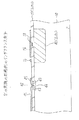
図4は、図3のインダクタンス素子の一部断面斜視図である。図4に示される通り、帯状導電膜16の下には、厚い絶縁領域40が形成される。更に、図4の帯状導電膜16の巻き線の内周部分には、複数のスリット34が形成される。帯状導電膜16に電流が流れることにより発生する磁束密度がより高い巻き線の内周部分に、複数のスリット34を設けることにより、帯状導電膜16内に発生する渦電流をより効率的に抑えることができる。
【0030】
図5は、更に別のインダクタンス素子の構造を示す平面図である。この例は、インダクタンス素子を構成する帯状導電膜内に発生する渦電流を抑える為に、その帯状導電膜を、巻き線方向の導電率がその垂直方向の導電率よりも大きい異方性の導電率をもつ材料により形成する。かかる材料は、例えば、セラミック系の酸化物超電導体である、Y2 Ba4 Cu7 O15やLaBa2 Cu3 O7 等である。或いは、別の材料として、ポリアセチレン等の有機導電材料である。これらの材料は、例えば、スパッタリング法や反応性蒸着法によりこれらの材料の薄膜を形成した後に、化学的エッチングやイオンエッチング法により任意の形状に加工するなどの方法により形成することで、一定方向の導電率がそれに垂直な方向の導電率よりも大きくなるようにすることができる。
【0031】
図5に示された例では、巻き線状の帯状導電膜を、図中の水平方向の下層配線161,163,165,167と、図中の垂直方向の上層配線160,162,164,166とで構成する。上記した方法により、先ず下層配線用の異方性導電材料層を形成し、図中の横方向のパターンにエッチングして、下層配線161,163,165,167を形成する。更に、その上に絶縁層を形成し上層と下層を接続するビア・ホールを形成し、さらに上層配線用の異方性導電材料層を形成し、図中の縦方向のパターンにエッチングして、上層配線160,162,164,166を形成する。その結果、一端16Aから他端16Bまでの巻き線状の帯状導電膜が形成される。
【0032】
下層配線161,163,165,167は、図中の矢印(図中水平方向)で示される巻き線方向の導電率が、それに垂直な方向の導電率よりも高い。また同様に、上層配線160,162,164,166は、図中の矢印(図中垂直方向)で示される巻き線方向の導電率が、それに垂直な方向の導電率よりも高い。従って、図5のインダクタンスの帯状導電膜は、その巻き線方向の導電性を犠牲にすることなく、それ自身に発生する渦電流を抑制することができる。
【0033】
【発明の効果】
以上説明した通り、本発明によれば、半導体基板上に形成されるインダクタンス素子において、インダクタンス素子を構成する帯状導電膜の下の基板表面に複数のPN接合を形成し、そのPN接合に逆バイアス電圧を印加して、基板表面が完全に空乏化するようにしたので、基板表面で発生する渦電流を抑えることができる。更に、基板表面の帯状導電膜による一次コイルと基板内部に発生する渦電流による二次コイルとの間の相互インダクタンスを低くすることができる。従って、インダクタンス素子の特性の損失を少なくすることができる。
【0034】
また、本発明によれば、半導体基板上に形成されるインダクタンス素子において、インダクタンスを構成する帯状導電膜の下の基板表面内部に分厚い絶縁領域を形成したので、基板内に発生する渦電流を抑えることができる。また、その厚い絶縁領域により、基板表面の帯状導電膜による一次コイルと基板内部に発生する渦電流による二次コイルとの間の相互インダクタンスを低くすることができる。従って、インダクタンス素子の特性の損失を少なくすることができる。
【0035】
また、本発明によれば、半導体基板上に形成されるインダクタンス素子において、インダクタンスを構成する帯状導電膜にスリットを形成したので、その帯状導電膜自体に発生する渦電流を抑えることができる。従って、インダクタンス素子の特性の損失を少なくすることができる。
【0036】
更に、本発明によれば、半導体基板上に形成されるインダクタンス素子において、インダクタンスを構成する帯状導電膜を、巻き線方向の導電率がそれと垂直方向の導電率より高い異方性導電率を有する材料で構成されるので、帯状導電膜自体に発生する渦電流を抑えることができる。従って、インダクタンス素子の特性の損失を少なくすることができる。
【図面の簡単な説明】
【図1】実施の形態例のインダクタンス素子の構造図である。
【図2】図1のインダクタンス素子に逆バイアス電圧を印加した時の詳細断面図である。
【図3】別の実施の形態例のインダクタンス素子の断面図である。
【図4】図3のインダクタンス素子の一部断面斜視図である。
【図5】別のインダクタンス素子の構造を示す平面図である。
【図6】公知例のインダクタンス素子の構造を示す図である。
【図7】図6の等価回路図である。
【符号の説明】
10 P型の半導体基板
12 配線用の絶縁膜
14 N型の不純物領域
16 巻き線状の帯状導電膜
20 渦電流
30 N型の埋込不純物領域
32 N型の不純物領域
34 スリット
40 厚い絶縁領域
160〜167 異方性導電率をもつ配線膜[0001]
BACKGROUND OF THE INVENTION
The present invention relates to an inductance element formed on a semiconductor substrate that constitutes an integrated circuit, and more particularly to an inductance element having a structure with low loss and low inductance reduction.
[0002]
[Prior art]
In recent years, downsizing of mobile communication devices such as mobile phones has been promoted. There is an increasing demand for configuring a high-frequency circuit used in such a small portable communication device with an integrated circuit using a silicon semiconductor. A high-frequency circuit requires an inductance element such as a coil or a transformer in addition to a transistor, a resistor, and a capacitor. Therefore, it is necessary to form an inductance element on the silicon semiconductor substrate together with an integrated circuit using transistors, resistors, and the like.
[0003]
Such an inductance element is generally realized by forming a strip-like conductive film such as aluminum in a spiral shape or a winding shape on an insulating film formed on the surface of a semiconductor substrate. However, in such a configuration, there is a semiconductor substrate in the immediate vicinity of the inductance element, and an eddy current that prevents a change in magnetic flux generated when a current is passed through the inductance element is generated in the semiconductor substrate, resulting in loss of characteristics. Are known.
[0004]
That is, when the band-shaped conductive layer formed in a winding shape is considered as a primary coil in a transformer, the semiconductor substrate containing impurities itself has a low resistance value, and thus acts like a short-circuited secondary coil in a high-frequency region. The loss due to the presence of the secondary coil is particularly noticeable in the high frequency region, and proposals have been made to prevent the generation of such eddy currents in the semiconductor substrate. For example, Japanese Patent Application Laid-Open No. 7-183468 shows that a plurality of PN junctions are formed on the surface of a silicon semiconductor substrate, and eddy currents are suppressed by a depletion layer generated at the junctions. That is, the eddy current path on the substrate surface is divided by a plurality of depletion layers to suppress the eddy current. Alternatively, Japanese Patent Application Laid-Open No. 7-235640 discloses a depletion layer formed at a junction of a plurality of PN junctions formed on the surface of a silicon semiconductor substrate and further applying a controlled reverse bias voltage to the PN junctions. It has been proposed to form an LC composite circuit element using the capacitance of This known example also shows that the generation of eddy currents can be suppressed by the depletion layer formed on the substrate surface.
[0005]
FIG. 6 is a diagram showing the structure of such a known inductance element. An N-
[0006]
In the configuration shown in FIG. 6, since a depletion layer is formed in a plurality of PN junctions, a large number of depletion layers are formed on the surface side of the
[0007]
[Problems to be solved by the invention]
However, in the above conventional example, only a plurality of depletion layers are formed on the surface of the
[0008]
Furthermore, as shown in the equivalent circuit diagram of FIG. 7, the impurity concentration of the
[0009]
As described above, the inductance element by the strip-like
[0010]
Further, as shown in FIG. 5, by passing a current 22 through the strip-shaped
[0011]
SUMMARY OF THE INVENTION Accordingly, an object of the present invention is to provide an inductance element having a structure in which insulation between a band-shaped conductive film formed on the surface of a semiconductor substrate and a region in the semiconductor substrate is further increased.
[0012]
Another object of the present invention is to provide an inductance element having a structure in which eddy currents generated in a strip-like conductive film itself formed on the surface of a semiconductor substrate are suppressed.
[0013]
[Means for Solving the Problems]
In order to achieve the above object, according to the first aspect of the present invention, a plurality of PN junctions are formed on the surface of a semiconductor substrate under a winding band-like conductive film constituting an inductance element, and a reverse bias is applied to the PN junctions. A voltage is applied to completely deplete the substrate surface. By applying a reverse bias to the PN junction, even if the impurity concentration on the surface of the substrate is high and adjacent PN junctions are separated to some extent, the extension of the depletion layer can be increased, and it can be completely depleted. become.
[0014]
Furthermore, in order to achieve the above object, the second invention provides a thick insulating region formed by an oxygen ion implantation method on the surface of the semiconductor substrate under the wound strip-shaped conductive film constituting the inductance element. Form. This insulating region has a larger film thickness than a thin insulating film for wiring formed on a normal integrated circuit element region. Due to the presence of the thick insulating region, the effective mutual inductance between the primary coil of the inductance element and the secondary coil due to the eddy current in the semiconductor substrate can be reduced. In addition, since more reliable insulation can be obtained than in the case of complete depletion using a plurality of PN junctions, the loss of the inductance element is small.
[0015]
Furthermore, in order to achieve the above object, in the third invention, a slit extending in the winding direction is formed in the strip-shaped conductive film formed in a winding shape, and a plurality of strips extending in the winding direction are formed in the strip-shaped conductive film. Use parallel wiring. By adopting such a configuration, it is possible to eliminate the path of eddy current generated in the strip-shaped conductive film, suppress eddy current, and suppress characteristic loss.
[0016]
Furthermore, in order to achieve the above object, according to the fourth aspect of the present invention, a strip-shaped conductive film formed in a winding shape is anisotropic in which the conductivity in the winding direction is higher than the conductivity in the direction perpendicular to the winding direction. It is made of a material having conductive conductivity. For example, by using an oxide superconductor or an organic conductive material, it is possible to form a strip-shaped conductive film having high conductivity in the winding direction and low conductivity in the direction perpendicular to the winding direction. In the case of such a material, an eddy current generated inside can be suppressed while preventing an increase in resistance in the winding direction of the belt-like conductive film.
[0017]
DETAILED DESCRIPTION OF THE INVENTION
Hereinafter, embodiments of the present invention will be described with reference to the drawings. However, the technical scope of the present invention is not limited to the embodiment.
[0018]
FIG. 1 is a structural diagram of an inductance element according to an embodiment. In this example, a plurality of N-
[0019]
A reverse bias voltage V is applied to the PN junction between the
[0020]
FIG. 2 is a detailed cross-sectional view when a reverse bias voltage is applied to the inductance element of FIG. Like the impurity concentration distribution shown on the right side of the figure, the
[0021]
The reverse bias voltage V applied between the PN junctions in the surface region of the
[0022]
In the example of FIG. 1, a plurality of N-
[0023]
In the present embodiment, the wound belt-like
[0024]
By forming the
[0025]
It is effective to form the
[0026]
FIG. 3 is a cross-sectional view of an inductance element according to another embodiment. FIG. 3 shows a strip-like
[0027]
On the other hand, a thick
[0028]
In this way, by forming the thick
[0029]
4 is a partial cross-sectional perspective view of the inductance element of FIG. As shown in FIG. 4, a thick
[0030]
FIG. 5 is a plan view showing the structure of still another inductance element. In this example, in order to suppress the eddy current generated in the strip-shaped conductive film constituting the inductance element, the strip-shaped conductive film is made to have an anisotropic conductivity in which the conductivity in the winding direction is larger than the conductivity in the vertical direction. It is made of a material with a rate. Such a material is, for example, Y 2 Ba 4 Cu 7 O 15 or LaBa 2 Cu 3 O 7 which is a ceramic oxide superconductor. Alternatively, another material is an organic conductive material such as polyacetylene. These materials are formed in a certain direction by, for example, forming a thin film of these materials by a sputtering method or a reactive vapor deposition method and then processing them into an arbitrary shape by a chemical etching or an ion etching method. Can be made larger than the conductivity in the direction perpendicular thereto.
[0031]
In the example shown in FIG. 5, the wound belt-like conductive film is made up of the
[0032]
The
[0033]
【The invention's effect】
As described above, according to the present invention, in the inductance element formed on the semiconductor substrate, a plurality of PN junctions are formed on the substrate surface under the strip-like conductive film constituting the inductance element, and the reverse bias is applied to the PN junction. Since a voltage is applied so that the substrate surface is completely depleted, eddy currents generated on the substrate surface can be suppressed. Furthermore, it is possible to reduce the mutual inductance between the primary coil due to the strip-like conductive film on the substrate surface and the secondary coil due to the eddy current generated inside the substrate. Therefore, the loss of the characteristic of the inductance element can be reduced.
[0034]
According to the present invention, in the inductance element formed on the semiconductor substrate, a thick insulating region is formed inside the substrate surface under the strip-shaped conductive film constituting the inductance, so that eddy currents generated in the substrate are suppressed. be able to. In addition, due to the thick insulating region, the mutual inductance between the primary coil due to the strip-like conductive film on the substrate surface and the secondary coil due to the eddy current generated inside the substrate can be reduced. Therefore, the loss of the characteristic of the inductance element can be reduced.
[0035]
According to the present invention, in the inductance element formed on the semiconductor substrate, since the slit is formed in the strip-shaped conductive film constituting the inductance, the eddy current generated in the strip-shaped conductive film itself can be suppressed. Therefore, the loss of the characteristic of the inductance element can be reduced.
[0036]
Furthermore, according to the present invention, in the inductance element formed on the semiconductor substrate, the strip-shaped conductive film constituting the inductance has an anisotropic conductivity in which the conductivity in the winding direction is higher than the conductivity in the direction perpendicular thereto. Since it is made of a material, eddy currents generated in the strip-shaped conductive film itself can be suppressed. Therefore, the loss of the characteristic of the inductance element can be reduced.
[Brief description of the drawings]
FIG. 1 is a structural diagram of an inductance element according to an embodiment.
2 is a detailed cross-sectional view when a reverse bias voltage is applied to the inductance element of FIG. 1;
FIG. 3 is a cross-sectional view of an inductance element according to another embodiment.
4 is a partial cross-sectional perspective view of the inductance element of FIG. 3;
FIG. 5 is a plan view showing the structure of another inductance element.
FIG. 6 is a diagram showing the structure of a known example of an inductance element.
7 is an equivalent circuit diagram of FIG. 6. FIG.
[Explanation of symbols]
10 P-
Claims (2)
前記半導体基板の表面に形成された複数のPN接合と、
前記複数のPN接合が形成された領域上の絶縁膜上に形成され、前記インダクタンス素子を構成する巻き線状の帯状導電膜と、
前記複数のPN接合間に逆バイアス電圧が印加されて、少なくとも前記半導体基板表面領域が完全に空乏化しているインダクタンス素子において、
前記半導体基板が一導電型であり、該基板の表面側から基板内部に向かって不純物濃度が増加する反対導電型の第1の不純物領域が前記基板の表面に形成されて前記PN接合が形成され、前記第1の不純物領域への逆バイアス電圧の印加は、当該第1の不純物領域の基板内部側から行われることを特徴とするインダクタンス素子。 An inductance element formed on a semiconductor substrate,
A plurality of PN junctions formed on the surface of the semiconductor substrate;
A wound belt-like conductive film formed on an insulating film on a region where the plurality of PN junctions are formed and constituting the inductance element;
In an inductance element in which a reverse bias voltage is applied between the plurality of PN junctions, and at least the semiconductor substrate surface region is completely depleted,
Before SL is a semiconductor substrate is one conductivity type, the PN junction first impurity region of opposite conductivity type impurity concentration increases from the surface side of the substrate in the substrate is formed on a surface of the substrate is formed The inductance element is characterized in that the reverse bias voltage is applied to the first impurity region from the inside of the substrate of the first impurity region.
Priority Applications (7)
| Application Number | Priority Date | Filing Date | Title |
|---|---|---|---|
| JP05962098A JP3942264B2 (en) | 1998-03-11 | 1998-03-11 | Inductance element formed on a semiconductor substrate |
| US09/175,975 US6225677B1 (en) | 1998-03-11 | 1998-10-21 | Inductance device formed on semiconductor substrate |
| TW087117512A TW401639B (en) | 1998-03-11 | 1998-10-22 | Inductance: device formed on semiconductor substrate |
| KR1019980044696A KR100334041B1 (en) | 1998-03-11 | 1998-10-24 | Inductance element formed on semiconductor substrate |
| FR9814825A FR2776128B1 (en) | 1998-03-11 | 1998-11-25 | INDUCTANCE DEVICE FORMED ON A SEMICONDUCTOR SUBSTRATE |
| US09/791,859 US20010040270A1 (en) | 1998-03-11 | 2001-02-26 | Inductance device formed on semiconductor substrate |
| US10/163,367 US6879022B2 (en) | 1998-03-11 | 2002-06-07 | Inductance device formed on semiconductor substrate |
Applications Claiming Priority (1)
| Application Number | Priority Date | Filing Date | Title |
|---|---|---|---|
| JP05962098A JP3942264B2 (en) | 1998-03-11 | 1998-03-11 | Inductance element formed on a semiconductor substrate |
Related Child Applications (2)
| Application Number | Title | Priority Date | Filing Date |
|---|---|---|---|
| JP2005068567A Division JP4230468B2 (en) | 2005-03-11 | 2005-03-11 | Inductance element formed on a semiconductor substrate |
| JP2006276864A Division JP2007005835A (en) | 2006-10-10 | 2006-10-10 | Inductance element formed on semiconductor substrate |
Publications (2)
| Publication Number | Publication Date |
|---|---|
| JPH11261008A JPH11261008A (en) | 1999-09-24 |
| JP3942264B2 true JP3942264B2 (en) | 2007-07-11 |
Family
ID=13118479
Family Applications (1)
| Application Number | Title | Priority Date | Filing Date |
|---|---|---|---|
| JP05962098A Expired - Fee Related JP3942264B2 (en) | 1998-03-11 | 1998-03-11 | Inductance element formed on a semiconductor substrate |
Country Status (5)
| Country | Link |
|---|---|
| US (3) | US6225677B1 (en) |
| JP (1) | JP3942264B2 (en) |
| KR (1) | KR100334041B1 (en) |
| FR (1) | FR2776128B1 (en) |
| TW (1) | TW401639B (en) |
Families Citing this family (44)
| Publication number | Priority date | Publication date | Assignee | Title |
|---|---|---|---|---|
| GB2353139B (en) * | 1999-08-12 | 2001-08-29 | United Microelectronics Corp | Inductor and method of manufacturing the same |
| JP4776752B2 (en) | 2000-04-19 | 2011-09-21 | ルネサスエレクトロニクス株式会社 | Semiconductor device |
| US6917095B1 (en) | 2000-05-30 | 2005-07-12 | Altera Corporation | Integrated radio frequency circuits |
| US6441442B1 (en) | 2000-05-30 | 2002-08-27 | Programmable Silicon Solutions | Integrated inductive circuits |
| US6455915B1 (en) * | 2000-05-30 | 2002-09-24 | Programmable Silicon Solutions | Integrated inductive circuits |
| EP1160842A3 (en) * | 2000-05-30 | 2003-09-17 | Programmable Silicon Solutions | Integrated radio frequency circuits |
| WO2001093317A1 (en) * | 2000-05-30 | 2001-12-06 | Programmable Silicon Solutions | Integrated inductive circuits |
| US6489663B2 (en) * | 2001-01-02 | 2002-12-03 | International Business Machines Corporation | Spiral inductor semiconducting device with grounding strips and conducting vias |
| DE10136740A1 (en) * | 2001-07-27 | 2002-10-24 | Infineon Technologies Ag | Integrated inductive component has region of second conductivity type inserted into semiconducting body, likewise lightly doped, arranged below region occupied by conducting track |
| JP3754406B2 (en) * | 2002-09-13 | 2006-03-15 | 富士通株式会社 | Variable inductor and method for adjusting inductance thereof |
| FR2846792A1 (en) * | 2002-10-30 | 2004-05-07 | Commissariat Energie Atomique | Radio-frequency microelectronic component and manufacturing method, comprises an inductive element placed on an insulator zone traversing the substrate and an insulated feedthrough |
| US20040195650A1 (en) * | 2003-04-04 | 2004-10-07 | Tsung-Ju Yang | High-Q inductor device with a shielding pattern embedded in a substrate |
| US6989578B2 (en) * | 2003-07-31 | 2006-01-24 | Taiwan Semiconductor Manufacturing Company | Inductor Q value improvement |
| WO2005024949A1 (en) * | 2003-08-28 | 2005-03-17 | Hitachi, Ltd. | Semiconductor device and its manufacturing method |
| DE102004014752B4 (en) * | 2004-03-25 | 2008-11-20 | Infineon Technologies Ag | Semiconductor device with coreless converter and half-bridge |
| US7250826B2 (en) * | 2005-07-19 | 2007-07-31 | Lctank Llc | Mutual inductance in transformer based tank circuitry |
| US7511588B2 (en) * | 2005-07-19 | 2009-03-31 | Lctank Llc | Flux linked LC tank circuits forming distributed clock networks |
| US7508280B2 (en) * | 2005-07-19 | 2009-03-24 | Lc Tank Llc | Frequency adjustment techniques in coupled LC tank circuits |
| US7786836B2 (en) * | 2005-07-19 | 2010-08-31 | Lctank Llc | Fabrication of inductors in transformer based tank circuitry |
| US7279426B2 (en) * | 2005-09-22 | 2007-10-09 | International Business Machines Corporation | Like integrated circuit devices with different depth |
| JP4647484B2 (en) * | 2005-12-27 | 2011-03-09 | ルネサスエレクトロニクス株式会社 | Semiconductor device |
| US7402890B2 (en) * | 2006-06-02 | 2008-07-22 | International Business Machines Corporation | Method for symmetric capacitor formation |
| GB2440365A (en) * | 2006-07-21 | 2008-01-30 | X Fab Uk Ltd | A semiconductor device |
| US7948055B2 (en) * | 2006-08-31 | 2011-05-24 | United Microelectronics Corp. | Inductor formed on semiconductor substrate |
| KR100883036B1 (en) * | 2007-07-25 | 2009-02-09 | 주식회사 동부하이텍 | Inductor for semiconductor device and method for fabricating the same |
| US20100193904A1 (en) * | 2009-01-30 | 2010-08-05 | Watt Jeffrey T | Integrated circuit inductor with doped substrate |
| GB0918221D0 (en) * | 2009-10-16 | 2009-12-02 | Cambridge Silicon Radio Ltd | Inductor structure |
| KR101121645B1 (en) * | 2010-03-22 | 2012-02-28 | 삼성전기주식회사 | Planar transformer |
| TWI498928B (en) * | 2010-08-04 | 2015-09-01 | Richwave Technology Corp | Spiral inductor device |
| CN102376700A (en) * | 2010-08-04 | 2012-03-14 | 立积电子股份有限公司 | Electronic component, manufacturing method of electronic component, spiral inductance component and manufacturing method of spiral inductance component |
| US8686539B1 (en) * | 2010-10-15 | 2014-04-01 | Xilinx, Inc. | Inductor having a deep-well noise isolation shield |
| WO2012121724A1 (en) * | 2011-03-09 | 2012-09-13 | Hewlett-Packard Development Company, L.P. | Flat power coil for wireless charging applications |
| CN102522385A (en) * | 2011-12-30 | 2012-06-27 | 上海集成电路研发中心有限公司 | On-sheet integrated copper inductor |
| US8878334B1 (en) * | 2012-03-23 | 2014-11-04 | Altera Corporation | Integrated circuit resistors with reduced parasitic capacitance |
| JP6057534B2 (en) * | 2012-04-18 | 2017-01-11 | 住重試験検査株式会社 | Manufacturing method of semiconductor device |
| CN103474414B (en) * | 2012-06-06 | 2016-03-16 | 中芯国际集成电路制造(上海)有限公司 | Inductance and forming method thereof |
| JP5719000B2 (en) * | 2013-09-17 | 2015-05-13 | 学校法人慶應義塾 | Integrated circuit device |
| JP6375872B2 (en) * | 2014-10-29 | 2018-08-22 | 住友電気工業株式会社 | Superconducting magnet and superconducting equipment |
| TWI587329B (en) * | 2014-10-31 | 2017-06-11 | 台灣東電化股份有限公司 | A wireless charging coil pcb structure |
| JP7056016B2 (en) * | 2017-06-13 | 2022-04-19 | Tdk株式会社 | Coil parts |
| JP7169871B2 (en) * | 2018-12-26 | 2022-11-11 | 住重アテックス株式会社 | Semiconductor device manufacturing method |
| JP7430376B2 (en) * | 2019-12-19 | 2024-02-13 | 三安ジャパンテクノロジー株式会社 | Spiral inductors and passive integrated circuits |
| KR20220102772A (en) | 2021-01-14 | 2022-07-21 | 주식회사 삼주유니콘 | Apparatus for adjusting length of round tube |
| CN113745404A (en) * | 2021-08-25 | 2021-12-03 | 中国科学院微电子研究所 | Spiral inductor preparation method, spiral inductor and passive device module |
Family Cites Families (17)
| Publication number | Priority date | Publication date | Assignee | Title |
|---|---|---|---|---|
| US4851257A (en) | 1987-03-13 | 1989-07-25 | Harris Corporation | Process for the fabrication of a vertical contact |
| US5070317A (en) * | 1989-01-17 | 1991-12-03 | Bhagat Jayant K | Miniature inductor for integrated circuits and devices |
| US5206213A (en) * | 1990-03-23 | 1993-04-27 | International Business Machines Corp. | Method of preparing oriented, polycrystalline superconducting ceramic oxides |
| EP0560396B1 (en) * | 1992-03-13 | 2001-11-07 | Kabushiki Kaisha Toshiba | Nuclear magnetic resonance imaging with improved image quality and operation efficiency |
| US5572040A (en) * | 1993-07-12 | 1996-11-05 | Peregrine Semiconductor Corporation | High-frequency wireless communication system on a single ultrathin silicon on sapphire chip |
| US5370766A (en) | 1993-08-16 | 1994-12-06 | California Micro Devices | Methods for fabrication of thin film inductors, inductor networks and integration with other passive and active devices |
| JP3015679B2 (en) | 1993-09-01 | 2000-03-06 | 株式会社東芝 | Semiconductor device and manufacturing method thereof |
| JP3373267B2 (en) | 1993-11-01 | 2003-02-04 | 新潟精密株式会社 | LC element and semiconductor device |
| JPH07183468A (en) | 1993-12-22 | 1995-07-21 | Tokin Corp | Insulating silicon substrate and inductor using the substrate, and distribution constant type filter |
| TW267260B (en) * | 1993-12-29 | 1996-01-01 | Tif Kk | |
| JP3450408B2 (en) | 1994-02-21 | 2003-09-22 | 新潟精密株式会社 | LC composite element |
| KR970053797A (en) * | 1995-12-21 | 1997-07-31 | 양승택 | Inductor Using Depletion Layer |
| JP2904086B2 (en) * | 1995-12-27 | 1999-06-14 | 日本電気株式会社 | Semiconductor device and manufacturing method thereof |
| SE510443C2 (en) * | 1996-05-31 | 1999-05-25 | Ericsson Telefon Ab L M | Inductors for integrated circuits |
| KR100314610B1 (en) * | 1996-08-09 | 2001-12-28 | 윤덕용 | Supper high frequency device using oxidized porous silicon substrate |
| KR100243658B1 (en) * | 1996-12-06 | 2000-02-01 | 정선종 | Inductor device using substrate biasing technigue and method for fabricating the same |
| US5844299A (en) | 1997-01-31 | 1998-12-01 | National Semiconductor Corporation | Integrated inductor |
-
1998
- 1998-03-11 JP JP05962098A patent/JP3942264B2/en not_active Expired - Fee Related
- 1998-10-21 US US09/175,975 patent/US6225677B1/en not_active Expired - Lifetime
- 1998-10-22 TW TW087117512A patent/TW401639B/en not_active IP Right Cessation
- 1998-10-24 KR KR1019980044696A patent/KR100334041B1/en not_active IP Right Cessation
- 1998-11-25 FR FR9814825A patent/FR2776128B1/en not_active Expired - Fee Related
-
2001
- 2001-02-26 US US09/791,859 patent/US20010040270A1/en not_active Abandoned
-
2002
- 2002-06-07 US US10/163,367 patent/US6879022B2/en not_active Expired - Fee Related
Also Published As
| Publication number | Publication date |
|---|---|
| US20010040270A1 (en) | 2001-11-15 |
| FR2776128A1 (en) | 1999-09-17 |
| US20020149088A1 (en) | 2002-10-17 |
| KR19990076525A (en) | 1999-10-15 |
| KR100334041B1 (en) | 2002-09-25 |
| US6225677B1 (en) | 2001-05-01 |
| FR2776128B1 (en) | 2005-04-15 |
| TW401639B (en) | 2000-08-11 |
| JPH11261008A (en) | 1999-09-24 |
| US6879022B2 (en) | 2005-04-12 |
Similar Documents
| Publication | Publication Date | Title |
|---|---|---|
| JP3942264B2 (en) | Inductance element formed on a semiconductor substrate | |
| US5952704A (en) | Inductor devices using substrate biasing technique | |
| US20020158306A1 (en) | Semiconductor device with a spiral inductor | |
| US20090206376A1 (en) | Semiconductor device | |
| TWI411227B (en) | Integrated filter structure having improved interchannel isolation | |
| JPH10242470A (en) | Semiconductor device and fabrication thereof | |
| JP2011029503A (en) | Semiconductor device | |
| JP2002110908A (en) | Spiral inductor and method for manufacturing semiconductor integrated circuit device having the same | |
| US6008713A (en) | Monolithic inductor | |
| US5929490A (en) | Semiconductor device with an improved body contact hole structure | |
| US5225356A (en) | Method of making field-effect semiconductor device on sot | |
| US10381457B2 (en) | Transistor with contacted deep well region | |
| WO2014050422A1 (en) | Chip diode and method for manufacturing same | |
| JP4230468B2 (en) | Inductance element formed on a semiconductor substrate | |
| US6849913B2 (en) | Integrated circuit including an inductor, active layers with isolation dielectrics, and multiple insulation layers | |
| US20030077845A1 (en) | Integrated circuit and manufacturing method therefor | |
| JP2004031922A (en) | Semiconductor device | |
| JPH09270515A (en) | Semiconductor device | |
| JP2007005835A (en) | Inductance element formed on semiconductor substrate | |
| JP3932443B2 (en) | Semiconductor element | |
| US20240297071A1 (en) | Semiconductor device and method of manufacturing semiconductor device | |
| JP2001298195A (en) | Mos transistor | |
| JPH05110075A (en) | Insulated gate type field effect transistor | |
| JP2009252965A (en) | Semiconductor device | |
| JPS62224079A (en) | Field-effect transistor |
Legal Events
| Date | Code | Title | Description |
|---|---|---|---|
| A521 | Written amendment |
Free format text: JAPANESE INTERMEDIATE CODE: A523 Effective date: 20050309 |
|
| A621 | Written request for application examination |
Free format text: JAPANESE INTERMEDIATE CODE: A621 Effective date: 20050309 |
|
| A977 | Report on retrieval |
Free format text: JAPANESE INTERMEDIATE CODE: A971007 Effective date: 20060728 |
|
| A131 | Notification of reasons for refusal |
Free format text: JAPANESE INTERMEDIATE CODE: A131 Effective date: 20060808 |
|
| A521 | Written amendment |
Free format text: JAPANESE INTERMEDIATE CODE: A523 Effective date: 20061010 |
|
| TRDD | Decision of grant or rejection written | ||
| A01 | Written decision to grant a patent or to grant a registration (utility model) |
Free format text: JAPANESE INTERMEDIATE CODE: A01 Effective date: 20070403 |
|
| A61 | First payment of annual fees (during grant procedure) |
Free format text: JAPANESE INTERMEDIATE CODE: A61 Effective date: 20070403 |
|
| R150 | Certificate of patent or registration of utility model |
Free format text: JAPANESE INTERMEDIATE CODE: R150 |
|
| S111 | Request for change of ownership or part of ownership |
Free format text: JAPANESE INTERMEDIATE CODE: R313111 |
|
| FPAY | Renewal fee payment (event date is renewal date of database) |
Free format text: PAYMENT UNTIL: 20100413 Year of fee payment: 3 |
|
| R350 | Written notification of registration of transfer |
Free format text: JAPANESE INTERMEDIATE CODE: R350 |
|
| FPAY | Renewal fee payment (event date is renewal date of database) |
Free format text: PAYMENT UNTIL: 20110413 Year of fee payment: 4 |
|
| FPAY | Renewal fee payment (event date is renewal date of database) |
Free format text: PAYMENT UNTIL: 20110413 Year of fee payment: 4 |
|
| S531 | Written request for registration of change of domicile |
Free format text: JAPANESE INTERMEDIATE CODE: R313531 |
|
| S533 | Written request for registration of change of name |
Free format text: JAPANESE INTERMEDIATE CODE: R313533 |
|
| FPAY | Renewal fee payment (event date is renewal date of database) |
Free format text: PAYMENT UNTIL: 20110413 Year of fee payment: 4 |
|
| R350 | Written notification of registration of transfer |
Free format text: JAPANESE INTERMEDIATE CODE: R350 |
|
| FPAY | Renewal fee payment (event date is renewal date of database) |
Free format text: PAYMENT UNTIL: 20120413 Year of fee payment: 5 |
|
| FPAY | Renewal fee payment (event date is renewal date of database) |
Free format text: PAYMENT UNTIL: 20130413 Year of fee payment: 6 |
|
| FPAY | Renewal fee payment (event date is renewal date of database) |
Free format text: PAYMENT UNTIL: 20130413 Year of fee payment: 6 |
|
| FPAY | Renewal fee payment (event date is renewal date of database) |
Free format text: PAYMENT UNTIL: 20140413 Year of fee payment: 7 |
|
| S111 | Request for change of ownership or part of ownership |
Free format text: JAPANESE INTERMEDIATE CODE: R313111 |
|
| R350 | Written notification of registration of transfer |
Free format text: JAPANESE INTERMEDIATE CODE: R350 |
|
| LAPS | Cancellation because of no payment of annual fees |