JP4753826B2 - 多出力電源装置 - Google Patents
多出力電源装置 Download PDFInfo
- Publication number
- JP4753826B2 JP4753826B2 JP2006264025A JP2006264025A JP4753826B2 JP 4753826 B2 JP4753826 B2 JP 4753826B2 JP 2006264025 A JP2006264025 A JP 2006264025A JP 2006264025 A JP2006264025 A JP 2006264025A JP 4753826 B2 JP4753826 B2 JP 4753826B2
- Authority
- JP
- Japan
- Prior art keywords
- power supply
- circuit
- voltage
- output
- switch element
- Prior art date
- Legal status (The legal status is an assumption and is not a legal conclusion. Google has not performed a legal analysis and makes no representation as to the accuracy of the status listed.)
- Expired - Fee Related
Links
- 239000003990 capacitor Substances 0.000 description 18
- 238000010586 diagram Methods 0.000 description 9
- 230000007423 decrease Effects 0.000 description 3
- 238000009499 grossing Methods 0.000 description 2
- 238000000034 method Methods 0.000 description 1
Images


Classifications
-
- H—ELECTRICITY
- H02—GENERATION; CONVERSION OR DISTRIBUTION OF ELECTRIC POWER
- H02J—CIRCUIT ARRANGEMENTS OR SYSTEMS FOR SUPPLYING OR DISTRIBUTING ELECTRIC POWER; SYSTEMS FOR STORING ELECTRIC ENERGY
- H02J1/00—Circuit arrangements for dc mains or dc distribution networks
- H02J1/08—Three-wire systems; Systems having more than three wires
-
- H—ELECTRICITY
- H02—GENERATION; CONVERSION OR DISTRIBUTION OF ELECTRIC POWER
- H02J—CIRCUIT ARRANGEMENTS OR SYSTEMS FOR SUPPLYING OR DISTRIBUTING ELECTRIC POWER; SYSTEMS FOR STORING ELECTRIC ENERGY
- H02J1/00—Circuit arrangements for dc mains or dc distribution networks
- H02J1/10—Parallel operation of dc sources
- H02J1/108—Parallel operation of dc sources using diodes blocking reverse current flow
-
- H—ELECTRICITY
- H02—GENERATION; CONVERSION OR DISTRIBUTION OF ELECTRIC POWER
- H02J—CIRCUIT ARRANGEMENTS OR SYSTEMS FOR SUPPLYING OR DISTRIBUTING ELECTRIC POWER; SYSTEMS FOR STORING ELECTRIC ENERGY
- H02J1/00—Circuit arrangements for dc mains or dc distribution networks
- H02J1/08—Three-wire systems; Systems having more than three wires
- H02J1/082—Plural DC voltage, e.g. DC supply voltage with at least two different DC voltage levels
Description

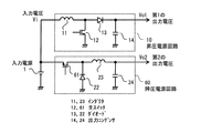
図1は本発明の実施形態1に係る多出力電源装置を示す回路構成図である。
ここで、前記従来例を示す図5において説明した構成部材に対応し同等の機能を有するものには同一の符号を付して示す。
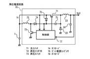
図4は本発明の実施形態2に係る多出力電源装置の回路構成図であり、前述の実施形態1における降圧電源回路20として構成した第2の電源回路を第3の電源回路(反転電源回路40)で構成したものである。図4に示すように、第3の電源回路の反転電源回路40は、入力電圧Viを反転昇降圧して第3の出力電圧Vo3を出力する。
10 昇圧電源回路
11,23,42 インダクタ
12,61,71 主スイッチ
13,22,43,74,76 ダイオード
14,24,44 出力コンデンサ
15 第1の制御回路
21 主スイッチ回路
25 第2の制御回路
26,46 第1のスイッチ素子
27,47 第2のスイッチ素子
28,48 第1の駆動回路
29,49 インバータ
30,50 第2の駆動回路
45 第3の制御回路
60,70 降圧電源回路
72 昇圧インダクタ
73 昇圧スイッチ
75 ゲート電源コンデンサ
77 制御部
Claims (5)
- 入力電源から供給の入力電圧を昇圧して第1の出力電圧を出力する第1の電源回路と、前記入力電源に接続した主スイッチ回路を介した前記入力電圧から第2の出力電圧を出力する第2の電源回路とを備え、
前記第2の電源回路の主スイッチ回路は、制御端子を低電位側に引かれることでオン状態となる第1のスイッチ素子と、制御端子を高電位側に引かれることでオン状態となる第2のスイッチ素子との並列構成を有し、前記第2のスイッチ素子の制御端子への印加電圧源を前記第1の電源回路の第1の出力電圧とすることを特徴とする多出力電源装置。 - 前記第2の電源回路は、前記入力電圧を降圧して前記第2の出力電圧を出力する降圧コンバータであることを特徴とする請求項1記載の多出力電源装置。
- 前記第2の電源回路は、前記入力電圧を反転して前記第2の出力電圧を出力する反転コンバータであることを特徴とする請求項1記載の多出力電源装置。
- 前記主スイッチ回路を並列構成する前記第1のスイッチ素子はPMOSトランジスタであり、前記第2のスイッチ素子はNMOSトランジスタであることを特徴とする請求項1〜3のいずれか1項に記載の多出力電源装置。
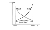
- 前記第1のスイッチ素子の最大入力電圧時におけるオン抵抗と、前記第2のスイッチ素子の最小入力電圧時におけるオン抵抗が、ほぼ等しくなるように前記第1,第2のスイッチ素子のトランジスタサイズを設定したことを特徴とする請求項4記載の多出力電源装置。
Priority Applications (2)
| Application Number | Priority Date | Filing Date | Title |
|---|---|---|---|
| JP2006264025A JP4753826B2 (ja) | 2006-09-28 | 2006-09-28 | 多出力電源装置 |
| US11/902,880 US7586212B2 (en) | 2006-09-28 | 2007-09-26 | Multi-output power supply apparatus |
Applications Claiming Priority (1)
| Application Number | Priority Date | Filing Date | Title |
|---|---|---|---|
| JP2006264025A JP4753826B2 (ja) | 2006-09-28 | 2006-09-28 | 多出力電源装置 |
Publications (2)
| Publication Number | Publication Date |
|---|---|
| JP2008086133A JP2008086133A (ja) | 2008-04-10 |
| JP4753826B2 true JP4753826B2 (ja) | 2011-08-24 |
Family
ID=39356410
Family Applications (1)
| Application Number | Title | Priority Date | Filing Date |
|---|---|---|---|
| JP2006264025A Expired - Fee Related JP4753826B2 (ja) | 2006-09-28 | 2006-09-28 | 多出力電源装置 |
Country Status (2)
| Country | Link |
|---|---|
| US (1) | US7586212B2 (ja) |
| JP (1) | JP4753826B2 (ja) |
Families Citing this family (4)
| Publication number | Priority date | Publication date | Assignee | Title |
|---|---|---|---|---|
| US8044536B2 (en) * | 2007-10-10 | 2011-10-25 | Ams Research Corporation | Powering devices having low and high voltage circuits |
| CN102005919B (zh) * | 2009-09-02 | 2014-03-12 | 瑞萨集成电路设计(北京)有限公司 | 一种升压型dc-dc转换器及方法 |
| ES2692372T3 (es) | 2010-11-22 | 2018-12-03 | Saab Ab | Disposición de suministro de energía para distribución de energía |
| JP6031883B2 (ja) * | 2012-08-08 | 2016-11-24 | 富士通株式会社 | 半導体集積回路及び電源回路 |
Family Cites Families (8)
| Publication number | Priority date | Publication date | Assignee | Title |
|---|---|---|---|---|
| JPS5834494Y2 (ja) * | 1977-06-18 | 1983-08-03 | ソニー株式会社 | 電源回路 |
| US4644251A (en) * | 1985-04-01 | 1987-02-17 | Motorola, Inc. | Dual voltage tracking control device |
| JP3000633B2 (ja) * | 1990-07-18 | 2000-01-17 | セイコーエプソン株式会社 | 電子機器 |
| JPH07222439A (ja) | 1994-02-02 | 1995-08-18 | Fuji Electric Co Ltd | Dc−dcコンバータ |
| JP2005117886A (ja) | 2003-09-19 | 2005-04-28 | Matsushita Electric Ind Co Ltd | 多出力dc−dcコンバータ |
| JP4201205B2 (ja) | 2004-06-15 | 2008-12-24 | パナソニック株式会社 | 多出力電源回路及びそれを用いた電子機器 |
| JP2006014910A (ja) | 2004-07-01 | 2006-01-19 | Akihiko Maeda | 洗濯ネット |
| JP4832240B2 (ja) * | 2006-09-29 | 2011-12-07 | パナソニック株式会社 | 多出力電源装置 |
-
2006
- 2006-09-28 JP JP2006264025A patent/JP4753826B2/ja not_active Expired - Fee Related
-
2007
- 2007-09-26 US US11/902,880 patent/US7586212B2/en active Active
Also Published As
| Publication number | Publication date |
|---|---|
| US7586212B2 (en) | 2009-09-08 |
| JP2008086133A (ja) | 2008-04-10 |
| US20080179950A1 (en) | 2008-07-31 |
Similar Documents
| Publication | Publication Date | Title |
|---|---|---|
| JP5297116B2 (ja) | 昇圧回路及びこれを用いた電源装置 | |
| JP4781744B2 (ja) | 電源装置及びこれを用いた電気機器 | |
| US20120091978A1 (en) | Dc-dc converter | |
| JP2010110070A (ja) | Dc−dcコンバータ | |
| US9667144B2 (en) | DC-DC converter with reverse current detecting circuit | |
| JP2008022642A (ja) | Dc−dcコンバータ | |
| JP2010004692A (ja) | フラッシュ用電源装置 | |
| JP5866920B2 (ja) | スイッチング装置及びその制御方法 | |
| JP5098760B2 (ja) | Dc−dcコンバータおよび電源制御用半導体集積回路 | |
| JP2012253953A (ja) | 昇圧型dc−dcコンバータ | |
| JP5157603B2 (ja) | 昇圧型dc−dcコンバータおよび電源駆動用半導体集積回路 | |
| JP2010004691A (ja) | フラッシュ用電源装置 | |
| JP2007244086A (ja) | スイッチング電源装置のソフトスタート回路 | |
| JP4753826B2 (ja) | 多出力電源装置 | |
| JP2009022092A (ja) | 多出力電源回路 | |
| JP2008060492A (ja) | 発光素子駆動装置 | |
| JP5951358B2 (ja) | 充電制御回路および充電回路 | |
| US8159089B2 (en) | Power supply circuit and semiconductor device for use therein | |
| JP2014011841A (ja) | スイッチングレギュレータ | |
| JP2007089333A (ja) | 昇降圧コンバータ | |
| US10333400B2 (en) | Boost DC-DC converter including a switching element | |
| JP2008166076A (ja) | 電子機器システム、および電源制御方法 | |
| JP6409171B2 (ja) | スイッチング電源装置、電子機器及び双方向dcdcコンバータ | |
| US20090058385A1 (en) | Step-up DC-DC converter | |
| WO2023153085A1 (ja) | 充放電装置及び充放電の制御方法 |
Legal Events
| Date | Code | Title | Description |
|---|---|---|---|
| A621 | Written request for application examination |
Free format text: JAPANESE INTERMEDIATE CODE: A621 Effective date: 20081203 |
|
| RD03 | Notification of appointment of power of attorney |
Free format text: JAPANESE INTERMEDIATE CODE: A7423 Effective date: 20100917 |
|
| RD04 | Notification of resignation of power of attorney |
Free format text: JAPANESE INTERMEDIATE CODE: A7424 Effective date: 20100927 |
|
| A977 | Report on retrieval |
Free format text: JAPANESE INTERMEDIATE CODE: A971007 Effective date: 20110420 |
|
| TRDD | Decision of grant or rejection written | ||
| A01 | Written decision to grant a patent or to grant a registration (utility model) |
Free format text: JAPANESE INTERMEDIATE CODE: A01 Effective date: 20110426 |
|
| A61 | First payment of annual fees (during grant procedure) |
Free format text: JAPANESE INTERMEDIATE CODE: A61 Effective date: 20110524 |
|
| FPAY | Renewal fee payment (event date is renewal date of database) |
Free format text: PAYMENT UNTIL: 20140603 Year of fee payment: 3 |
|
| R151 | Written notification of patent or utility model registration |
Ref document number: 4753826 Country of ref document: JP Free format text: JAPANESE INTERMEDIATE CODE: R151 |
|
| FPAY | Renewal fee payment (event date is renewal date of database) |
Free format text: PAYMENT UNTIL: 20140603 Year of fee payment: 3 |
|
| S111 | Request for change of ownership or part of ownership |
Free format text: JAPANESE INTERMEDIATE CODE: R313113 |
|
| R350 | Written notification of registration of transfer |
Free format text: JAPANESE INTERMEDIATE CODE: R350 |
|
| R250 | Receipt of annual fees |
Free format text: JAPANESE INTERMEDIATE CODE: R250 |
|
| R250 | Receipt of annual fees |
Free format text: JAPANESE INTERMEDIATE CODE: R250 |
|
| LAPS | Cancellation because of no payment of annual fees |