JP4753826B2 - Multi-output power supply - Google Patents
Multi-output power supply Download PDFInfo
- Publication number
- JP4753826B2 JP4753826B2 JP2006264025A JP2006264025A JP4753826B2 JP 4753826 B2 JP4753826 B2 JP 4753826B2 JP 2006264025 A JP2006264025 A JP 2006264025A JP 2006264025 A JP2006264025 A JP 2006264025A JP 4753826 B2 JP4753826 B2 JP 4753826B2
- Authority
- JP
- Japan
- Prior art keywords
- power supply
- circuit
- voltage
- output
- switch element
- Prior art date
- Legal status (The legal status is an assumption and is not a legal conclusion. Google has not performed a legal analysis and makes no representation as to the accuracy of the status listed.)
- Expired - Fee Related
Links
- 239000003990 capacitor Substances 0.000 description 18
- 238000010586 diagram Methods 0.000 description 9
- 230000007423 decrease Effects 0.000 description 3
- 238000009499 grossing Methods 0.000 description 2
- 238000000034 method Methods 0.000 description 1
Images


Classifications
-
- H—ELECTRICITY
- H02—GENERATION; CONVERSION OR DISTRIBUTION OF ELECTRIC POWER
- H02J—CIRCUIT ARRANGEMENTS OR SYSTEMS FOR SUPPLYING OR DISTRIBUTING ELECTRIC POWER; SYSTEMS FOR STORING ELECTRIC ENERGY
- H02J1/00—Circuit arrangements for dc mains or dc distribution networks
- H02J1/08—Three-wire systems; Systems having more than three wires
-
- H—ELECTRICITY
- H02—GENERATION; CONVERSION OR DISTRIBUTION OF ELECTRIC POWER
- H02J—CIRCUIT ARRANGEMENTS OR SYSTEMS FOR SUPPLYING OR DISTRIBUTING ELECTRIC POWER; SYSTEMS FOR STORING ELECTRIC ENERGY
- H02J1/00—Circuit arrangements for dc mains or dc distribution networks
- H02J1/10—Parallel operation of dc sources
- H02J1/108—Parallel operation of dc sources using diodes blocking reverse current flow
-
- H—ELECTRICITY
- H02—GENERATION; CONVERSION OR DISTRIBUTION OF ELECTRIC POWER
- H02J—CIRCUIT ARRANGEMENTS OR SYSTEMS FOR SUPPLYING OR DISTRIBUTING ELECTRIC POWER; SYSTEMS FOR STORING ELECTRIC ENERGY
- H02J1/00—Circuit arrangements for dc mains or dc distribution networks
- H02J1/08—Three-wire systems; Systems having more than three wires
- H02J1/082—Plural DC voltage, e.g. DC supply voltage with at least two different DC voltage levels
Description
本発明は、昇圧電源回路と、降圧電源回路または反転電源回路を含む多出力電源装置に関するものである。 The present invention relates to a multi-output power supply device including a step-up power supply circuit and a step-down power supply circuit or an inverting power supply circuit.
近年、携帯機器として用いられる電子機器はバッテリーを電力源とし、このバッテリー電圧を機器内における各種電子回路への所望の電源電圧に変換するため、複数の電源回路からなる多出力電源装置が搭載されている。このバッテリー電圧は機器の動作時間を稼ぐため、より低電圧まで使用される傾向があり、例えば単三乾電池2セルの場合、初期入力電圧3.4Vに対して下限入力電圧は1.5〜1.8Vといった入力仕様になる。一方、要望される電源電圧は多種多様であり、例えばデジタルスチルカメラの場合、レンズ駆動用の5VやDSP(Digital Signal Processor)用の1.2Vがある。電源装置において、5Vを生成するためには昇圧電源回路が、1.2Vを生成するためには降圧電源回路が必要になる。 In recent years, an electronic device used as a portable device uses a battery as a power source, and in order to convert the battery voltage into a desired power supply voltage to various electronic circuits in the device, a multi-output power supply device including a plurality of power supply circuits is mounted. ing. This battery voltage tends to be used up to a lower voltage in order to increase the operating time of the device. For example, in the case of 2 AA batteries, the lower limit input voltage is 1.5 to 1 with respect to the initial input voltage 3.4V. The input specification is .8V. On the other hand, various power supply voltages are required. For example, in the case of a digital still camera, there are 5V for driving a lens and 1.2V for a DSP (Digital Signal Processor). In the power supply device, a step-up power supply circuit is required to generate 5V, and a step-down power supply circuit is required to generate 1.2V.
図5に従来の昇圧電源回路と降圧電源回路からなる多出力電源装置の回路構成を示す。図5に示すように、昇圧電源回路10は、入力電圧Viを供給する入力電源1に接続されたインダクタ11、インダクタ11の他端に接続されたNMOSトランジスタからなる主スイッチ12、主スイッチ12の電圧を整流平滑するダイオード13と出力コンデンサ14から構成される。
FIG. 5 shows a circuit configuration of a conventional multi-output power supply device including a step-up power supply circuit and a step-down power supply circuit. As shown in FIG. 5, the boost
主スイッチ12のスイッチング動作によってインダクタ11へのエネルギーの蓄積と放出が繰り返され、主スイッチ12のオフ時においてインダクタ11からダイオード13を介して出力コンデンサ14を充電する電流が流れる。主スイッチ12の1スイッチング周期に占めるオン時間の割合をデューティ比δ1とし、ダイオード13の順方向電圧降下等を無視すると、昇圧電源回路10の第1の出力電圧Vo1は、(数1)
By the switching operation of the

図5において、降圧電源回路60は、入力電圧Viを供給する入力電源1に接続されたPMOSトランジスタからなる主スイッチ61、主スイッチ61の他端に接続されたダイオード22、主スイッチ61とダイオード22の接続点電圧を平滑するインダクタ23と出力コンデンサ24から構成される。
In FIG. 5, a step-down
主スイッチ61のスイッチング動作によってインダクタ23へのエネルギーの蓄積と放出が繰り返され、インダクタ23を介して出力コンデンサ24を充電する電流が流れる。主スイッチ61の1スイッチング周期に占めるオン時間の割合をデューティ比δ2とし、ダイオード22の順方向電圧降下等を無視すると、降圧電源回路60の第2の出力電圧Vo2は、(数2)
By the switching operation of the
![]()
![]()
一般にNMOSトランジスタに比べてPMOSトランジスタは、同じ形状であればオン電圧が高くなるなど特性が悪化する。このため入力電圧Viが上述のように1.5〜1.8Vと低くなると、降圧電源回路60では主スイッチ61のオン電圧が高くなり、出力供給不足が発生する。そこで、降圧電源回路60の主スイッチ61をNMOSトランジスタで構成する場合がある。
In general, compared with an NMOS transistor, a PMOS transistor has the same characteristics, such as a higher on-voltage, which deteriorates characteristics. For this reason, when the input voltage Vi is as low as 1.5 to 1.8 V as described above, the on-voltage of the
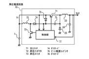
図6は、特許文献1に開示されている降圧電源回路の回路構成図である。図6に示すように、降圧電源回路70は、入力電圧Viを供給する入力電源1に接続されたNMOSトランジスタからなる主スイッチ71、ダイオード22、インダクタ23と出力コンデンサ24からなり、さらに入力電源1に並列に直列接続された昇圧インダクタ72とNMOSトランジスタからなる昇圧スイッチ73と、昇圧インダクタ72と昇圧スイッチ73の接続点電圧を整流するダイオード74と、ダイオード74のカソードとダイオード22のカソードの間に接続されたゲート電源コンデンサ75と、入力電源1からゲート電源コンデンサ75に接続されたダイオード76と、主スイッチ71と昇圧スイッチ73をオンオフする制御部77とから構成される。
FIG. 6 is a circuit configuration diagram of the step-down power supply circuit disclosed in
制御部77は、入力電圧Viが所定値より低い時、または主スイッチ71がデューティ比100%でオン状態にある時、昇圧スイッチ73をスイッチングする。このことにより、昇圧スイッチ73のオフ時に昇圧インダクタ72はダイオード74を介してゲート電源コンデンサ75を充電し、主スイッチ71をオンできるゲート用電源を得る。昇圧インダクタ72、昇圧スイッチ73とダイオード74は、ゲート用電源を得るための昇圧コンバータを構成している。
The
次に、入力電圧Viが所定値を上回り、かつ主スイッチ71がスイッチングしている時、制御部77は昇圧スイッチ73の駆動を停止する。このことにより、主スイッチ71がオフ時にダイオード76の導通によって、ゲート電源コンデンサ75はダイオード76を介して入力電圧Viにより充電され、主スイッチ71をオンできるゲート用電源を得る。このようなダイオード76とゲート電源コンデンサ75の構成をブートストラップ回路という。以上のように、主スイッチ71にNMOSトランジスタを用いた降圧電源回路70のゲート用電源電圧が、昇圧コンバータやブートストラップ回路により確保される。
前述したような、単に昇圧電源回路と降圧電源回路からなる従来の多出力電源装置では、降圧電源回路の主スイッチにPMOSトランジスタが用いられていると、入力電圧が低い場合、降圧電源回路では主スイッチのオン電圧が高くなり、出力供給不足が発生するという問題がある。これの対策として図6に示したように、降圧電源回路の主スイッチにNMOSトランジスタを用いて、NMOSトランジスタを駆動するためのゲート用電源を昇圧コンバータやブートストラップで生成する方法がある。しかしながら、ブートストラップ回路で生成されるゲート用電源は入力電圧であるため、降圧電源回路の主スイッチのゲートには入力電圧の2倍の電圧が印加されることになり、高入力時に耐圧を越える危険性があるという問題がある。 As described above, in the conventional multi-output power supply device that simply includes the step-up power supply circuit and the step-down power supply circuit, if the PMOS transistor is used as the main switch of the step-down power supply circuit, There is a problem that the on-voltage of the switch becomes high, resulting in insufficient output supply. As a countermeasure against this, as shown in FIG. 6, there is a method in which an NMOS transistor is used for the main switch of the step-down power supply circuit, and a gate power supply for driving the NMOS transistor is generated by a boost converter or a bootstrap. However, since the power supply for the gate generated by the bootstrap circuit is an input voltage, a voltage twice as large as the input voltage is applied to the gate of the main switch of the step-down power supply circuit, which exceeds the withstand voltage at high input. There is a problem of danger.
本発明は、前記従来技術の問題を解決することに指向するものであり、低入力から高入力までの広範な入力範囲で降圧電源回路等の主スイッチのオン電圧を低減した高効率な多出力電源装置を提供することを目的とする。 The present invention is directed to solving the problems of the prior art, and is a highly efficient multi-output with reduced on-voltage of a main switch such as a step-down power supply circuit in a wide input range from low input to high input. An object is to provide a power supply device.
前記の目的を達成するために、本発明に係る請求項1に記載した発明は、入力電源から供給の入力電圧を昇圧して第1の出力電圧を出力する第1の電源回路と、入力電源に接続した主スイッチ回路を介した入力電圧から第2の出力電圧を出力する第2の電源回路とを備え、第2の電源回路の主スイッチ回路は、制御端子を低電位側に引かれることでオン状態となる第1のスイッチ素子と、制御端子を高電位側に引かれることでオン状態となる第2のスイッチ素子との並列構成を有し、第2のスイッチ素子の制御端子への印加電圧源を第1の電源回路の第1の出力電圧とすることによって、入力電圧が高入力時には第1のスイッチ素子がオン電圧を低減し、低入力時には第2のスイッチ素子がオン電圧を低減するので、全入力電圧範囲で高効率に第2の電源回路を動作できる。 In order to achieve the above object, according to a first aspect of the present invention, there is provided a first power supply circuit for boosting an input voltage supplied from an input power supply and outputting a first output voltage, and an input power supply. And a second power supply circuit that outputs a second output voltage from the input voltage via the main switch circuit connected to the main switch circuit, the main switch circuit of the second power supply circuit having the control terminal pulled to the low potential side And the second switch element that is turned on by pulling the control terminal to the high potential side, and the second switch element is connected to the control terminal of the second switch element. By setting the applied voltage source as the first output voltage of the first power supply circuit, the first switch element reduces the on-voltage when the input voltage is high, and the second switch element reduces the on-voltage when the input voltage is low. High efficiency over the entire input voltage range It can operate the second power supply circuit.
また、請求項2,3に記載した発明は、請求項1の多出力電源装置であって、第2の電源回路は、入力電圧を降圧して第2の出力電圧を出力する降圧コンバータであること、または、第2の電源回路は、入力電圧を反転して第2の出力電圧を出力する反転コンバータであることを特徴とする。
The invention described in claims 2 and 3 is the multi-output power supply device according to
また、請求項4,5に記載した発明は、請求項1〜3の多出力電源装置であって、主スイッチ回路を並列構成する第1のスイッチ素子はPMOSトランジスタであり、第2のスイッチ素子はNMOSトランジスタであること、さらに、第1のスイッチ素子の最大入力電圧時におけるオン抵抗と、第2のスイッチ素子の最小入力電圧時におけるオン抵抗が、ほぼ等しくなるように第1,第2のスイッチ素子のトランジスタサイズを設定したことによって、第1,第2のスイッチ素子の並列オン抵抗の入力電圧による変動を抑制することができる。
Further, the invention described in claims 4 and 5 is the multi-output power supply device according to any one of
本発明によれば、昇圧電源回路を含む多出力電源装置において、広範な入力電圧範囲で高効率な動作をする降圧電源回路や反転電源回路を構成できるという効果を奏する。 According to the present invention, in a multi-output power supply device including a boost power supply circuit, it is possible to configure a step-down power supply circuit and an inverting power supply circuit that operate with high efficiency in a wide input voltage range.
以下、図面を参照して本発明における実施の形態を詳細に説明する。 Hereinafter, embodiments of the present invention will be described in detail with reference to the drawings.
(実施形態1)
図1は本発明の実施形態1に係る多出力電源装置を示す回路構成図である。
ここで、前記従来例を示す図5において説明した構成部材に対応し同等の機能を有するものには同一の符号を付して示す。
(Embodiment 1)
FIG. 1 is a circuit configuration diagram showing a multi-output power supply apparatus according to
Here, components having the same functions corresponding to the components described in FIG. 5 showing the conventional example are denoted by the same reference numerals.
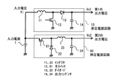
図1に示すように、1はバッテリーなどの入力電源であり、入力電圧Viを供給する。10は第1の電源回路である昇圧電源回路であり、入力電圧Viを昇圧して第1の出力電圧Vo1を出力する。昇圧電源回路10は、入力電圧Viを供給する入力電源1に接続されたインダクタ11、インダクタ11の他端に接続されたNMOSトランジスタからなる主スイッチ12、主スイッチ12の電圧を整流平滑するダイオード13と出力コンデンサ14、第1の出力電圧Vo1を目標値に制御するように主スイッチ12をオンオフ制御する第1の制御回路15から構成される。
As shown in FIG. 1,
主スイッチ12のスイッチング動作によってインダクタ11へのエネルギーの蓄積と放出が繰り返され、主スイッチ12のオフ時においてインダクタ11からダイオード13を介して出力コンデンサ14を充電する電流が流れる。主スイッチ12の1スイッチング周期に占めるオン時間の割合をデューティ比δ1とし、ダイオード13の順方向電圧降下等を無視すると、昇圧電源回路10の出力電圧Vo1は、(数3)
By the switching operation of the
また、図1において、20は第2の電源回路である降圧電源回路であり、入力電圧Viを降圧して第2の出力電圧Vo2を出力する。降圧電源回路20は、入力電源1に入力端が接続された主スイッチ回路21、主スイッチ回路21の出力端に接続されたダイオード22、主スイッチ回路21の出力端とダイオード22の接続点電圧を平滑するインダクタ23と出力コンデンサ24、第2の出力電圧Vo2を目標値に制御するように主スイッチ回路21をオンオフ制御する第2の制御回路25から構成される。
In FIG. 1,
ここで、主スイッチ回路21は、PMOSトランジスタである第1のスイッチ素子26とNMOSトランジスタである第2のスイッチ素子27との並列構成を有し、第2の制御回路25が出力する駆動信号に従って第1のスイッチ素子26をオンオフする第1の駆動回路28と、インバータ29を介した駆動信号の反転信号に従って第2のスイッチ素子27をオンオフする第2の駆動回路30から構成される。第1の駆動回路28は入力電圧Viを電源とし、第2の駆動回路30は第1の出力電圧Vo1を電源とする。すなわち、第2のスイッチ素子27のゲート用電源として第1の出力電圧Vo1を供給する。
Here, the
図2は第1の駆動回路28と第2の駆動回路30の構成を示した主スイッチ回路21の回路構成図である。第1の駆動回路28は、第2の制御回路25の出力が「H」レベルであると、PMOSトランジスタ31がオフ、NMOSトランジスタ32がオンして第1のスイッチ素子26をオンし、第2の制御回路25の出力が「L」レベルであると、PMOSトランジスタ31がオン、NMOSトランジスタ32がオフして第1のスイッチ素子26をオフする。
FIG. 2 is a circuit configuration diagram of the
また、第2の駆動回路30は、第2の制御回路25の出力が「H」レベルであると、インバータ29を介して「L」レベルを入力され、PMOSトランジスタ33がオン、NMOSトランジスタ34がオフして第2のスイッチ素子27をオンし、第2の制御回路25の出力が「L」レベルであると、インバータ29を介して「H」レベルを入力され、PMOSトランジスタ33がオフ、NMOSトランジスタ34がオンして第2のスイッチ素子27をオフする。
Further, when the output of the
以上のように構成された本実施形態1に係る多出力電源装置の第2の電源回路(降圧電源回路20)の動作を以下に説明する。 The operation of the second power supply circuit (step-down power supply circuit 20) of the multi-output power supply device according to the first embodiment configured as described above will be described below.
第2の電源回路である降圧電源回路20の基本的な動作は従来例で説明した通りである。すなわち、主スイッチ回路21の入出力端が開閉するスイッチング動作によってインダクタ23へのエネルギーの蓄積と放出が繰り返され、主スイッチ回路21のオフ期間中にインダクタ23を介して出力コンデンサ24を充電する電流が流れる。主スイッチ回路21の1スイッチング周期に占めるオン時間の割合をデューティ比δ2とし、ダイオード22の順方向電圧降下等を無視すると、降圧電源回路20の第2の出力電圧Vo2は、(数4)
The basic operation of the step-down
![]()
![]()
まず、入力電圧Viが低い時、PMOSトランジスタである第1のスイッチ素子26のオン抵抗は、ゲート電圧が不足するため大きくなる。しかし、NMOSトランジスタである第2のスイッチ素子27は、オン時において、第1の出力電圧Vo1からゲート電圧を供給され、そのゲート−ソース間電圧には、第1の出力電圧Vo1と入力電圧Viとの差電圧(Vo1−Vi)が印加される。このため入力電圧Viが低いほど高いゲート−ソース間電圧が得られて小さなオン抵抗となり、主スイッチ回路21は低いオン電圧でスイッチング動作することができる。
First, when the input voltage Vi is low, the on-resistance of the
次に、入力電圧Viが高い時、NMOSトランジスタである第2のスイッチ素子27は、ゲート−ソース間電圧(Vo1−Vi)が低くなるのでオン抵抗が大きくなる。しかし、PMOSトランジスタである第1のスイッチ素子26のオン抵抗は、そのソース−ゲート間電圧に入力電圧Viが印加されるため小さくなり、主スイッチ回路21は低いオン電圧でスイッチング動作することができる。
Next, when the input voltage Vi is high, the
以上のように本実施形態1の多出力電源装置の第2の電源回路である降圧電源回路20は、入力電圧Viの高低にかかわらず、主スイッチ回路21が低いオン電圧でスイッチング動作することができる。しかも主スイッチ回路21を構成する第2のスイッチ素子27へのゲート用電源電圧は、第1の電源回路である昇圧電源回路10によって安定化制御された第1の出力電圧Vo1であり、耐圧を越える危険性はない。
As described above, in the step-down
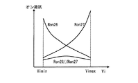
なお、図3に第1のスイッチ素子26のオン抵抗Ron26と、第2のスイッチ素子27のオン抵抗Ron27と、オン抵抗Ron26とオン抵抗Ron27の並列抵抗(Ron26//Ron27)が入力電圧Viによって変化する様子を示す。PMOSトランジスタである第1のスイッチ素子26のオン抵抗は、ソース−ゲート間電圧が入力電圧Viであるので、入力電圧Viが低いほどオン抵抗は大きくなる。一方、NMOSトランジスタである第2のスイッチ素子27は、ゲート−ソース間電圧が第1の出力電圧Vo1と入力電圧Viとの差電圧(Vo1−Vi)であるので、入力電圧Viが高いほどオン抵抗は大きくなる。この両者の並列抵抗が主スイッチ回路21のオン抵抗となる。主スイッチ回路21のオン抵抗が入力電圧Viによる変動の少ない安定な抵抗値を示すには、入力電圧Viの最小時における第2のスイッチ素子27のオン抵抗Ron27と、入力電圧Viの最大時における第1のスイッチ素子26のオン抵抗Ron26が、ほぼ等しくなるように各スイッチのトランジスタサイズを設定すればよい。
In FIG. 3, the on-resistance Ron26 of the
(実施形態2)
図4は本発明の実施形態2に係る多出力電源装置の回路構成図であり、前述の実施形態1における降圧電源回路20として構成した第2の電源回路を第3の電源回路(反転電源回路40)で構成したものである。図4に示すように、第3の電源回路の反転電源回路40は、入力電圧Viを反転昇降圧して第3の出力電圧Vo3を出力する。
(Embodiment 2)
FIG. 4 is a circuit configuration diagram of a multi-output power supply device according to Embodiment 2 of the present invention. The second power supply circuit configured as the step-down
反転電源回路40は、入力電源1に入力端が接続された主スイッチ回路41、主スイッチ回路41の出力端に接続されたインダクタ42、主スイッチ回路41の出力端とインダクタ42の接続点にカソードが接続されたダイオード43、ダイオード43のアノードに接続されて平滑する出力コンデンサ44、第3の出力電圧Vo3を目標値に制御するように主スイッチ回路41をオンオフ制御する第3の制御回路45から構成される。
The inverting
ここで、主スイッチ回路41は、PMOSトランジスタである第1のスイッチ素子46とNMOSトランジスタである第2のスイッチ素子47との並列構成を有し、第3の制御回路45が出力する駆動信号に従って第1のスイッチ素子46をオンオフする第1の駆動回路48と、インバータ49を介して駆動信号の反転信号に従って第2のスイッチ素子47をオンオフする第2の駆動回路50から構成される。第1の駆動回路48は入力電圧Viを電源とし、第2の駆動回路50は第1の出力電圧Vo1を電源とする。すなわち、第2のスイッチ素子47のゲート用電源として第1の出力電圧Vo1を供給する。
Here, the
主スイッチ回路41の入出力端が開閉するスイッチング動作によってインダクタ42へのエネルギーの蓄積と放出が繰り返され、主スイッチ回路41のオフ期間中にインダクタ42を介して出力コンデンサ44を充電する電流が流れる。主スイッチ回路41の1スイッチング周期に占めるオン時間の割合をデューティ比δ3とし、ダイオード43の順方向電圧降下等を無視すると、反転電源回路40の第3の出力電圧Vo3は、(数5)
By the switching operation in which the input / output terminal of the
主スイッチ回路41の構成は前述の実施形態1の主スイッチ回路21の構成と同様であり、その動作も同様である。すなわち、入力電圧Viが低い時、第1のスイッチ素子46のオン抵抗は大きくなるが、NMOSトランジスタである第2のスイッチ素子47は、そのゲート−ソース間電圧に第1の出力電圧Vo1と入力電圧Viとの差電圧(Vo1−Vi)が印加されるので、入力電圧Viが低いほど小さなオン抵抗となる。
The configuration of the
次に、入力電圧Viが高い時、第2のスイッチ素子47はオン抵抗が大きくなるが、PMOSトランジスタである第1のスイッチ素子46のオン抵抗は小さくなる。結果、主スイッチ回路41は入力電圧Viの高低にかかわらず、低いオン電圧でスイッチング動作することができる。しかも主スイッチ回路41を構成する第2のスイッチ素子47へのゲート用電源電圧は、第1の電源回路である昇圧電源回路10によって安定化制御された第1の出力電圧Vo1であり、耐圧を越える危険性はない。
Next, when the input voltage Vi is high, the on-resistance of the
本発明に係る多出力電源装置は、昇圧電源回路を含む多出力電源装置において、広範な入力電圧範囲で高効率な動作をする降圧電源回路や反転電源回路を構成でき、多出力電源として有用である。 The multi-output power supply device according to the present invention can constitute a step-down power supply circuit and an inverting power supply circuit that operate efficiently in a wide input voltage range in a multi-output power supply device including a boost power supply circuit, and is useful as a multi-output power supply. is there.
1 入力電源
10 昇圧電源回路
11,23,42 インダクタ
12,61,71 主スイッチ
13,22,43,74,76 ダイオード
14,24,44 出力コンデンサ
15 第1の制御回路
21 主スイッチ回路
25 第2の制御回路
26,46 第1のスイッチ素子
27,47 第2のスイッチ素子
28,48 第1の駆動回路
29,49 インバータ
30,50 第2の駆動回路
45 第3の制御回路
60,70 降圧電源回路
72 昇圧インダクタ
73 昇圧スイッチ
75 ゲート電源コンデンサ
77 制御部
1
Claims (5)
前記第2の電源回路の主スイッチ回路は、制御端子を低電位側に引かれることでオン状態となる第1のスイッチ素子と、制御端子を高電位側に引かれることでオン状態となる第2のスイッチ素子との並列構成を有し、前記第2のスイッチ素子の制御端子への印加電圧源を前記第1の電源回路の第1の出力電圧とすることを特徴とする多出力電源装置。 A first power supply circuit that boosts an input voltage supplied from an input power supply and outputs a first output voltage, and a second output voltage is output from the input voltage via a main switch circuit connected to the input power supply. A second power supply circuit,
The main switch circuit of the second power supply circuit includes a first switch element that is turned on when the control terminal is pulled to the low potential side, and a first switch element that is turned on when the control terminal is pulled to the high potential side. A multi-output power supply device having a parallel configuration with two switch elements, wherein the voltage source applied to the control terminal of the second switch element is the first output voltage of the first power supply circuit .
Priority Applications (2)
| Application Number | Priority Date | Filing Date | Title |
|---|---|---|---|
| JP2006264025A JP4753826B2 (en) | 2006-09-28 | 2006-09-28 | Multi-output power supply |
| US11/902,880 US7586212B2 (en) | 2006-09-28 | 2007-09-26 | Multi-output power supply apparatus |
Applications Claiming Priority (1)
| Application Number | Priority Date | Filing Date | Title |
|---|---|---|---|
| JP2006264025A JP4753826B2 (en) | 2006-09-28 | 2006-09-28 | Multi-output power supply |
Publications (2)
| Publication Number | Publication Date |
|---|---|
| JP2008086133A JP2008086133A (en) | 2008-04-10 |
| JP4753826B2 true JP4753826B2 (en) | 2011-08-24 |
Family
ID=39356410
Family Applications (1)
| Application Number | Title | Priority Date | Filing Date |
|---|---|---|---|
| JP2006264025A Expired - Fee Related JP4753826B2 (en) | 2006-09-28 | 2006-09-28 | Multi-output power supply |
Country Status (2)
| Country | Link |
|---|---|
| US (1) | US7586212B2 (en) |
| JP (1) | JP4753826B2 (en) |
Families Citing this family (4)
| Publication number | Priority date | Publication date | Assignee | Title |
|---|---|---|---|---|
| US8044536B2 (en) * | 2007-10-10 | 2011-10-25 | Ams Research Corporation | Powering devices having low and high voltage circuits |
| CN102005919B (en) * | 2009-09-02 | 2014-03-12 | 瑞萨集成电路设计(北京)有限公司 | Boost DC-DC (Direct Current-Direct Current) converter and method |
| ES2692372T3 (en) * | 2010-11-22 | 2018-12-03 | Saab Ab | Arrangement of energy supply for energy distribution |
| JP6031883B2 (en) * | 2012-08-08 | 2016-11-24 | 富士通株式会社 | Semiconductor integrated circuit and power supply circuit |
Family Cites Families (8)
| Publication number | Priority date | Publication date | Assignee | Title |
|---|---|---|---|---|
| JPS5834494Y2 (en) * | 1977-06-18 | 1983-08-03 | ソニー株式会社 | power circuit |
| US4644251A (en) * | 1985-04-01 | 1987-02-17 | Motorola, Inc. | Dual voltage tracking control device |
| JP3000633B2 (en) * | 1990-07-18 | 2000-01-17 | セイコーエプソン株式会社 | Electronics |
| JPH07222439A (en) | 1994-02-02 | 1995-08-18 | Fuji Electric Co Ltd | Dc-dc converter |
| JP2005117886A (en) | 2003-09-19 | 2005-04-28 | Matsushita Electric Ind Co Ltd | Multiple-output dc-dc converter |
| JP4201205B2 (en) | 2004-06-15 | 2008-12-24 | パナソニック株式会社 | Multi-output power supply circuit and electronic device using the same |
| JP2006014910A (en) | 2004-07-01 | 2006-01-19 | Akihiko Maeda | Cleaning net |
| JP4832240B2 (en) * | 2006-09-29 | 2011-12-07 | パナソニック株式会社 | Multi-output power supply |
-
2006
- 2006-09-28 JP JP2006264025A patent/JP4753826B2/en not_active Expired - Fee Related
-
2007
- 2007-09-26 US US11/902,880 patent/US7586212B2/en active Active
Also Published As
| Publication number | Publication date |
|---|---|
| US7586212B2 (en) | 2009-09-08 |
| JP2008086133A (en) | 2008-04-10 |
| US20080179950A1 (en) | 2008-07-31 |
Similar Documents
| Publication | Publication Date | Title |
|---|---|---|
| JP5297116B2 (en) | Booster circuit and power supply device using the same | |
| JP4781744B2 (en) | POWER SUPPLY DEVICE AND ELECTRIC DEVICE USING THE SAME | |
| US20120091978A1 (en) | Dc-dc converter | |
| JP2010110070A (en) | Dc-dc converter | |
| US9667144B2 (en) | DC-DC converter with reverse current detecting circuit | |
| JP2010004692A (en) | Flashing power supply device | |
| JP5866920B2 (en) | Switching device and control method thereof | |
| JP5098760B2 (en) | DC-DC converter and power supply control semiconductor integrated circuit | |
| JP2012253953A (en) | Step-up dc-dc converter | |
| JP5157603B2 (en) | Boost DC-DC converter and power source driving semiconductor integrated circuit | |
| JP2010004691A (en) | Flashing power supply device | |
| JP2007244086A (en) | Soft start circuit of switching power supply | |
| JP4753826B2 (en) | Multi-output power supply | |
| JP2009022092A (en) | Multi-output power supply circuit | |
| JP2008060492A (en) | Light-emitting device drive | |
| JP5951358B2 (en) | Charging control circuit and charging circuit | |
| US8159089B2 (en) | Power supply circuit and semiconductor device for use therein | |
| JP2014011841A (en) | Switching regulator | |
| JP2007089333A (en) | Step-up/down converter | |
| US10333400B2 (en) | Boost DC-DC converter including a switching element | |
| JP2008166076A (en) | Electronic equipment system and power source control method | |
| JP6409171B2 (en) | Switching power supply device, electronic device, and bidirectional DCDC converter | |
| US20090058385A1 (en) | Step-up DC-DC converter | |
| WO2023153085A1 (en) | Charging/discharging device and charging/discharging control method | |
| JP2010259198A (en) | Dc-dc conversion apparatus |
Legal Events
| Date | Code | Title | Description |
|---|---|---|---|
| A621 | Written request for application examination |
Free format text: JAPANESE INTERMEDIATE CODE: A621 Effective date: 20081203 |
|
| RD03 | Notification of appointment of power of attorney |
Free format text: JAPANESE INTERMEDIATE CODE: A7423 Effective date: 20100917 |
|
| RD04 | Notification of resignation of power of attorney |
Free format text: JAPANESE INTERMEDIATE CODE: A7424 Effective date: 20100927 |
|
| A977 | Report on retrieval |
Free format text: JAPANESE INTERMEDIATE CODE: A971007 Effective date: 20110420 |
|
| TRDD | Decision of grant or rejection written | ||
| A01 | Written decision to grant a patent or to grant a registration (utility model) |
Free format text: JAPANESE INTERMEDIATE CODE: A01 Effective date: 20110426 |
|
| A61 | First payment of annual fees (during grant procedure) |
Free format text: JAPANESE INTERMEDIATE CODE: A61 Effective date: 20110524 |
|
| FPAY | Renewal fee payment (event date is renewal date of database) |
Free format text: PAYMENT UNTIL: 20140603 Year of fee payment: 3 |
|
| R151 | Written notification of patent or utility model registration |
Ref document number: 4753826 Country of ref document: JP Free format text: JAPANESE INTERMEDIATE CODE: R151 |
|
| FPAY | Renewal fee payment (event date is renewal date of database) |
Free format text: PAYMENT UNTIL: 20140603 Year of fee payment: 3 |
|
| S111 | Request for change of ownership or part of ownership |
Free format text: JAPANESE INTERMEDIATE CODE: R313113 |
|
| R350 | Written notification of registration of transfer |
Free format text: JAPANESE INTERMEDIATE CODE: R350 |
|
| R250 | Receipt of annual fees |
Free format text: JAPANESE INTERMEDIATE CODE: R250 |
|
| R250 | Receipt of annual fees |
Free format text: JAPANESE INTERMEDIATE CODE: R250 |
|
| LAPS | Cancellation because of no payment of annual fees |