JP4711895B2 - 光電フレキシブル配線板の接続構造、並びにコネクタ及び光電フレキシブル配線板 - Google Patents
光電フレキシブル配線板の接続構造、並びにコネクタ及び光電フレキシブル配線板 Download PDFInfo
- Publication number
- JP4711895B2 JP4711895B2 JP2006165020A JP2006165020A JP4711895B2 JP 4711895 B2 JP4711895 B2 JP 4711895B2 JP 2006165020 A JP2006165020 A JP 2006165020A JP 2006165020 A JP2006165020 A JP 2006165020A JP 4711895 B2 JP4711895 B2 JP 4711895B2
- Authority
- JP
- Japan
- Prior art keywords
- wiring board
- flexible wiring
- photoelectric flexible
- connector
- photoelectric
- Prior art date
- Legal status (The legal status is an assumption and is not a legal conclusion. Google has not performed a legal analysis and makes no representation as to the accuracy of the status listed.)
- Active
Links
- 230000003287 optical effect Effects 0.000 claims description 183
- 230000005540 biological transmission Effects 0.000 claims description 117
- 239000000758 substrate Substances 0.000 claims description 31
- 238000006243 chemical reaction Methods 0.000 claims description 11
- 238000005452 bending Methods 0.000 claims description 5
- 230000010365 information processing Effects 0.000 claims description 4
- 238000010276 construction Methods 0.000 claims 1
- 239000011347 resin Substances 0.000 description 10
- 229920005989 resin Polymers 0.000 description 10
- 230000006866 deterioration Effects 0.000 description 7
- 238000010586 diagram Methods 0.000 description 4
- 230000008054 signal transmission Effects 0.000 description 4
- 238000004519 manufacturing process Methods 0.000 description 3
- RYGMFSIKBFXOCR-UHFFFAOYSA-N Copper Chemical compound [Cu] RYGMFSIKBFXOCR-UHFFFAOYSA-N 0.000 description 2
- 230000001413 cellular effect Effects 0.000 description 1
- 238000004891 communication Methods 0.000 description 1
- 229910052802 copper Inorganic materials 0.000 description 1
- 239000010949 copper Substances 0.000 description 1
- 238000011161 development Methods 0.000 description 1
- 238000003780 insertion Methods 0.000 description 1
- 230000037431 insertion Effects 0.000 description 1
- 238000000034 method Methods 0.000 description 1
- 238000000465 moulding Methods 0.000 description 1
- 230000005693 optoelectronics Effects 0.000 description 1
Images


Classifications
-
- G—PHYSICS
- G02—OPTICS
- G02B—OPTICAL ELEMENTS, SYSTEMS OR APPARATUS
- G02B6/00—Light guides; Structural details of arrangements comprising light guides and other optical elements, e.g. couplings
- G02B6/24—Coupling light guides
- G02B6/42—Coupling light guides with opto-electronic elements
- G02B6/43—Arrangements comprising a plurality of opto-electronic elements and associated optical interconnections
-
- H—ELECTRICITY
- H01—ELECTRIC ELEMENTS
- H01R—ELECTRICALLY-CONDUCTIVE CONNECTIONS; STRUCTURAL ASSOCIATIONS OF A PLURALITY OF MUTUALLY-INSULATED ELECTRICAL CONNECTING ELEMENTS; COUPLING DEVICES; CURRENT COLLECTORS
- H01R12/00—Structural associations of a plurality of mutually-insulated electrical connecting elements, specially adapted for printed circuits, e.g. printed circuit boards [PCB], flat or ribbon cables, or like generally planar structures, e.g. terminal strips, terminal blocks; Coupling devices specially adapted for printed circuits, flat or ribbon cables, or like generally planar structures; Terminals specially adapted for contact with, or insertion into, printed circuits, flat or ribbon cables, or like generally planar structures
- H01R12/70—Coupling devices
- H01R12/77—Coupling devices for flexible printed circuits, flat or ribbon cables or like structures
- H01R12/78—Coupling devices for flexible printed circuits, flat or ribbon cables or like structures connecting to other flexible printed circuits, flat or ribbon cables or like structures
-
- G—PHYSICS
- G02—OPTICS
- G02B—OPTICAL ELEMENTS, SYSTEMS OR APPARATUS
- G02B6/00—Light guides; Structural details of arrangements comprising light guides and other optical elements, e.g. couplings
- G02B6/10—Light guides; Structural details of arrangements comprising light guides and other optical elements, e.g. couplings of the optical waveguide type
-
- G—PHYSICS
- G02—OPTICS
- G02B—OPTICAL ELEMENTS, SYSTEMS OR APPARATUS
- G02B6/00—Light guides; Structural details of arrangements comprising light guides and other optical elements, e.g. couplings
- G02B6/24—Coupling light guides
- G02B6/42—Coupling light guides with opto-electronic elements
- G02B6/4201—Packages, e.g. shape, construction, internal or external details
- G02B6/4204—Packages, e.g. shape, construction, internal or external details the coupling comprising intermediate optical elements, e.g. lenses, holograms
- G02B6/4214—Packages, e.g. shape, construction, internal or external details the coupling comprising intermediate optical elements, e.g. lenses, holograms the intermediate optical element having redirecting reflective means, e.g. mirrors, prisms for deflecting the radiation from horizontal to down- or upward direction toward a device
-
- G—PHYSICS
- G02—OPTICS
- G02B—OPTICAL ELEMENTS, SYSTEMS OR APPARATUS
- G02B6/00—Light guides; Structural details of arrangements comprising light guides and other optical elements, e.g. couplings
- G02B6/24—Coupling light guides
- G02B6/42—Coupling light guides with opto-electronic elements
- G02B6/4292—Coupling light guides with opto-electronic elements the light guide being disconnectable from the opto-electronic element, e.g. mutually self aligning arrangements
-
- G—PHYSICS
- G02—OPTICS
- G02B—OPTICAL ELEMENTS, SYSTEMS OR APPARATUS
- G02B6/00—Light guides; Structural details of arrangements comprising light guides and other optical elements, e.g. couplings
- G02B6/24—Coupling light guides
- G02B6/36—Mechanical coupling means
- G02B6/38—Mechanical coupling means having fibre to fibre mating means
- G02B6/3807—Dismountable connectors, i.e. comprising plugs
- G02B6/381—Dismountable connectors, i.e. comprising plugs of the ferrule type, e.g. fibre ends embedded in ferrules, connecting a pair of fibres
- G02B6/3817—Dismountable connectors, i.e. comprising plugs of the ferrule type, e.g. fibre ends embedded in ferrules, connecting a pair of fibres containing optical and electrical conductors
-
- G—PHYSICS
- G02—OPTICS
- G02B—OPTICAL ELEMENTS, SYSTEMS OR APPARATUS
- G02B6/00—Light guides; Structural details of arrangements comprising light guides and other optical elements, e.g. couplings
- G02B6/24—Coupling light guides
- G02B6/36—Mechanical coupling means
- G02B6/38—Mechanical coupling means having fibre to fibre mating means
- G02B6/3807—Dismountable connectors, i.e. comprising plugs
- G02B6/3897—Connectors fixed to housings, casing, frames or circuit boards
Description
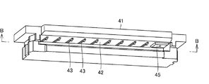
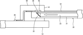
20 電子機器の蓋体
11,21 筐体
12,22 実装基板(リジット基板)
30 光電フレキシブル配線板
31 板状ベース
32 電気伝送路
33 光伝送路
36 信号入出口
40,50 コネクタ
41 ボディ
42 ガイド穴
43 コンタクト
45,55 光素子
60,70 ドライバー
Claims (10)
- 光信号と電気信号の両方を伝送する光電フレキシブル配線板を、コネクタを用いて基板に接続する光電フレキシブル配線板の接続構造であって、
前記コネクタは、前記光電フレキシブル配線板の端部が挿入可能な断面凹状のガイド穴と、
前記ガイド穴の天井面に幅方向に配列された複数のコンタクトと、
前記ガイド穴の天井面に設けられた光素子とを備えており、
前記基板には前記コネクタ及び光電変換可能な前記光素子のドライバーが実装されており、
前記光電フレキシブル配線板は、その表面上における前記コンタクトに各々接触可能な位置に幅方向に配設されており且つ全長が光電フレキシブル配線板の全長と略同じである複数の電気伝送路と、
内部に設けられており且つ全長が光電フレキシブル配線板の全長と略同じである光伝送路と、
前記端部表面における前記光素子に対向可能な位置に設けられた光信号入出口と、
前記光伝送路の端部内における前記光信号入出口に対向した位置に配設されており且つ当該光導波路を直角に曲げるための導波路ミラーとを備えていることを特徴とする光電フレキシブル配線板の接続構造。 - 請求項1記載の光電フレキシブル配線板の接続構造において、
前記光素子が前記コンタクトの配列方向の最も外側に配置されており、
前記光伝送路が前記電気伝送路の配列方向の最も外側に配置されていることを特徴とする光電フレキシブル配線板の接続構造。 - 請求項1記載の光電フレキシブル配線板の接続構造において、
前記コネクタは、ガイド穴の長さ方向の両端部に各々設けられた一対の凸部を更に備えており、
前記光電フレキシブル配線板は、前記端部の両端部に各々設けられており且つ前記凸部に嵌合可能な凹状の一対の固定部を更に備えていることを特徴とする光電フレキシブル配線板の接続構造。 - 請求項1記載の光電フレキシブル配線板の接続構造において、
前記コネクタは、前記光電フレキシブル配線板の端部が前記ガイド穴に挿入された状態で固定するスライダを更に備えていることを特徴とする光電フレキシブル配線板の接続構造。 - 請求項1記載の光電フレキシブル配線板の接続構造において、
本体と、表示部を兼ねる蓋体と、前記本体と前記蓋体とを回動自在に連結するヒンジ軸とを備えた情報処理端末装置に適用されるものであり、
前記本体は、前記基板である本体側の実装基板と、前記コネクタである本体側のコネクタとを備え、
前記蓋体は、前記基板である蓋体側の実装基板と、前記コネクタである蓋体側のコネクタとを備え、
前記光電フレキシブル配線板は、前記本体側のコネクタのガイド穴に挿入可能な一方の端部と、前記蓋体側のコネクタのガイド穴に挿入可能な他方の端部とを備えていることを特徴とする光電フレキシブル配線板の接続構造。 - 請求項1記載の光電フレキシブル配線板の接続構造に用いられるコネクタにおいて、
前記光電フレキシブル配線板の端部が挿入可能な断面凹状のガイド穴が設けられたボディと、
前記ボディのガイド穴の天井面に前記光電フレキシブル配線板の表面上の前記電気伝送路に各々対応して幅方向に配列された複数のコンタクトと、
前記ボディのガイド穴の天井面における前記光電フレキシブル配線板の表面上の光信号入出口に対向可能な位置に配設された前記光素子とを備えており、
前記コンタクトは、前記ボディに埋設された中間部と、前記ガイド穴の天井面から露出する一端部と、前記ボディの背面から突出し前記基板に接続される他端部とを有していることを特徴とするコネクタ。 - 請求項6記載のコネクタにおいて、
前記光素子が前記コンタクトの配列方向の最も外側に配置されていることを特徴とするコネクタ。 - 請求項1記載の光電フレキシブル配線板の接続構造に用いられる光電フレキシブル配線板において、
端部が前記コネクタのガイド穴に挿入可能な板状ベースと、
前記板状ベースの表面上における前記コンタクトに各々接触可能な位置に幅方向に配設されており且つ全長が光電フレキシブル配線板の全長と略同じである複数の電気伝送路と、
前記板状ベースの内部に設けられており且つ全長が光電フレキシブル配線板の全長と略同じである光伝送路と、
前記板状ベースの端部表面における前記光素子に対向可能な位置に設けられた光信号入出口と、
前記光伝送路の端部内における前記光信号入出口に対向した位置に配設されており且つ当該光導波路を直角に曲げるための導波路ミラーとを備えることを特徴とする光電フレキシブル配線板。 - 請求項8記載の光電フレキシブル配線板において、
前記光伝送路が前記電気伝送路の配列方向の最も外側に配置されていることを特徴とする光電フレキシブル配線板。 - 請求項9に記載の光電フレキシブル配線板において、
前記板状ベースの両端部には、一対のコネクタのガイド穴の両端部に各々設けられた一対の凸部が各々嵌合して当該板状ベースの抜け止めをする一対の固定部が設けられていることを特徴とする光電フレキシブル配線板。
Priority Applications (7)
| Application Number | Priority Date | Filing Date | Title |
|---|---|---|---|
| JP2006165020A JP4711895B2 (ja) | 2006-02-03 | 2006-06-14 | 光電フレキシブル配線板の接続構造、並びにコネクタ及び光電フレキシブル配線板 |
| TW096101939A TWI390740B (zh) | 2006-02-03 | 2007-01-18 | Photoelectric flexible patch panel connection structure, connector and photoelectric flexible wiring board |
| CN2007800043715A CN101379662B (zh) | 2006-02-03 | 2007-01-29 | 光电挠性布线板的连接结构及连接器和光电挠性布线板 |
| PCT/JP2007/051369 WO2007088805A1 (ja) | 2006-02-03 | 2007-01-29 | 光電フレキシブル配線板の接続構造、並びにコネクタ及び光電フレキシブル配線板 |
| EP07707600.8A EP1986278B1 (en) | 2006-02-03 | 2007-01-29 | Connection structure of photoelectric flexible wiring board, connector and photoelectric flexible wiring board |
| KR1020087018239A KR101274547B1 (ko) | 2006-02-03 | 2007-01-29 | 광전 플렉서블 배선판의 접속 구조, 커넥터 및 광전플렉서블 배선판 |
| US12/162,870 US7780359B2 (en) | 2006-02-03 | 2007-01-29 | Connection structure of photoelectric flexible wiring board, connector and photoelectric flexible wiring board |
Applications Claiming Priority (3)
| Application Number | Priority Date | Filing Date | Title |
|---|---|---|---|
| JP2006027689 | 2006-02-03 | ||
| JP2006027689 | 2006-02-03 | ||
| JP2006165020A JP4711895B2 (ja) | 2006-02-03 | 2006-06-14 | 光電フレキシブル配線板の接続構造、並びにコネクタ及び光電フレキシブル配線板 |
Publications (3)
| Publication Number | Publication Date |
|---|---|
| JP2007233325A JP2007233325A (ja) | 2007-09-13 |
| JP2007233325A5 JP2007233325A5 (ja) | 2008-07-17 |
| JP4711895B2 true JP4711895B2 (ja) | 2011-06-29 |
Family
ID=38327380
Family Applications (1)
| Application Number | Title | Priority Date | Filing Date |
|---|---|---|---|
| JP2006165020A Active JP4711895B2 (ja) | 2006-02-03 | 2006-06-14 | 光電フレキシブル配線板の接続構造、並びにコネクタ及び光電フレキシブル配線板 |
Country Status (7)
| Country | Link |
|---|---|
| US (1) | US7780359B2 (ja) |
| EP (1) | EP1986278B1 (ja) |
| JP (1) | JP4711895B2 (ja) |
| KR (1) | KR101274547B1 (ja) |
| CN (1) | CN101379662B (ja) |
| TW (1) | TWI390740B (ja) |
| WO (1) | WO2007088805A1 (ja) |
Families Citing this family (19)
| Publication number | Priority date | Publication date | Assignee | Title |
|---|---|---|---|---|
| US7684663B2 (en) * | 2007-11-02 | 2010-03-23 | National Semiconductor Corporation | Coupling of optical interconnect with electrical device |
| US7627204B1 (en) * | 2007-11-02 | 2009-12-01 | National Semiconductor Corporation | Optical-electrical flex interconnect using a flexible waveguide and flexible printed circuit board substrate |
| JP5211940B2 (ja) * | 2008-08-29 | 2013-06-12 | 日立化成株式会社 | 光導波路、光電気混載基板及び光モジュール |
| KR101023137B1 (ko) * | 2008-10-27 | 2011-03-23 | 한국광기술원 | 광전 혼합 커넥터를 이용한 광전배선 기판 연결장치 |
| JP5199479B2 (ja) | 2008-10-31 | 2013-05-15 | ヒューレット−パッカード デベロップメント カンパニー エル.ピー. | 構成を変更可能なコンピュータバス |
| KR20110089408A (ko) | 2008-11-21 | 2011-08-08 | 히다치 가세고교 가부시끼가이샤 | 광전기 혼재기판 및 전자기기 |
| JP5386999B2 (ja) * | 2009-01-15 | 2014-01-15 | 日立化成株式会社 | 光モジュール及び電気接続方法 |
| JP4920723B2 (ja) * | 2009-05-14 | 2012-04-18 | シャープ株式会社 | 画像表示装置用伝送システムおよび電子機器 |
| JP2011095333A (ja) * | 2009-10-27 | 2011-05-12 | Toshiba Corp | 実装構造体 |
| US8620122B2 (en) * | 2010-09-10 | 2013-12-31 | Avago Technologies General Ip (Singapore) Pte. Ltd. | Low-profile optical communications module having two generally flat optical connector modules that slidingly engage one another |
| JP5382237B2 (ja) | 2010-11-05 | 2014-01-08 | 株式会社村田製作所 | コネクタ |
| KR101266616B1 (ko) | 2011-11-29 | 2013-05-22 | 엘에스엠트론 주식회사 | 광전 배선 모듈 |
| CN103428997A (zh) * | 2012-05-23 | 2013-12-04 | 鸿富锦精密工业(深圳)有限公司 | 光电电路板及电路板模块 |
| JP2016143018A (ja) * | 2015-02-05 | 2016-08-08 | ソニー株式会社 | 光送信装置、光受信装置、及び光ケーブル |
| WO2017003474A1 (en) * | 2015-07-01 | 2017-01-05 | Intel Corporation | Fpc connector for better signal integrity and design compaction |
| KR101924939B1 (ko) * | 2017-02-24 | 2018-12-04 | 주식회사 지파랑 | 슬림형 커넥터 플러그, 이를 이용한 액티브 광 케이블 조립체 및 그의 제조방법 |
| JP6661733B1 (ja) * | 2018-11-28 | 2020-03-11 | 株式会社フジクラ | ケーブル及び画像伝送システム |
| DE102019003842A1 (de) * | 2019-06-03 | 2020-12-03 | Karl Storz Se & Co. Kg | Endoskop sowie Verfahren zur Herstellung eines Endoskops |
| JP7137274B2 (ja) * | 2019-08-02 | 2022-09-14 | ヒロセ電機株式会社 | コネクタ組立体配置構造 |
Family Cites Families (21)
| Publication number | Priority date | Publication date | Assignee | Title |
|---|---|---|---|---|
| US4678264A (en) * | 1983-03-30 | 1987-07-07 | Amp Incorporated | Electrical and fiber optic connector assembly |
| US5125054A (en) * | 1991-07-25 | 1992-06-23 | Motorola, Inc. | Laminated polymer optical waveguide interface and method of making same |
| US5396573A (en) * | 1993-08-03 | 1995-03-07 | International Business Machines Corporation | Pluggable connectors for connecting large numbers of electrical and/or optical cables to a module through a seal |
| JP3705873B2 (ja) * | 1996-10-17 | 2005-10-12 | 株式会社アドバンテスト | 光・電気混在配線板 |
| CA2272751A1 (en) * | 1996-12-31 | 1998-07-09 | Honeywell Inc. | Flexible optic connector assembly |
| US6690845B1 (en) * | 1998-10-09 | 2004-02-10 | Fujitsu Limited | Three-dimensional opto-electronic modules with electrical and optical interconnections and methods for making |
| JP4164947B2 (ja) * | 1999-06-25 | 2008-10-15 | 凸版印刷株式会社 | 光・電気配線基板及び製造方法並びに実装基板 |
| JP2001042171A (ja) * | 1999-07-28 | 2001-02-16 | Canon Inc | アクティブ光配線装置 |
| JP3331409B2 (ja) * | 1999-08-02 | 2002-10-07 | 日本航空電子工業株式会社 | 光電複合型コネクタ |
| JP2001311846A (ja) * | 2000-04-28 | 2001-11-09 | Oki Printed Circuit Kk | 電気配線・光配線混載多層シートの製造方法及び電気配線・光配線混載多層基板の製造方法 |
| US7101091B2 (en) * | 2001-02-21 | 2006-09-05 | Zarlink Semiconductor, Inc. | Apparatus for coupling a fiber optic cable to an optoelectronic device, a system including the apparatus, and a method of forming the same |
| JP2003227951A (ja) * | 2002-02-05 | 2003-08-15 | Canon Inc | 光導波装置、その製造方法、およびそれを用いた光電気混載基板 |
| EP1286194A3 (en) | 2001-08-21 | 2004-05-19 | Canon Kabushiki Kaisha | Optical waveguide apparatus |
| US6882762B2 (en) * | 2001-09-27 | 2005-04-19 | Intel Corporation | Waveguide in a printed circuit board and method of forming the same |
| US7156690B2 (en) * | 2002-01-07 | 2007-01-02 | Bernard R Tolmie | Extruded connector without channel insulating layer |
| WO2003100486A1 (fr) * | 2002-05-28 | 2003-12-04 | Matsushita Electric Works, Ltd. | Materiau pour le montage mixte de substrat de circuit optique/circuit electrique et montage mixte de substrat de circuit optique/circuit electrique |
| JP2004031508A (ja) | 2002-06-24 | 2004-01-29 | Nec Corp | 光電気複合モジュールおよびそのモジュールを構成要素とする光入出力装置 |
| JP2004191564A (ja) * | 2002-12-10 | 2004-07-08 | Mitsubishi Electric Corp | 光路変換コネクタ |
| JP2005300930A (ja) | 2004-04-12 | 2005-10-27 | Matsushita Electric Works Ltd | 光電気混載基板の製造方法 |
| US7458732B2 (en) * | 2004-12-22 | 2008-12-02 | Panasonic Electric Works Co., Ltd. | Optical and electrical compound connector |
| JP2007033688A (ja) * | 2005-07-25 | 2007-02-08 | Fuji Xerox Co Ltd | 光導波路フィルム、及び光送受信モジュール |
-
2006
- 2006-06-14 JP JP2006165020A patent/JP4711895B2/ja active Active
-
2007
- 2007-01-18 TW TW096101939A patent/TWI390740B/zh active
- 2007-01-29 KR KR1020087018239A patent/KR101274547B1/ko active IP Right Grant
- 2007-01-29 EP EP07707600.8A patent/EP1986278B1/en not_active Expired - Fee Related
- 2007-01-29 US US12/162,870 patent/US7780359B2/en active Active
- 2007-01-29 CN CN2007800043715A patent/CN101379662B/zh not_active Expired - Fee Related
- 2007-01-29 WO PCT/JP2007/051369 patent/WO2007088805A1/ja active Search and Examination
Also Published As
| Publication number | Publication date |
|---|---|
| TW200735384A (en) | 2007-09-16 |
| KR20080098008A (ko) | 2008-11-06 |
| US20090041408A1 (en) | 2009-02-12 |
| EP1986278A1 (en) | 2008-10-29 |
| EP1986278A4 (en) | 2012-04-11 |
| CN101379662A (zh) | 2009-03-04 |
| TWI390740B (zh) | 2013-03-21 |
| US7780359B2 (en) | 2010-08-24 |
| WO2007088805A1 (ja) | 2007-08-09 |
| EP1986278B1 (en) | 2016-11-16 |
| JP2007233325A (ja) | 2007-09-13 |
| KR101274547B1 (ko) | 2013-06-13 |
| CN101379662B (zh) | 2011-12-14 |
Similar Documents
| Publication | Publication Date | Title |
|---|---|---|
| JP4711895B2 (ja) | 光電フレキシブル配線板の接続構造、並びにコネクタ及び光電フレキシブル配線板 | |
| US7645075B2 (en) | Optical connection structure of optical backplane to circuit substrate | |
| US7585119B2 (en) | Optical connection structure between optical backplane and circuit substrate | |
| JP4322276B2 (ja) | 携帯電話機および電子機器 | |
| JP2007233325A5 (ja) | ||
| KR100904604B1 (ko) | 다극 커넥터 및 다극 커넥터를 사용한 휴대형 무선단말또는 소형 전자기기 | |
| US20120183264A1 (en) | Optical connector | |
| JP5290074B2 (ja) | 光コネクタ | |
| US7374426B2 (en) | Card-edge board connector that electrically connects two boards | |
| CN100536492C (zh) | 一种具有直线型软性印刷电路板的移动通信终端 | |
| KR100976654B1 (ko) | 광 인쇄회로기판 및 그 제조 방법 | |
| JP4344328B2 (ja) | 光電気複合型コネクタ | |
| KR100790714B1 (ko) | Isp를 갖는 카메라 모듈 패키지 | |
| KR102420029B1 (ko) | 플랫 케이블용 커넥터 | |
| KR200394725Y1 (ko) | 거치대용 입출력플러그의 인쇄회로기판에 대한 실장 구조 | |
| KR200360118Y1 (ko) | Usb 플러그 유니트 | |
| KR20080086258A (ko) | 듀얼 카메라 모듈의 제조 방법 | |
| KR100725483B1 (ko) | 플랫 케이블용 커넥터 | |
| KR102191370B1 (ko) | 플랫 케이블용 커넥터 | |
| CN115207723A (zh) | 一种连接器和通信设备 | |
| US20110159724A1 (en) | Wire insertion and connection structure | |
| KR101460764B1 (ko) | 기판 어셈블리 및 이를 구비한 기판 모듈 | |
| EP1811610A1 (en) | Pin holder structure of input/output plug | |
| JP2008066395A (ja) | 両面接続が可能なフレキシブルプリント基板および該基板接続用コネクタ装置 | |
| KR19980701594A (ko) | 전기 커넥터 어셈블리(electrical connector assembly) |
Legal Events
| Date | Code | Title | Description |
|---|---|---|---|
| A521 | Request for written amendment filed |
Free format text: JAPANESE INTERMEDIATE CODE: A523 Effective date: 20080603 |
|
| A621 | Written request for application examination |
Free format text: JAPANESE INTERMEDIATE CODE: A621 Effective date: 20090325 |
|
| TRDD | Decision of grant or rejection written | ||
| A01 | Written decision to grant a patent or to grant a registration (utility model) |
Free format text: JAPANESE INTERMEDIATE CODE: A01 Effective date: 20110322 |
|
| A61 | First payment of annual fees (during grant procedure) |
Free format text: JAPANESE INTERMEDIATE CODE: A61 Effective date: 20110322 |
|
| R150 | Certificate of patent or registration of utility model |
Ref document number: 4711895 Country of ref document: JP Free format text: JAPANESE INTERMEDIATE CODE: R150 |