EP1986278B1 - Connection structure of photoelectric flexible wiring board, connector and photoelectric flexible wiring board - Google Patents
Connection structure of photoelectric flexible wiring board, connector and photoelectric flexible wiring board Download PDFInfo
- Publication number
- EP1986278B1 EP1986278B1 EP07707600.8A EP07707600A EP1986278B1 EP 1986278 B1 EP1986278 B1 EP 1986278B1 EP 07707600 A EP07707600 A EP 07707600A EP 1986278 B1 EP1986278 B1 EP 1986278B1
- Authority
- EP
- European Patent Office
- Prior art keywords
- wiring board
- flexible wiring
- photoelectric flexible
- connector
- end portion
- Prior art date
- Legal status (The legal status is an assumption and is not a legal conclusion. Google has not performed a legal analysis and makes no representation as to the accuracy of the status listed.)
- Expired - Fee Related
Links
- 230000005540 biological transmission Effects 0.000 claims description 121
- 230000003287 optical effect Effects 0.000 claims description 105
- 239000011347 resin Substances 0.000 claims description 23
- 229920005989 resin Polymers 0.000 claims description 23
- 230000010365 information processing Effects 0.000 claims description 9
- 238000005452 bending Methods 0.000 claims description 4
- 230000008878 coupling Effects 0.000 claims 1
- 238000010168 coupling process Methods 0.000 claims 1
- 238000005859 coupling reaction Methods 0.000 claims 1
- 238000006243 chemical reaction Methods 0.000 description 9
- 230000001413 cellular effect Effects 0.000 description 5
- 230000015556 catabolic process Effects 0.000 description 4
- 238000006731 degradation reaction Methods 0.000 description 4
- 238000004519 manufacturing process Methods 0.000 description 3
- RYGMFSIKBFXOCR-UHFFFAOYSA-N Copper Chemical compound [Cu] RYGMFSIKBFXOCR-UHFFFAOYSA-N 0.000 description 2
- 230000001419 dependent effect Effects 0.000 description 2
- 230000008054 signal transmission Effects 0.000 description 2
- 238000013459 approach Methods 0.000 description 1
- 238000004891 communication Methods 0.000 description 1
- 229910052802 copper Inorganic materials 0.000 description 1
- 239000010949 copper Substances 0.000 description 1
- 230000006866 deterioration Effects 0.000 description 1
- 230000000694 effects Effects 0.000 description 1
- 230000007717 exclusion Effects 0.000 description 1
- 238000003780 insertion Methods 0.000 description 1
- 230000037431 insertion Effects 0.000 description 1
- 238000000034 method Methods 0.000 description 1
- 238000000465 moulding Methods 0.000 description 1
- 230000000717 retained effect Effects 0.000 description 1
Images


Classifications
-
- G—PHYSICS
- G02—OPTICS
- G02B—OPTICAL ELEMENTS, SYSTEMS OR APPARATUS
- G02B6/00—Light guides; Structural details of arrangements comprising light guides and other optical elements, e.g. couplings
- G02B6/24—Coupling light guides
- G02B6/42—Coupling light guides with opto-electronic elements
- G02B6/43—Arrangements comprising a plurality of opto-electronic elements and associated optical interconnections
-
- H—ELECTRICITY
- H01—ELECTRIC ELEMENTS
- H01R—ELECTRICALLY-CONDUCTIVE CONNECTIONS; STRUCTURAL ASSOCIATIONS OF A PLURALITY OF MUTUALLY-INSULATED ELECTRICAL CONNECTING ELEMENTS; COUPLING DEVICES; CURRENT COLLECTORS
- H01R12/00—Structural associations of a plurality of mutually-insulated electrical connecting elements, specially adapted for printed circuits, e.g. printed circuit boards [PCB], flat or ribbon cables, or like generally planar structures, e.g. terminal strips, terminal blocks; Coupling devices specially adapted for printed circuits, flat or ribbon cables, or like generally planar structures; Terminals specially adapted for contact with, or insertion into, printed circuits, flat or ribbon cables, or like generally planar structures
- H01R12/70—Coupling devices
- H01R12/77—Coupling devices for flexible printed circuits, flat or ribbon cables or like structures
- H01R12/78—Coupling devices for flexible printed circuits, flat or ribbon cables or like structures connecting to other flexible printed circuits, flat or ribbon cables or like structures
-
- G—PHYSICS
- G02—OPTICS
- G02B—OPTICAL ELEMENTS, SYSTEMS OR APPARATUS
- G02B6/00—Light guides; Structural details of arrangements comprising light guides and other optical elements, e.g. couplings
- G02B6/10—Light guides; Structural details of arrangements comprising light guides and other optical elements, e.g. couplings of the optical waveguide type
-
- G—PHYSICS
- G02—OPTICS
- G02B—OPTICAL ELEMENTS, SYSTEMS OR APPARATUS
- G02B6/00—Light guides; Structural details of arrangements comprising light guides and other optical elements, e.g. couplings
- G02B6/24—Coupling light guides
- G02B6/42—Coupling light guides with opto-electronic elements
- G02B6/4201—Packages, e.g. shape, construction, internal or external details
- G02B6/4204—Packages, e.g. shape, construction, internal or external details the coupling comprising intermediate optical elements, e.g. lenses, holograms
- G02B6/4214—Packages, e.g. shape, construction, internal or external details the coupling comprising intermediate optical elements, e.g. lenses, holograms the intermediate optical element having redirecting reflective means, e.g. mirrors, prisms for deflecting the radiation from horizontal to down- or upward direction toward a device
-
- G—PHYSICS
- G02—OPTICS
- G02B—OPTICAL ELEMENTS, SYSTEMS OR APPARATUS
- G02B6/00—Light guides; Structural details of arrangements comprising light guides and other optical elements, e.g. couplings
- G02B6/24—Coupling light guides
- G02B6/42—Coupling light guides with opto-electronic elements
- G02B6/4292—Coupling light guides with opto-electronic elements the light guide being disconnectable from the opto-electronic element, e.g. mutually self aligning arrangements
-
- G—PHYSICS
- G02—OPTICS
- G02B—OPTICAL ELEMENTS, SYSTEMS OR APPARATUS
- G02B6/00—Light guides; Structural details of arrangements comprising light guides and other optical elements, e.g. couplings
- G02B6/24—Coupling light guides
- G02B6/36—Mechanical coupling means
- G02B6/38—Mechanical coupling means having fibre to fibre mating means
- G02B6/3807—Dismountable connectors, i.e. comprising plugs
- G02B6/381—Dismountable connectors, i.e. comprising plugs of the ferrule type, e.g. fibre ends embedded in ferrules, connecting a pair of fibres
- G02B6/3817—Dismountable connectors, i.e. comprising plugs of the ferrule type, e.g. fibre ends embedded in ferrules, connecting a pair of fibres containing optical and electrical conductors
-
- G—PHYSICS
- G02—OPTICS
- G02B—OPTICAL ELEMENTS, SYSTEMS OR APPARATUS
- G02B6/00—Light guides; Structural details of arrangements comprising light guides and other optical elements, e.g. couplings
- G02B6/24—Coupling light guides
- G02B6/36—Mechanical coupling means
- G02B6/38—Mechanical coupling means having fibre to fibre mating means
- G02B6/3807—Dismountable connectors, i.e. comprising plugs
- G02B6/3897—Connectors fixed to housings, casing, frames or circuit boards
Definitions
- the present invention relates to a connection structure of a photoelectric flexible wiring board transmitting both optical and electrical signals, for connecting the wiring board to another board such as a rigid board.
- the invention also relates to a connector and a photoelectric flexible wiring board for use in the connection structure of the photoelectric flexible wiring board.
- optical-electrical mixed circuit boards which transmit both optical and electrical signals with a single board.
- the feature of the optical-electrical mixed circuit board resides in the parallel arrangement of an optical transmission line relative to a plurality of electrical transmission lines.
- Patent Documents 1 to 3 a photoelectric flexible wiring board with high flexibility has been proposed.
- a photoelectric flexible wiring board is used in information processing terminal apparatus with a rotating portion to connect an electric circuit on the main body side with an electric circuit on the cover body side.
- information processing terminal apparatuses include cellular phones, PDAs (personal digital assistants), personal computers, and game consoles.
- the photoelectric flexible wiring board is connected between a rigid mounting board on the main body side and a rigid mounting board on the cover body side, using a set of connectors. More specifically, opposite end portions of the photoelectric flexible wiring board are inserted into a set of plug-type connectors that are mounted on the mounting boards on the opposite sides, so that the flexible board is connected to the mounting boards on the opposite sides.
- FIG. 13 illustrates a conventional example of a connection structure of a photoelectric flexible wiring board.
- A denotes a main body of, e.g., a clamshell cellular phone
- B denotes a cover body of the cellular phone.
- a rigid mounting board 1a in the main body A and a rigid mounting board 1b in the cover body B are connected via a photoelectric flexible wiring board 2.
- the photoelectric flexible wiring board 2 includes a plurality of electrical transmission lines 6 and an optical transmission line 7 (an optical waveguide), as well as photonic devices 3 for converting optical signals to electrical signals and drivers 4 therefor toward the ends of the wiring board.
- the mounting boards 1a and 1b are mounted with plug-type connectors 5 and 5, into which respective end portions of the photoelectric flexible wiring board 2 are inserted, so that the mounting boards 1a and 1b are connected with each other via the photoelectric flexible wiring board 2.
- Conductive contacts that are equal in total number to the transmission lines are disposed inside the respective connectors 5 and 5 and on the opposite end portions of the photoelectric flexible wiring board 2.
- the conventional photoelectric flexible wiring board 2 performs optical transmission on the wiring board, taking in and out of signals between the wiring board and the mounting boards has to be performed in the form of electrical signals in order to interface the wiring board with the mounting boards 1a and 1b connected thereto.
- the photoelectric flexible wiring board 2 is provided on its opposite end portions with the photonic devices 3 performing photoelectric conversion and the drivers 4 therefor.
- Such a conventional photoelectric flexible wiring board 2 and its connection structure have problems as described below in connection with the mounting of the photonic devices 3 and drivers 4 therefor on the opposite end portions of the wiring board.
- the photoelectric flexible wiring board 2 compared with the entire length L1 of the photoelectric flexible wiring board 2, the length L2 of the optical transmission section in the photoelectric flexible wiring board 2, i.e., the substantial length of the optical transmission line, is relatively short. Therefore, the photoelectric flexible wiring board 2 has an unnecessarily large size, because of which its application to small apparatuses is difficult. This is the first problem.
- the photoelectric flexible wiring board 2 As the mounting portions on the ends mounted with the photonic devices 3 and drivers 4 therefor are extremely less flexible than the portion used as the optical transmission section, its original flexibility has to be secured between the photonic devices 3, resulting in overall flexibility being not as high as expected from the entire length. For this reason, it is difficult to apply the flexible wiring board 2 to such a use requiring high flexibility as clamshell cellular phones. This is the second problem.
- the third problem is increased costs for the photoelectric flexible wiring board 2 due to a process of mounting the photonic devices 3 and drivers 4 therefor in fabrication of the board 2.
- the fourth problem is that the substantial length of the optical transmission line is limited in comparison with the entire length L1 of the photoelectric flexible wiring board 2. More particularly, the optical transmission line is not present on the opposite end portions (farther portions from the photonic devices 3) of the photoelectric flexible wiring board 2. Instead, these portions have the electrical transmission lines (copper wire patterns), which transmit high-speed digital signals that should be transmitted optically. Therefore, advantages of optical transmission are not fully utilized. Specifically, these electrical transmission lines disadvantageously cause deterioration in electromagnetic compatibility (EMC) characteristics, degradation in signal transmission characteristics, and the like.
- EMC electromagnetic compatibility
- the present invention provides a connection structure for connecting a photoelectric flexible wiring board board, and the to a mounting board.
- the connection structure, a connector and the wiring board are aimed at securing a longest possible length for an optical transmission line in the photoelectric flexible wiring board, thereby allowing for downsizing of the photoelectric flexible wiring board as well as securing high flexibility and good optical transmission characteristics.
- connection structure for connecting a photoelectric flexible wiring board to a mounting board according to the present invention is defined in claim 1.
- the optical transmission line can be laid from a first end to a second end, i.e., across the substantially entire length, of the wiring board.
- the length of the optical transmission line that is useful in high-speed transmission and is highly flexible is not sacrificed for the photonic device and driver, and the optical transmission line can be made to have a longest possible length.
- the photonic device removed from the photoelectric flexible wiring board is mounted in the connector, so that photoelectric conversion can be performed similarly as in the case where the photonic device is mounted on the photoelectric flexible wiring board, without causing any functional problem.
- the driver can be mounted in the connector together with the photonic device, it is possible to mount the driver on another board on which the connector is mounted, from the aspect of avoiding increase in complexity of the wiring structure and increase in size of the connector, and the like.
- the position to dispose the photonic device in the connector is dependent on the wiring pattern of the electrical and optical transmission lines in the photoelectric flexible wiring board; therefore, when the optical transmission line is disposed in the middle of the wiring board, then the photonic device is mounted at the center in the connector, and when the optical transmission line is disposed along a lateral edge, i.e., outside the electrical transmission line group, then the photonic device is mounted at the corresponding lateral end in the connector.
- the photonic device is mounted in a lateral end portion in the connector, which portion is not sandwiched between conductive terminals (contacts), the space inside the connector can be efficiently used.
- a connector features: a body including the guide hole of U-shape in cross section, the guide hole being adapted to receive the end portion of the photoelectric flexible wiring board; the plurality of contacts, arranged laterally on the ceiling of the guide hole of the body such that the contacts correspond to the respective electrical transmission lines on the surface of the photoelectric flexible wiring board; and the photonic device, disposed on the ceiling of the guide hole of the body so as to face the optical signal entrance-cum-exit in the surface of the photoelectric flexible wiring board.
- Each of the contacts includes a middle portion embedded in the body, a first end portion exposed from the ceiling of the guide hole, and a second end portion protruded from a rear surface of the body for connection with to the board.
- the photonic device that performs photoelectric conversion is mounted at the position corresponding to the optical transmission line in the photoelectric flexible wiring board, the photonic device and driver therefor can be removed from the photoelectric flexible wiring board; therefore, the wiring board and the optical transmission line can be made substantially equal in length to each other, and it is possible to avoid a situation where the length of the optical transmission line that is useful in high-speed transmission and is highly flexible is sacrificed for the photonic device and driver.
- the connector is preferably a plug-type connector provided with a guide hole that receives an end portion of the photoelectric flexible wiring board in such a way that the optical transmission line in the photoelectric flexible wiring board is aligned with the photonic device in the connector upon reception of the end portion.
- the position to dispose the photonic device in the connector is dependent on the wiring pattern of the electrical and optical transmission lines in the photoelectric flexible wiring board; therefore, when the optical transmission line is disposed in the middle of the wiring board, then the photonic device is mounted at the center in the connector, and when the optical transmission line is disposed at an edge, i.e., outside the electrical transmission line group, then the photonic device is mounted at the corresponding lateral end in the connector.
- the photonic device is mounted in a lateral end portion in the connector, which portion is not sandwiched between conductive terminals (contacts), the space inside the connector can be efficiently used.
- a photoelectric flexible wiring board features: a plate-like base having an end portion receivable in the guide hole of the connector; the plurality of electrical transmission lines, arranged laterally on a surface of the plate-like base so as to be contactable with the respective contacts, the electrical transmission lines having the entire length substantially equal to the entire length of the photoelectric flexible wiring board; the optical transmission line, provided within the plate-like base and having the entire length substantially equal to the entire length of the photoelectric flexible wiring board; the optical signal entrance-cum-exit, provided in a surface of the end portion of the plate-like base so as to face the photonic device; and the waveguide mirror, disposed in the end portion of the optical transmission line so as to face the optical signal entrance-cum-exit, for bending the optical waveguide at a right angle.
- the transmission line for optical signals extends from the first end to the second end of the wiring board.
- the entire length of the photoelectric flexible wiring board is therefore substantially equal to the length of the optical transmission line.
- high-speed digital signals are delivered from the first end to the second end of the wiring board through the optical signal transmission line. Consequently, the wiring board can avoid a situation where high-speed digital signals pass through the electrical transmission line on the wiring board.
- An end portion of the plate-like base is specifically a portion to be inserted into the connector.
- the above wiring board structure can be achieved by mounting the photonic device and the driver in the connector.
- the plate-like base may be provided on end portions thereof with pairs of fixing portions for retaining the plate-like base by engaging with respective pairs of projections provided in the guide holes of the contacts in pair.
- the fixing portions prevent the photoelectric flexible wiring board from being accidentally detached from the connectors.
- the photonic device and driver therefor that are associated with the photoelectric flexible wiring board are removed from the photoelectric flexible wiring board, and the photonic device is mounted in the connector, so that the length of the optical transmission line can be extended to a length almost equal to the entire length of the wiring board.
- the photoelectric flexible wiring board can therefore be reduced in size in securing a necessary length for the optical transmission line, and the wiring board can easily be applied to small devices.
- the photoelectric flexible wiring board is improved in flexibility, and the manufacturing costs thereof can be reduced.
- the wiring board can maintain the optical transmission characteristics, providing an effective measure for electromagnetic compatibility (EMC) and against degradation of signals.
- EMC electromagnetic compatibility
- the connector for the photoelectric flexible wiring board according to the present invention is mounted with the photonic device at a position corresponding to the optical transmission line in the photoelectric flexible wiring board, the photonic device and the driver therefor can be removed from the photoelectric flexible wiring board.
- the length of the optical transmission line in the photoelectric flexible wiring board can be extended to a length substantially equal to the entire length of the wiring board, so that the photoelectric flexible wiring board can be reduced in size in securing a necessary length for the optical transmission line and can be easily applied to small devices.
- the exclusion of the less flexible mounting portions from the photoelectric flexible wiring board increases the flexibility of the photoelectric flexible wiring board, and the manufacturing costs thereof can thus be reduced.
- the wiring board can maintain the optical transmission characteristics, providing an effective measure for EMC and against degradation of signals.
- the end portions thereof does not have mounting portions for the photonic devices and the drivers therefor, both the optical and electrical transmission lines extend up to the ends of the board, and the signal entrance-cum-exits for the both kinds of signals are provided at the ends of the respective transmission lines. Therefore, the wiring board is highly flexible, and the width of the board can be reduced. Because the wiring board does not handle conversion from optical signals to electrical signals, avoiding a situation where high-speed digital signals pass through the electrical transmission lines, the photoelectric flexible wiring board can maintain EMC characteristics and transmission characteristics for high-speed digital signals.
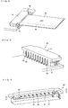
- FIG. 1 is a schematic configuration view illustrating a background example of a wiring structure of a photoelectric flexible wiring board
- FIG. 2 is a perspective view of the photoelectric flexible wiring board and a connector in use in the wiring structure of FIG. 1
- FIG. 3 is a perspective view of the connector in use as viewed from the rear side thereof
- FIG. 4 is a perspective view of the connector as viewed from the front side thereof
- FIG. 5 is a transverse cross-sectional plan view of the connector, viewed along arrows A-A in FIG. 4 .
- a wiring structure of a background example of a photoelectric flexible wiring board is used in information processing terminal apparatus with a rotating portion to connect an electric circuit in a main body 10 with an electric circuit in a cover body 20.
- information processing terminal apparatuses include cellular phones, PDAs (personal digital assistants), personal computers, and game consoles.
- the main body 10 contains a mounting board 12 in its housing 11, and the cover body 20 that is rotatably coupled to the main body 10 also contains a mounting board 22 in its housing 21, as in the main body 10.
- the mounting board 12 on the main body side and the mounting board 22 on the cover body side are both rigid boards, which are connected by means of a photoelectric flexible wiring board 30 so as not to hinder the rotational movement of the main body 10 and the cover body 20.
- plug-type connectors 40 and 50 are mounted at opposed ends of the mounting boards 12 and 22.
- the photoelectric flexible wiring board 30 includes a flexible plate-like base 31, a plurality of electrical transmission lines 32 printed in parallel with one another using copper or the like on a surface of the plate-like base 31, and an optical transmission line 33 embedded along the electrical transmission lines 32 in the plate-like base 31.
- the electrical transmission lines 32 are arranged at predetermined spacing in a lateral direction of the plate-like base 31, each extending across the entire length of the plate-like base 31.
- a key feature of the photoelectric flexible wiring board 30 is the structure of the optical transmission line 33.
- the optical transmission line 33 is provided outside the rows of the electrical transmission lines 32 continuously and in parallel thereto over the entire length of the plate-like base 31.
- a photonic device that performs photoelectric conversion and a driver therefor are excluded from the photoelectric flexible wiring board 30. That is, the optical transmission line 33 is continuously provided from one end to the other end of the photoelectric flexible wiring board. Signal inlets/outlets at ends of the optical transmission line are exposed and opened into opposite end faces of the photoelectric flexible wiring board 30.
- the connectors 40 and 50 are plug types having substantially the same structure, which structure will be described referring to FIGS. 2 to 5 with respect to one of the connectors 40.
- the connector 40 has a horizontally long, rectangular resin body 41 with a longer lateral width than the lateral width of the photoelectric flexible wiring board 30.
- the resin body 41 is provided in its front face with a horizontally long guide hole 42 to receive an end portion of the photoelectric flexible wiring board 30.
- contacts 43 that are equal in number to the electrical transmission lines 32 on the photoelectric flexible wiring board 30 are provided through insert molding.
- the plurality of contacts 43 correspond to the plurality of electrical transmission lines 32 on the photoelectric flexible wiring board 30 and are provided in the resin body 41 at the same spacings as those of the electrical transmission lines 32.
- each contact 43 projects linearly frontward along the ceiling of the guide hole 42 so as to function as a contact terminal to pressingly contact each of the electrical transmission line 32 on the upper surface of the end portion of the photoelectric flexible wiring board 30 when its end portion is inserted in the guide hole 42.
- the other end portion of each contact 43 projects in an L-shape from the rear side of the resin body 41 to function as a contact terminal to be mounted and fixed on the mounting board 12 and to be connected with an electric circuit on the mounting board 12.
- a photonic device 45 that performs photoelectric conversion is so provided as to correspond to the optical transmission line 33 in the photoelectric flexible wiring board 30.
- the photonic device 45 is located at a lateral end in the resin body 41, more specifically, outside the plurality of contacts 43, because the optical transmission line 33 is at a lateral edge of the photoelectric flexible wiring board (outside the rows of the electrical transmission lines).
- the photonic device 45 is disposed in the back of the guide hole 42 facing the front so that the photonic device 45 opposes a signal inlet/outlet in the end face of the optical transmission line 33 when the end portion of the photoelectric flexible wiring board 30 is received in the guide hole 42.
- a connection terminal 46 of the photonic device 45 protrudes in an L-shape from the rear side of the resin body 41 so as to be mounted and fixed on the mounting board 12 and to be connected to the electric circuit on the mounting board 12, like connection terminals of the contacts 43.
- a driver 60 to drive the photonic device 45 is provided in the connector 40 and is mounted on the mounting board 12 together with the connector 40.
- the connector 50 in the cover body 20 is also mounted at an end of the mounting board 22 and contains a photonic device 55 corresponding to the optical transmission line 33 in the photoelectric flexible wiring board 30.
- a driver 70 to drive the photonic device 55 is mounted on the mounting board 22 together with the connector 50.
- the mounting board 12 in the main body 10 of the electronic device and the mounting board 22 in the cover body 20 are connected electrically and optically through the connector 40, the photoelectric flexible wiring board 30, and the connector 50. That is, a first end portion of the photoelectric flexible wiring board 30 is plugged in the connector 40, while a second end portion is plugged in the connector 50, whereby the photoelectric flexible wiring board 30 connects between the mounting boards 12 and 22 photoelectrically.
- the first end portion of the photoelectric flexible wiring board 30 is inserted in the guide hole 42 in the connector 40, so that the respective connection terminals of the contacts 43 contact associated end portions (signal inlets/outles) of the electrical transmission lines arranged on the photoelectric flexible wiring board 30.
- the second end portion of the photoelectric flexible wiring board 30 is inserted in the guide hole in the connector 50, so that the respective connection terminals of the contacts contact associated end portions (signal inlets/outlets) of the electrical transmission lines 32 arranged on the photoelectric flexible wiring board 30.
- the first end portion of the photoelectric flexible wiring board 30 is inserted in the guide hole 42 in the connector 40, so that the associated end face (signal inlet/outlet) of the optical transmission line 33 in the photoelectric flexible wiring board 30 opposes the photonic device 45 inside the connector 40.
- the second end portion of the photoelectric flexible wiring board 30 is inserted in the guide hole in the connector 50, so that the associated end face (signal inlet/outlet) of the optical transmission line 33 in the photoelectric flexible wiring board 30 opposes the photonic device 55 inside the connector 50.
- the photonic device 45 inside the connector 40 converts electrical signals to optical signals, which are transmitted through the optical transmission line 33 in the photoelectric flexible wiring board 30 to the photonic device 55 inside the connector 50, where the optical signals are changed into electrical signals again.
- the photonic device 55 inside the connector 50 converts electrical signals to optical signals, which are transmitted through the optical transmission line 33 in the photoelectric flexible wiring board 30 to the photonic device 45 inside the connector 40, where the optical signals are changed into electrical signals again.
- the photonic devices 45 and 55 and the drivers 60 and 70 all associated with the optical transmission line 33 in the photoelectric flexible wiring board 30 are not on the photoelectric flexible wiring board 30 but mounted on the mounting boards 12 and 22.
- a freely bendable optical transmission section is provided from end to end, i.e., over the entire length, of the photoelectric flexible wiring board 30.
- the overall flexibility is thus improved as compared with the case in which the photonic devices 45 and 55 etc. impede the free bend. That is, if the length of the photoelectric flexible wiring board 30 is unchanged, then the flexibility is improved, and if the flexibility is secured to the same degree, then the length of the photoelectric flexible wiring board 30 can be reduced.
- the wiring board can maintain the optical transmission characteristics, which is very advantageous in terms of measures for EMC and against signal degradation.
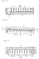
- FIG. 6 is a perspective view of a connector according to an embodiment of the present invention
- FIG. 7 is a transverse cross-sectional plan view of the connector viewed along arrows B-B in FIG. 6 .
- the present embodiment is different from the background example illustrated in FIGS. 1 to 5 in the position of the photonic device 45 in the connector 40. That is, the photonic device 45 in the embodiment illustrated in FIGS. 1 to 5 is in the back surface of the guide hole 42, i.e., in an opposed position to an end face of the inserted photoelectric flexible wiring board 30, while the photonic device 45 in the present embodiment faces the upper surface of an end portion of a photoelectric flexible wiring board 30 received in the guide hole 42, such that the photonic device 45 is disposed perpendicularly relative to the optical transmission line 33 in the photoelectric flexible wiring board 30.
- waveguide mirrors to bend optical waveguide in the wiring board 30 at a right angle are provided at opposite ends of the optical transmission line 33 in the photoelectric flexible wiring board 30, and signal inlets/outlets are open in the surface of the wiring board 30.
- connection terminal 46 of the photonic device 45 protrudes in an L-shape from the rear side of a resin body 41 so as to be mounted and fixed on the mounting board 12 and to be connected to an electric circuit on the mounting board 12, like contact terminals of contacts 43.
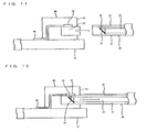
- FIG. 8 is a schematic configuration view in the form of a side view of a wiring structure of a photoelectric flexible wiring board according to another embodiment of the present invention
- FIG. 9 is a plan view of the same wiring structure
- FIG. 10 is a transverse cross-sectional plan view of the wiring structure, taken along line C-C in FIG. 8
- FIGS. 11 and 12 are longitudinal cross-sectional side views showing a positional relationship of the photoelectric flexible wiring board and a connector in the wiring structure.
- the photonic device 45 in the connector 40 is disposed perpendicularly relative to the optical transmission line 33 in the photoelectric flexible wiring board 30. More specifically, the photonic device 45 is provided facing down on the ceiling of the guide hole 42 so as to oppose the upper surface of an end portion of the photoelectric flexible wiring board 30 received in the guide hole 42.
- the photonic device 45 has its lead portion embedded in the resin body 41 and its leading end portion protruding from the rear surface at a lower end portion of the resin body 41 to follow a mounting board 12, serving as a contact terminal 46 to be mounted and fixed on the mounting board 12 and to be connected to an electric circuit on the mounting board 12, like connection terminals of contacts 43.
- a connector 50 has a similar structure to that of the connector 40.
- the photoelectric flexible wiring board 30 includes a flexible plate-like base 31.
- a plurality of electrical transmission lines 32 are printed in parallel with one another across the entire length on a surface, more specifically, on a surface excluding an edge portion, of the plate-like base 31.
- a plurality of optical transmission lines 33 are embedded in parallel with one another in the edge portion of the plate-like base 31 from a first end to a second end.
- Waveguide mirrors 35 are provided at opposite ends of the optical transmission lines 33 so as to bend optical waveguides in the optical transmission lines 33 upward at a right angle, and signal inlets/outlets 36 are open in the upper surface of the plate-like base 31.
- the signal inlets/outlets 36 of the optical transmission lines 33 oppose the photonic devices 45 and 55 when the end portions of the photoelectric flexible wiring board 30 are received in the guide hole 42 in the connector 40 and the guide hole in the connector 50, respectively.
- pairs of recessed fixing portions 39 are provided on opposite edges of either end portion of the photoelectric flexible wiring board 30.
- the pairs of recessed fixing portions 39 come in engagement with pairs of projections 49 projecting into the guide hole 42 from both sides of the connector 40 and pairs of projections 59 projecting inward in the guide hole from both sides of the connector 50, through which engagement the inserted end portions of the photoelectric flexible wiring board 30 are retained.
- the optical transmission line or lines 33 in the photoelectric flexible wiring board 30 are disposed outside the rows of the electrical transmission lines 32 and along a side edge of the wiring board, and the photonic device or devices 45 is accordingly provided at a lateral end in the connector 40.
- this position may be modified--the optical transmission line or lines 33 may be disposed on both sides of the electrical transmission lines 32 or may be disposed between the transmission lines 32.
- the optical transmission line or lines 33 are disposed outside the rows of the electrical transmission lines 32, and the photonic device or devices 45 are accordingly provided at a lateral end or lateral ends of the connector 40, space for disposing the driver or drivers 60 can be easily secured on the mounting board 12, as previously described.
- the photoelectric flexible wiring board 30 received in the connectors 40 and 50 are fixed through projection-recess engagement.
- the more security in fixing the inserted photoelectric flexible wiring board 30 increases accuracy and facility of alignment between the photonic devices 45 and 55 and the optical transmission line(s) 33.
Description
- The present invention relates to a connection structure of a photoelectric flexible wiring board transmitting both optical and electrical signals, for connecting the wiring board to another board such as a rigid board. The invention also relates to a connector and a photoelectric flexible wiring board for use in the connection structure of the photoelectric flexible wiring board.
- High-speed performance has been demanded of information processing terminal apparatuses supporting the recent high-speed communication networks. As one approach for meeting the demand, optical-electrical mixed circuit boards have been developed, which transmit both optical and electrical signals with a single board. The feature of the optical-electrical mixed circuit board resides in the parallel arrangement of an optical transmission line relative to a plurality of electrical transmission lines. As one type of such an optical-electrical mixed circuit board, a photoelectric flexible wiring board with high flexibility has been proposed (
Patent Documents 1 to 3) . -
- Patent Document 1: Japanese Unexamined Patent Publication No.
2003-227951 - Patent Document 2: Japanese Unexamined Patent Publication No.
2004-031508 - Patent Document 3: Japanese Unexamined Patent Publication No.
2005-300930 - Taking advantage of its high flexibility, a photoelectric flexible wiring board is used in information processing terminal apparatus with a rotating portion to connect an electric circuit on the main body side with an electric circuit on the cover body side. With the main body being rotatably coupled to the cover body doubling as a display by means of a hinge shaft, such information processing terminal apparatuses include cellular phones, PDAs (personal digital assistants), personal computers, and game consoles. In this case, the photoelectric flexible wiring board is connected between a rigid mounting board on the main body side and a rigid mounting board on the cover body side, using a set of connectors. More specifically, opposite end portions of the photoelectric flexible wiring board are inserted into a set of plug-type connectors that are mounted on the mounting boards on the opposite sides, so that the flexible board is connected to the mounting boards on the opposite sides.
-
FIG. 13 illustrates a conventional example of a connection structure of a photoelectric flexible wiring board. In the figure, "A" denotes a main body of, e.g., a clamshell cellular phone, and "B" denotes a cover body of the cellular phone. A rigid mounting board 1a in the main body A and arigid mounting board 1b in the cover body B are connected via a photoelectricflexible wiring board 2. The photoelectricflexible wiring board 2 includes a plurality ofelectrical transmission lines 6 and an optical transmission line 7 (an optical waveguide), as well as photonic devices 3 for converting optical signals to electrical signals and drivers 4 therefor toward the ends of the wiring board. - Meanwhile, the
mounting boards 1a and 1b are mounted with plug-type connectors flexible wiring board 2 are inserted, so that themounting boards 1a and 1b are connected with each other via the photoelectricflexible wiring board 2. Conductive contacts that are equal in total number to the transmission lines are disposed inside therespective connectors flexible wiring board 2. - That is, although the conventional photoelectric
flexible wiring board 2 performs optical transmission on the wiring board, taking in and out of signals between the wiring board and the mounting boards has to be performed in the form of electrical signals in order to interface the wiring board with themounting boards 1a and 1b connected thereto. For this reason, the photoelectricflexible wiring board 2 is provided on its opposite end portions with the photonic devices 3 performing photoelectric conversion and the drivers 4 therefor. - Such a conventional photoelectric
flexible wiring board 2 and its connection structure, however, have problems as described below in connection with the mounting of the photonic devices 3 and drivers 4 therefor on the opposite end portions of the wiring board. - That is, compared with the entire length L1 of the photoelectric
flexible wiring board 2, the length L2 of the optical transmission section in the photoelectricflexible wiring board 2, i.e., the substantial length of the optical transmission line, is relatively short. Therefore, the photoelectricflexible wiring board 2 has an unnecessarily large size, because of which its application to small apparatuses is difficult. This is the first problem. - In the photoelectric
flexible wiring board 2, as the mounting portions on the ends mounted with the photonic devices 3 and drivers 4 therefor are extremely less flexible than the portion used as the optical transmission section, its original flexibility has to be secured between the photonic devices 3, resulting in overall flexibility being not as high as expected from the entire length. For this reason, it is difficult to apply theflexible wiring board 2 to such a use requiring high flexibility as clamshell cellular phones. This is the second problem. - The third problem is increased costs for the photoelectric
flexible wiring board 2 due to a process of mounting the photonic devices 3 and drivers 4 therefor in fabrication of theboard 2. - The fourth problem is that the substantial length of the optical transmission line is limited in comparison with the entire length L1 of the photoelectric
flexible wiring board 2. More particularly, the optical transmission line is not present on the opposite end portions (farther portions from the photonic devices 3) of the photoelectricflexible wiring board 2. Instead, these portions have the electrical transmission lines (copper wire patterns), which transmit high-speed digital signals that should be transmitted optically. Therefore, advantages of optical transmission are not fully utilized. Specifically, these electrical transmission lines disadvantageously cause deterioration in electromagnetic compatibility (EMC) characteristics, degradation in signal transmission characteristics, and the like. - In view of the foregoing circumstances, the present invention provides a connection structure for connecting a photoelectric flexible wiring board board, and the to a mounting board. The connection structure, a connector and the wiring board are aimed at securing a longest possible length for an optical transmission line in the photoelectric flexible wiring board, thereby allowing for downsizing of the photoelectric flexible wiring board as well as securing high flexibility and good optical transmission characteristics.
- A connection structure for connecting a photoelectric flexible wiring board to a mounting board according to the present invention is defined in
claim 1. - In the connection structure of the photoelectric flexible wiring board according to the present invention, since the photonic device and the driver therefor, which have conventionally been disposed on an optical transmission line in the photoelectric flexible wiring board, are removed from the photoelectric flexible wiring board, the optical transmission line can be laid from a first end to a second end, i.e., across the substantially entire length, of the wiring board. In other words, the length of the optical transmission line that is useful in high-speed transmission and is highly flexible is not sacrificed for the photonic device and driver, and the optical transmission line can be made to have a longest possible length.
- The photonic device removed from the photoelectric flexible wiring board is mounted in the connector, so that photoelectric conversion can be performed similarly as in the case where the photonic device is mounted on the photoelectric flexible wiring board, without causing any functional problem. Although the driver can be mounted in the connector together with the photonic device, it is possible to mount the driver on another board on which the connector is mounted, from the aspect of avoiding increase in complexity of the wiring structure and increase in size of the connector, and the like.
- The position to dispose the photonic device in the connector is dependent on the wiring pattern of the electrical and optical transmission lines in the photoelectric flexible wiring board; therefore, when the optical transmission line is disposed in the middle of the wiring board, then the photonic device is mounted at the center in the connector, and when the optical transmission line is disposed along a lateral edge, i.e., outside the electrical transmission line group, then the photonic device is mounted at the corresponding lateral end in the connector. As in the latter case, when the photonic device is mounted in a lateral end portion in the connector, which portion is not sandwiched between conductive terminals (contacts), the space inside the connector can be efficiently used.
- Further, a connector according to the present invention features: a body including the guide hole of U-shape in cross section, the guide hole being adapted to receive the end portion of the photoelectric flexible wiring board; the plurality of contacts, arranged laterally on the ceiling of the guide hole of the body such that the contacts correspond to the respective electrical transmission lines on the surface of the photoelectric flexible wiring board; and the photonic device, disposed on the ceiling of the guide hole of the body so as to face the optical signal entrance-cum-exit in the surface of the photoelectric flexible wiring board. Each of the contacts includes a middle portion embedded in the body, a first end portion exposed from the ceiling of the guide hole, and a second end portion protruded from a rear surface of the body for connection with to the board.
- Since in the connector according to the present invention, the photonic device that performs photoelectric conversion is mounted at the position corresponding to the optical transmission line in the photoelectric flexible wiring board, the photonic device and driver therefor can be removed from the photoelectric flexible wiring board; therefore, the wiring board and the optical transmission line can be made substantially equal in length to each other, and it is possible to avoid a situation where the length of the optical transmission line that is useful in high-speed transmission and is highly flexible is sacrificed for the photonic device and driver.
- It is important in using this connector to align the optical transmission line in the photoelectric flexible wiring board connected to the connector with the photonic device mounted in the connector. For this reason, the connector is preferably a plug-type connector provided with a guide hole that receives an end portion of the photoelectric flexible wiring board in such a way that the optical transmission line in the photoelectric flexible wiring board is aligned with the photonic device in the connector upon reception of the end portion.
- The position to dispose the photonic device in the connector is dependent on the wiring pattern of the electrical and optical transmission lines in the photoelectric flexible wiring board; therefore, when the optical transmission line is disposed in the middle of the wiring board, then the photonic device is mounted at the center in the connector, and when the optical transmission line is disposed at an edge, i.e., outside the electrical transmission line group, then the photonic device is mounted at the corresponding lateral end in the connector. As in the latter case, when the photonic device is mounted in a lateral end portion in the connector, which portion is not sandwiched between conductive terminals (contacts), the space inside the connector can be efficiently used.
- Moreover, a photoelectric flexible wiring board according to the present invention features: a plate-like base having an end portion receivable in the guide hole of the connector; the plurality of electrical transmission lines, arranged laterally on a surface of the plate-like base so as to be contactable with the respective contacts, the electrical transmission lines having the entire length substantially equal to the entire length of the photoelectric flexible wiring board; the optical transmission line, provided within the plate-like base and having the entire length substantially equal to the entire length of the photoelectric flexible wiring board; the optical signal entrance-cum-exit, provided in a surface of the end portion of the plate-like base so as to face the photonic device; and the waveguide mirror, disposed in the end portion of the optical transmission line so as to face the optical signal entrance-cum-exit, for bending the optical waveguide at a right angle.
- In the photoelectric flexible wiring board according to the present invention, the transmission line for optical signals extends from the first end to the second end of the wiring board. As a result, the entire length of the photoelectric flexible wiring board is therefore substantially equal to the length of the optical transmission line. In addition, high-speed digital signals are delivered from the first end to the second end of the wiring board through the optical signal transmission line. Consequently, the wiring board can avoid a situation where high-speed digital signals pass through the electrical transmission line on the wiring board.
- An end portion of the plate-like base is specifically a portion to be inserted into the connector. As described above, the above wiring board structure can be achieved by mounting the photonic device and the driver in the connector.
- The plate-like base may be provided on end portions thereof with pairs of fixing portions for retaining the plate-like base by engaging with respective pairs of projections provided in the guide holes of the contacts in pair. The fixing portions prevent the photoelectric flexible wiring board from being accidentally detached from the connectors.
- With the connection structure of the photoelectric flexible wiring board according to the present invention, the photonic device and driver therefor that are associated with the photoelectric flexible wiring board are removed from the photoelectric flexible wiring board, and the photonic device is mounted in the connector, so that the length of the optical transmission line can be extended to a length almost equal to the entire length of the wiring board. The photoelectric flexible wiring board can therefore be reduced in size in securing a necessary length for the optical transmission line, and the wiring board can easily be applied to small devices. Moreover, by removing the less flexible mounting portions, the photoelectric flexible wiring board is improved in flexibility, and the manufacturing costs thereof can be reduced. Further, since photoelectric conversion is not performed on the photoelectric flexible wiring board, the wiring board can maintain the optical transmission characteristics, providing an effective measure for electromagnetic compatibility (EMC) and against degradation of signals.
- Because the connector for the photoelectric flexible wiring board according to the present invention is mounted with the photonic device at a position corresponding to the optical transmission line in the photoelectric flexible wiring board, the photonic device and the driver therefor can be removed from the photoelectric flexible wiring board. With this structure, the length of the optical transmission line in the photoelectric flexible wiring board can be extended to a length substantially equal to the entire length of the wiring board, so that the photoelectric flexible wiring board can be reduced in size in securing a necessary length for the optical transmission line and can be easily applied to small devices. Also, the exclusion of the less flexible mounting portions from the photoelectric flexible wiring board increases the flexibility of the photoelectric flexible wiring board, and the manufacturing costs thereof can thus be reduced. Moreover, because photoelectric conversion need not be performed on the photoelectric flexible wiring board, the wiring board can maintain the optical transmission characteristics, providing an effective measure for EMC and against degradation of signals.
- Furthermore, in the photoelectric flexible wiring board according to the present invention, the end portions thereof does not have mounting portions for the photonic devices and the drivers therefor, both the optical and electrical transmission lines extend up to the ends of the board, and the signal entrance-cum-exits for the both kinds of signals are provided at the ends of the respective transmission lines. Therefore, the wiring board is highly flexible, and the width of the board can be reduced. Because the wiring board does not handle conversion from optical signals to electrical signals, avoiding a situation where high-speed digital signals pass through the electrical transmission lines, the photoelectric flexible wiring board can maintain EMC characteristics and transmission characteristics for high-speed digital signals.
- Embodiments of the present invention will be described in detail below with reference to the drawings.
FIG. 1 is a schematic configuration view illustrating a background example of a wiring structure of a photoelectric flexible wiring board;FIG. 2 is a perspective view of the photoelectric flexible wiring board and a connector in use in the wiring structure ofFIG. 1 ;FIG. 3 is a perspective view of the connector in use as viewed from the rear side thereof,FIG. 4 is a perspective view of the connector as viewed from the front side thereof, andFIG. 5 is a transverse cross-sectional plan view of the connector, viewed along arrows A-A inFIG. 4 . - As shown in
FIG. 1 , a wiring structure of a background example of a photoelectric flexible wiring board is used in information processing terminal apparatus with a rotating portion to connect an electric circuit in amain body 10 with an electric circuit in acover body 20. With themain body 10 being rotatably coupled to thecover body 20 doubling as a display by means of a hinge shaft, such information processing terminal apparatuses include cellular phones, PDAs (personal digital assistants), personal computers, and game consoles. - The
main body 10 contains a mountingboard 12 in itshousing 11, and thecover body 20 that is rotatably coupled to themain body 10 also contains a mountingboard 22 in itshousing 21, as in themain body 10. The mountingboard 12 on the main body side and the mountingboard 22 on the cover body side are both rigid boards, which are connected by means of a photoelectricflexible wiring board 30 so as not to hinder the rotational movement of themain body 10 and thecover body 20. For this connection, plug-type connectors boards - The photoelectric
flexible wiring board 30 includes a flexible plate-like base 31, a plurality ofelectrical transmission lines 32 printed in parallel with one another using copper or the like on a surface of the plate-like base 31, and anoptical transmission line 33 embedded along theelectrical transmission lines 32 in the plate-like base 31. Theelectrical transmission lines 32 are arranged at predetermined spacing in a lateral direction of the plate-like base 31, each extending across the entire length of the plate-like base 31. - A key feature of the photoelectric
flexible wiring board 30 is the structure of theoptical transmission line 33. Theoptical transmission line 33 is provided outside the rows of theelectrical transmission lines 32 continuously and in parallel thereto over the entire length of the plate-like base 31. In this configuration, a photonic device that performs photoelectric conversion and a driver therefor are excluded from the photoelectricflexible wiring board 30. That is, theoptical transmission line 33 is continuously provided from one end to the other end of the photoelectric flexible wiring board. Signal inlets/outlets at ends of the optical transmission line are exposed and opened into opposite end faces of the photoelectricflexible wiring board 30. - The
connectors FIGS. 2 to 5 with respect to one of theconnectors 40. Theconnector 40 has a horizontally long,rectangular resin body 41 with a longer lateral width than the lateral width of the photoelectricflexible wiring board 30. Theresin body 41 is provided in its front face with a horizontallylong guide hole 42 to receive an end portion of the photoelectricflexible wiring board 30. - In the
resin body 41,contacts 43 that are equal in number to theelectrical transmission lines 32 on the photoelectricflexible wiring board 30 are provided through insert molding. The plurality ofcontacts 43 correspond to the plurality ofelectrical transmission lines 32 on the photoelectricflexible wiring board 30 and are provided in theresin body 41 at the same spacings as those of theelectrical transmission lines 32. - An end portion of each
contact 43 projects linearly frontward along the ceiling of theguide hole 42 so as to function as a contact terminal to pressingly contact each of theelectrical transmission line 32 on the upper surface of the end portion of the photoelectricflexible wiring board 30 when its end portion is inserted in theguide hole 42. The other end portion of eachcontact 43 projects in an L-shape from the rear side of theresin body 41 to function as a contact terminal to be mounted and fixed on the mountingboard 12 and to be connected with an electric circuit on the mountingboard 12. - Inside the
resin body 41, aphotonic device 45 that performs photoelectric conversion is so provided as to correspond to theoptical transmission line 33 in the photoelectricflexible wiring board 30. Thephotonic device 45 is located at a lateral end in theresin body 41, more specifically, outside the plurality ofcontacts 43, because theoptical transmission line 33 is at a lateral edge of the photoelectric flexible wiring board (outside the rows of the electrical transmission lines). Thephotonic device 45 is disposed in the back of theguide hole 42 facing the front so that thephotonic device 45 opposes a signal inlet/outlet in the end face of theoptical transmission line 33 when the end portion of the photoelectricflexible wiring board 30 is received in theguide hole 42. - A
connection terminal 46 of thephotonic device 45 protrudes in an L-shape from the rear side of theresin body 41 so as to be mounted and fixed on the mountingboard 12 and to be connected to the electric circuit on the mountingboard 12, like connection terminals of thecontacts 43. - A
driver 60 to drive thephotonic device 45 is provided in theconnector 40 and is mounted on the mountingboard 12 together with theconnector 40. - The
connector 50 in thecover body 20 is also mounted at an end of the mountingboard 22 and contains aphotonic device 55 corresponding to theoptical transmission line 33 in the photoelectricflexible wiring board 30. Adriver 70 to drive thephotonic device 55 is mounted on the mountingboard 22 together with theconnector 50. - In the wiring structure of the photoelectric flexible wiring board according to this background example, the mounting
board 12 in themain body 10 of the electronic device and the mountingboard 22 in thecover body 20 are connected electrically and optically through theconnector 40, the photoelectricflexible wiring board 30, and theconnector 50. That is, a first end portion of the photoelectricflexible wiring board 30 is plugged in theconnector 40, while a second end portion is plugged in theconnector 50, whereby the photoelectricflexible wiring board 30 connects between the mountingboards - More specifically, the first end portion of the photoelectric
flexible wiring board 30 is inserted in theguide hole 42 in theconnector 40, so that the respective connection terminals of thecontacts 43 contact associated end portions (signal inlets/outles) of the electrical transmission lines arranged on the photoelectricflexible wiring board 30. Then, the second end portion of the photoelectricflexible wiring board 30 is inserted in the guide hole in theconnector 50, so that the respective connection terminals of the contacts contact associated end portions (signal inlets/outlets) of theelectrical transmission lines 32 arranged on the photoelectricflexible wiring board 30. With this structure, electrical signals are transmitted to and fro between the mountingboards contacts 43 in theconnector 40, theelectrical transmission lines 32 on the photoelectricflexible wiring board 30, and the contacts in theconnector 50. - As for the transmission of optical signals, the first end portion of the photoelectric
flexible wiring board 30 is inserted in theguide hole 42 in theconnector 40, so that the associated end face (signal inlet/outlet) of theoptical transmission line 33 in the photoelectricflexible wiring board 30 opposes thephotonic device 45 inside theconnector 40. Then, the second end portion of the photoelectricflexible wiring board 30 is inserted in the guide hole in theconnector 50, so that the associated end face (signal inlet/outlet) of theoptical transmission line 33 in the photoelectricflexible wiring board 30 opposes thephotonic device 55 inside theconnector 50. With this structure, the respectivephotonic devices connectors optical transmission line 33 in the photoelectricflexible wiring board 30. As a result, optical signals are transmitted in the following manner. - For example, the
photonic device 45 inside theconnector 40 converts electrical signals to optical signals, which are transmitted through theoptical transmission line 33 in the photoelectricflexible wiring board 30 to thephotonic device 55 inside theconnector 50, where the optical signals are changed into electrical signals again. Alternatively, thephotonic device 55 inside theconnector 50 converts electrical signals to optical signals, which are transmitted through theoptical transmission line 33 in the photoelectricflexible wiring board 30 to thephotonic device 45 inside theconnector 40, where the optical signals are changed into electrical signals again. - As described herein, the
photonic devices drivers optical transmission line 33 in the photoelectricflexible wiring board 30 are not on the photoelectricflexible wiring board 30 but mounted on the mountingboards flexible wiring board 30. The overall flexibility is thus improved as compared with the case in which thephotonic devices flexible wiring board 30 is unchanged, then the flexibility is improved, and if the flexibility is secured to the same degree, then the length of the photoelectricflexible wiring board 30 can be reduced. - Not mounting the
photonic devices drivers flexible wiring board 30 allows reduction in the cost of mounting on the photoelectricflexible wiring board 30, leading to enhanced economic efficiency of the photoelectricflexible wiring board 30. - Also, since photoelectric conversion is not performed on the photoelectric
flexible wiring board 30, the wiring board can maintain the optical transmission characteristics, which is very advantageous in terms of measures for EMC and against signal degradation. -
FIG. 6 is a perspective view of a connector according to an embodiment of the present invention, whereasFIG. 7 is a transverse cross-sectional plan view of the connector viewed along arrows B-B inFIG. 6 . - The present embodiment is different from the background example illustrated in
FIGS. 1 to 5 in the position of thephotonic device 45 in theconnector 40. That is, thephotonic device 45 in the embodiment illustrated inFIGS. 1 to 5 is in the back surface of theguide hole 42, i.e., in an opposed position to an end face of the inserted photoelectricflexible wiring board 30, while thephotonic device 45 in the present embodiment faces the upper surface of an end portion of a photoelectricflexible wiring board 30 received in theguide hole 42, such that thephotonic device 45 is disposed perpendicularly relative to theoptical transmission line 33 in the photoelectricflexible wiring board 30. For this positional relationship, waveguide mirrors to bend optical waveguide in thewiring board 30 at a right angle are provided at opposite ends of theoptical transmission line 33 in the photoelectricflexible wiring board 30, and signal inlets/outlets are open in the surface of thewiring board 30. - The
connection terminal 46 of thephotonic device 45 protrudes in an L-shape from the rear side of aresin body 41 so as to be mounted and fixed on the mountingboard 12 and to be connected to an electric circuit on the mountingboard 12, like contact terminals ofcontacts 43. -
FIG. 8 is a schematic configuration view in the form of a side view of a wiring structure of a photoelectric flexible wiring board according to another embodiment of the present invention,FIG. 9 is a plan view of the same wiring structure,FIG. 10 is a transverse cross-sectional plan view of the wiring structure, taken along line C-C inFIG. 8 , andFIGS. 11 and 12 are longitudinal cross-sectional side views showing a positional relationship of the photoelectric flexible wiring board and a connector in the wiring structure. - In the present embodiment, as in the embodiment illustrated in
FIGS. 6 and 7 , thephotonic device 45 in theconnector 40 is disposed perpendicularly relative to theoptical transmission line 33 in the photoelectricflexible wiring board 30. More specifically, thephotonic device 45 is provided facing down on the ceiling of theguide hole 42 so as to oppose the upper surface of an end portion of the photoelectricflexible wiring board 30 received in theguide hole 42. Thephotonic device 45 has its lead portion embedded in theresin body 41 and its leading end portion protruding from the rear surface at a lower end portion of theresin body 41 to follow a mountingboard 12, serving as acontact terminal 46 to be mounted and fixed on the mountingboard 12 and to be connected to an electric circuit on the mountingboard 12, like connection terminals ofcontacts 43. Note that aconnector 50 has a similar structure to that of theconnector 40. - The photoelectric
flexible wiring board 30 includes a flexible plate-like base 31. A plurality ofelectrical transmission lines 32 are printed in parallel with one another across the entire length on a surface, more specifically, on a surface excluding an edge portion, of the plate-like base 31. A plurality ofoptical transmission lines 33 are embedded in parallel with one another in the edge portion of the plate-like base 31 from a first end to a second end. Waveguide mirrors 35 are provided at opposite ends of theoptical transmission lines 33 so as to bend optical waveguides in theoptical transmission lines 33 upward at a right angle, and signal inlets/outlets 36 are open in the upper surface of the plate-like base 31. With this structure, the signal inlets/outlets 36 of theoptical transmission lines 33 oppose thephotonic devices flexible wiring board 30 are received in theguide hole 42 in theconnector 40 and the guide hole in theconnector 50, respectively. - Also, pairs of recessed fixing
portions 39 are provided on opposite edges of either end portion of the photoelectricflexible wiring board 30. When the end portions of the photoelectricflexible wiring board 30 are inserted in theguide hole 42 in theconnector 40 and the guide hole in theconnector 50 respectively, the pairs of recessed fixingportions 39 come in engagement with pairs ofprojections 49 projecting into theguide hole 42 from both sides of theconnector 40 and pairs ofprojections 59 projecting inward in the guide hole from both sides of theconnector 50, through which engagement the inserted end portions of the photoelectricflexible wiring board 30 are retained. - In the foregoing embodiments, the optical transmission line or
lines 33 in the photoelectricflexible wiring board 30 are disposed outside the rows of theelectrical transmission lines 32 and along a side edge of the wiring board, and the photonic device ordevices 45 is accordingly provided at a lateral end in theconnector 40. However, this position may be modified--the optical transmission line orlines 33 may be disposed on both sides of theelectrical transmission lines 32 or may be disposed between thetransmission lines 32. In the case where the optical transmission line orlines 33 are disposed outside the rows of theelectrical transmission lines 32, and the photonic device ordevices 45 are accordingly provided at a lateral end or lateral ends of theconnector 40, space for disposing the driver ordrivers 60 can be easily secured on the mountingboard 12, as previously described. - In one of the foregoing embodiments, the photoelectric
flexible wiring board 30 received in theconnectors flexible wiring board 30 into the guide holes in theconnectors connectors flexible wiring board 30 increases accuracy and facility of alignment between thephotonic devices -
-
FIG. 1 is a schematic configuration view illustrating a wiring structure of a photoelectric flexible wiring board according to a background example; -
FIG. 2 is a perspective view of the photoelectric flexible wiring board and a connector in use in the wiring structured ofFIG. 1 . -
FIG. 3 is a perspective view of the connector ofFIG. 2 in use as viewed from the rear side thereof. -
FIG. 4 is a perspective view of the connector ofFIG. 2 as viewed from the front side thereof. -
FIG. 5 is a transverse cross-sectional plan view of the connector ofFIG. 2 viewed along arrows A-A inFIG. 4 . -
FIG. 6 is a perspective view of a connector according to an embodiment of the present invention. -
FIG. 7 is a transverse cross-sectional plan view of the connector viewed along arrows B-B inFIG. 6 . -
FIG. 8 is a schematic configuration view in the form of a side view of a wiring structure of a photoelectric flexible wiring board according to another embodiment of the present invention. -
FIG. 9 is a plan view of the same wiring structure. -
FIG. 10 is a transverse cross-sectional plan view of the wiring structure, taken along line C-C inFIG. 8 . -
FIG. 11 is a longitudinal cross-sectional side view showing a relationship between the photoelectric flexible wiring board and a connector in the wiring structure. -
FIG. 12 is a longitudinal cross-sectional side view showing the relationship between the photoelectric flexible wiring board and the connector in the wiring structure. -
FIG. 13 is a schematic configuration view in the form of a longitudinal cross-sectional side view of a wiring structure of a conventional photoelectric flexible wiring board. -
- 10
- main body of electronic device
- 20
- cover body of electronic device
- 11, 21
- housing
- 12, 22
- mounting board (rigid board)
- 30
- photoelectric flexible wiring board
- 31
- plate-like base
- 32
- electrical transmission line
- 33
- optical transmission line
- 36
- signal inlet/outlet
- 40, 50
- connector
- 41
- body
- 42
- guide hole
- 43
- contact
- 45, 55
- photonic device
- 60, 70
- driver
Claims (12)
- A connection structure for connecting a photoelectric flexible wiring board to a mounting board of an information processing terminal apparatus, the connection structure comprising:a connector (40, 50); anda photoelectric flexible wiring board (30) capable of transmitting opticaland electrical signals;
wherein the connector (40, 50) is adapted to be mounted, in use, to a mounting board (12, 22) of an information processing terminal apparatus, the connector comprising:a resin body (41, 51), the resin body having a guide hole (42, 52) of U-shape in cross section, the guide hole being adapted to receive an end portion of the photoelectric flexible wiring board (30);a plurality of contacts (43, 53) arranged laterally on a ceiling of the guide hole of the resin body, anda photonic device (45, 55) provided on the ceiling of the guide holeof the resin body;
and wherein the photoelectric flexible wiring board (30) comprises:a plurality of electrical transmission lines (32), arranged laterally on a surface of the photoelectric flexible wiring board so as to be contactable with the respective contacts (43, 53), the electrical transmission lines having a length substantially equal to an entire length of the photoelectric flexible wiring board;an optical transmission line (33), provided within the photoelectric flexible wiring board and having a length substantially equal to the entire length of the photoelectric flexible wiring board,an optical signal inlet/outlet (36), provided in a surface of the end portion of the photoelectric flexible wiring board (30) so as to face the photonic device (45, 55), anda waveguide mirror (35), disposed in an end portion of the optical transmission line (33) so as to face the optical signal inlet/outlet (36), for bending the optical waveguide at a right angle. - The connection structure of claim 1, whereinthe photonic device (45, 55) is disposed at an outermost position in a direction in which the contacts (43, 53) are arranged, andthe optical transmission line (33) is disposed at an outermost position in a direction in which the electrical transmission lines (32) are arranged.
- The connection structure of claim 1, whereinthe connector (40, 50) further comprises a pair of projections (49, 59) respectively provided at longitudinal opposite ends of the guide hole (42, 52), andthe photoelectric flexible wiring board (30) further comprises a pair of fixing portions (39) respectively provided at opposite edges of the end portion thereof, the fixing portions being recessed for engagement with the projections (49, 59).
- The connection structure of claim 1, whereinthe connection structure is applied to an information processing terminal apparatus including a main body (10), a cover body (20) doubling as a display, and a hinge shaft pivotally coupling the main body to the cover body,the main body (10) includes a main-body-side mounting board (12) serving as said mounting board and a main-body-side connector (40) serving as said connector,the cover body (20) includes a cover-body-side mounting board (22) serving as said mounting board and a cover-body-side connector (50) serving as said connector, andthe photoelectric flexible wiring board (30) includes a first end portion receivable in a guide hole (42) of the main-body-side connector (40) and a second end portion receivable in a guide hole (52) of the cover-body-side connector (50).
- The connection structure of claim 1, wherein each of the contacts (43, 53) includes:a middle portion embedded in the resin body (41, 51);a first end portion exposed from the ceiling of the guide hole, anda second end portion protruded from a rear surface of the resin body (41, 51) for connection to a mounting board (12, 22) of an information processing terminal apparatus, in use.
- The connection structure according to claim 5, wherein the photonic device (45, 55) is disposed at an outermost position in a direction in which the contacts (43, 53) are arranged.
- The connection structure of claim 1, wherein the photoelectric flexible wiring board (30) comprises:a plate-like base (31) having the end portion receivable in the guide hole of the connector;the plurality of electrical transmission lines (32), arranged laterally on a surface of the plate-like base (31) so as to be contactable with respective contacts (43, 53) of the connector (40, 50), the electrical transmission lines having a length substantially equal to the entire length of the photoelectric flexible wiring board (30);the optical transmission line (33), provided within the plate-like base (31) and having a length substantially equal to the entire length of the photoelectric flexible wiring board (30);the optical signal inlet/outlet (36), provided in a surface of the end portion of the plate-like base (31) so as to face the photonic device (45, 55); andthe waveguide mirror (35), disposed in the end portion of the optical transmission line (33) so as to face the optical signal inlet/outlet (36), for bending the optical waveguide at a right angle.
- The connection structure according to claim 7, wherein the optical transmission line (33) is disposed at an outermost position in a direction in which the electrical transmission lines (32) are arranged.
- The connection structure according to claim 8, wherein the plate-like base (31) of the photoelectric flexible wiring board (30) is provided on end portions thereof with pairs of fixing portions (39) for retaining the plate-like base (31) by engaging with respective pairs of projections (49, 59) provided in the guide holes (42, 52) of the connectors (40, 50).
- A connector (40, 50) for use in the connection structure of claim 1, the connector comprising:a resin body (41, 51), the resin body including a guide hole (42, 52) of U-shape in cross section, the guide hole being adapted to receive an end portion of a photoelectric flexible wiring board (30);a plurality of contacts (43, 53), arranged laterally on the ceiling of the guide hole of the resin body such that the contacts correspond to respective electrical transmission lines (32) on a surface of a photoelectric flexible wiring board (30) to which the connector is connectable, in use; anda photonic device (45, 55), disposed on the ceiling of the guide hole of the resin body so as to face an optical signal inlet/outlet (36) in the surface of the photoelectric flexible wiring board (30),wherein each of the contacts (43, 53) includes:a middle portion embedded in the resin body (41, 51),a first end portion exposed from the ceiling of the guide hole (42, 52), anda second end portion protruded from a rear surface of the resin body (41, 51) for connection with a mounting board (12, 22) on which the connector (40, 50) is mountable, in use.
- The connector (40, 50) according to claim 10, wherein the photonic device (45, 55) is disposed at an outermost position in a direction in which the contacts (43, 53) are arranged.
- A photoelectric flexible wiring board (30) for use in the connection structure of claim 1, the photoelectric flexible wiring board comprising:a plate-like base (31) having the end portion receivable in a guide hole (42, 52) of a connector (40, 50) to which the photoelectric flexible wiring board is connectable, in use;a plurality of electrical transmission lines (32), arranged laterally on a surface of the plate-like base (31) so as to be contactable with respective contacts (43, 53) of a connector (40, 50) to which the photoelectric flexible wiring board is connectable, in use, the electrical transmission lines having a length substantially equal to the entire length of the photoelectric flexible wiring board (30);an optical transmission line (33), provided within the plate-like base (31) and having a length substantially equal to the entire length of the photoelectric flexible wiring board (30);an optical signal inlet/outlet (36), provided in a surface of the end portion of the plate-like base (31) so as to face a photonic device (45, 55) of a connector (40, 50) to which the photoelectric flexible wiring board is connectable, in use; anda waveguide mirror (35), disposed in the end portion of the optical transmission line (33) so as to face the optical signal inlet/outlet (36), for bending the optical waveguide at a right angle, wherein the optical transmission line (33) is disposed at an outermost position in a direction in which the electrical transmission lines (32) are arranged,wherein the plate-like base (31) is provided on end portions thereof with pairs of fixing portions (39) for retaining the plate-like base (31) by engaging with respective pairs of projections (49, 59) provided in the guide holes (42, 52) of connectors (40, 50) to which the photoelectric flexible wiring board (30) is connectable, in use.
Applications Claiming Priority (3)
| Application Number | Priority Date | Filing Date | Title |
|---|---|---|---|
| JP2006027689 | 2006-02-03 | ||
| JP2006165020A JP4711895B2 (en) | 2006-02-03 | 2006-06-14 | Photoelectric flexible wiring board connection structure, connector and photoelectric flexible wiring board |
| PCT/JP2007/051369 WO2007088805A1 (en) | 2006-02-03 | 2007-01-29 | Connection structure of photoelectric flexible wiring board, connector and photoelectric flexible wiring board |
Publications (3)
| Publication Number | Publication Date |
|---|---|
| EP1986278A1 EP1986278A1 (en) | 2008-10-29 |
| EP1986278A4 EP1986278A4 (en) | 2012-04-11 |
| EP1986278B1 true EP1986278B1 (en) | 2016-11-16 |
Family
ID=38327380
Family Applications (1)
| Application Number | Title | Priority Date | Filing Date |
|---|---|---|---|
| EP07707600.8A Expired - Fee Related EP1986278B1 (en) | 2006-02-03 | 2007-01-29 | Connection structure of photoelectric flexible wiring board, connector and photoelectric flexible wiring board |
Country Status (7)
| Country | Link |
|---|---|
| US (1) | US7780359B2 (en) |
| EP (1) | EP1986278B1 (en) |
| JP (1) | JP4711895B2 (en) |
| KR (1) | KR101274547B1 (en) |
| CN (1) | CN101379662B (en) |
| TW (1) | TWI390740B (en) |
| WO (1) | WO2007088805A1 (en) |
Families Citing this family (19)
| Publication number | Priority date | Publication date | Assignee | Title |
|---|---|---|---|---|
| US7684663B2 (en) * | 2007-11-02 | 2010-03-23 | National Semiconductor Corporation | Coupling of optical interconnect with electrical device |
| US7627204B1 (en) * | 2007-11-02 | 2009-12-01 | National Semiconductor Corporation | Optical-electrical flex interconnect using a flexible waveguide and flexible printed circuit board substrate |
| JP5211940B2 (en) * | 2008-08-29 | 2013-06-12 | 日立化成株式会社 | Optical waveguide, opto-electric hybrid board and optical module |
| KR101023137B1 (en) * | 2008-10-27 | 2011-03-23 | 한국광기술원 | optical-electro wiring borad interconnection device using electro-optic hybrid connector |
| CN102203754B (en) * | 2008-10-31 | 2015-08-26 | 惠普开发有限公司 | The computer bus of reconfigurable |
| US9069128B2 (en) | 2008-11-21 | 2015-06-30 | Hitachi Chemical Company, Ltd. | Opto-electric combined circuit board and electronic devices |
| JP5386999B2 (en) * | 2009-01-15 | 2014-01-15 | 日立化成株式会社 | Optical module and electrical connection method |
| JP4920723B2 (en) * | 2009-05-14 | 2012-04-18 | シャープ株式会社 | Transmission system for image display device and electronic device |
| JP2011095333A (en) * | 2009-10-27 | 2011-05-12 | Toshiba Corp | Mounting structure |
| US8620122B2 (en) * | 2010-09-10 | 2013-12-31 | Avago Technologies General Ip (Singapore) Pte. Ltd. | Low-profile optical communications module having two generally flat optical connector modules that slidingly engage one another |
| KR20130061756A (en) | 2010-11-05 | 2013-06-11 | 가부시키가이샤 무라타 세이사쿠쇼 | Connector |
| KR101266616B1 (en) | 2011-11-29 | 2013-05-22 | 엘에스엠트론 주식회사 | Optical interconnection module |
| CN103428997A (en) * | 2012-05-23 | 2013-12-04 | 鸿富锦精密工业(深圳)有限公司 | Photoelectric circuit board and circuit board module |
| JP2016143018A (en) | 2015-02-05 | 2016-08-08 | ソニー株式会社 | Optical transmitter, optical receiver and optical fiber |
| DE112015006664T5 (en) * | 2015-07-01 | 2018-05-24 | Intel Corporation | FPC connectors for better signal integrity and design compaction |
| KR101924939B1 (en) | 2017-02-24 | 2018-12-04 | 주식회사 지파랑 | Slim Type Connector Plug, Active Optical Cable Assembly Using the Same and Method of Manufacturing the Same |
| JP6661733B1 (en) * | 2018-11-28 | 2020-03-11 | 株式会社フジクラ | Cable and image transmission system |
| DE102019003842A1 (en) * | 2019-06-03 | 2020-12-03 | Karl Storz Se & Co. Kg | Endoscope and method for producing an endoscope |
| JP7137274B2 (en) * | 2019-08-02 | 2022-09-14 | ヒロセ電機株式会社 | Connector assembly arrangement structure |
Citations (2)
| Publication number | Priority date | Publication date | Assignee | Title |
|---|---|---|---|---|
| US5125054A (en) * | 1991-07-25 | 1992-06-23 | Motorola, Inc. | Laminated polymer optical waveguide interface and method of making same |
| US6088498A (en) * | 1996-12-31 | 2000-07-11 | Honeywell Inc. | Flexible optic connector assembly |
Family Cites Families (19)
| Publication number | Priority date | Publication date | Assignee | Title |
|---|---|---|---|---|
| US4678264A (en) * | 1983-03-30 | 1987-07-07 | Amp Incorporated | Electrical and fiber optic connector assembly |
| US5396573A (en) * | 1993-08-03 | 1995-03-07 | International Business Machines Corporation | Pluggable connectors for connecting large numbers of electrical and/or optical cables to a module through a seal |
| JP3705873B2 (en) * | 1996-10-17 | 2005-10-12 | 株式会社アドバンテスト | Optical / electric mixed wiring board |
| US6690845B1 (en) * | 1998-10-09 | 2004-02-10 | Fujitsu Limited | Three-dimensional opto-electronic modules with electrical and optical interconnections and methods for making |
| JP4164947B2 (en) * | 1999-06-25 | 2008-10-15 | 凸版印刷株式会社 | Optical / electrical wiring board, manufacturing method, and mounting board |
| JP2001042171A (en) * | 1999-07-28 | 2001-02-16 | Canon Inc | Active optical wiring device |
| JP3331409B2 (en) * | 1999-08-02 | 2002-10-07 | 日本航空電子工業株式会社 | Photoelectric composite connector |
| JP2001311846A (en) * | 2000-04-28 | 2001-11-09 | Oki Printed Circuit Kk | Method for manufacturing electric wiring/optical wiring coexisting multilayer sheet and method for manufacturing electric wiring/optical wiring coexisting multilayer substrate |
| US7101091B2 (en) * | 2001-02-21 | 2006-09-05 | Zarlink Semiconductor, Inc. | Apparatus for coupling a fiber optic cable to an optoelectronic device, a system including the apparatus, and a method of forming the same |
| EP1286194A3 (en) | 2001-08-21 | 2004-05-19 | Canon Kabushiki Kaisha | Optical waveguide apparatus |
| JP2003227951A (en) * | 2002-02-05 | 2003-08-15 | Canon Inc | Optical waveguide device, method of manufacturing the same, and optoelectric coexisting substrate using the same |
| US6882762B2 (en) * | 2001-09-27 | 2005-04-19 | Intel Corporation | Waveguide in a printed circuit board and method of forming the same |
| US7156690B2 (en) * | 2002-01-07 | 2007-01-02 | Bernard R Tolmie | Extruded connector without channel insulating layer |
| WO2003100486A1 (en) * | 2002-05-28 | 2003-12-04 | Matsushita Electric Works, Ltd. | Material for substrate mounting optical circuit-electric circuit mixedly and substrate mounting optical circuit-electric circuit mixedly |
| JP2004031508A (en) | 2002-06-24 | 2004-01-29 | Nec Corp | Optoelectric composite module and light inputting/outputting device with its module as configuring element |
| JP2004191564A (en) * | 2002-12-10 | 2004-07-08 | Mitsubishi Electric Corp | Optical path converting connector |
| JP2005300930A (en) | 2004-04-12 | 2005-10-27 | Matsushita Electric Works Ltd | Method for manufacturing optical and electrical consolidated substrate |
| CN100432728C (en) * | 2004-12-22 | 2008-11-12 | 松下电工株式会社 | Optical/electrical composite connctor |
| JP2007033688A (en) * | 2005-07-25 | 2007-02-08 | Fuji Xerox Co Ltd | Optical waveguide film and optical transmission and reception module |
-
2006
- 2006-06-14 JP JP2006165020A patent/JP4711895B2/en active Active
-
2007
- 2007-01-18 TW TW096101939A patent/TWI390740B/en active
- 2007-01-29 EP EP07707600.8A patent/EP1986278B1/en not_active Expired - Fee Related
- 2007-01-29 CN CN2007800043715A patent/CN101379662B/en not_active Expired - Fee Related
- 2007-01-29 KR KR1020087018239A patent/KR101274547B1/en active IP Right Grant
- 2007-01-29 US US12/162,870 patent/US7780359B2/en active Active
- 2007-01-29 WO PCT/JP2007/051369 patent/WO2007088805A1/en active Search and Examination
Patent Citations (2)
| Publication number | Priority date | Publication date | Assignee | Title |
|---|---|---|---|---|
| US5125054A (en) * | 1991-07-25 | 1992-06-23 | Motorola, Inc. | Laminated polymer optical waveguide interface and method of making same |
| US6088498A (en) * | 1996-12-31 | 2000-07-11 | Honeywell Inc. | Flexible optic connector assembly |
Also Published As
| Publication number | Publication date |
|---|---|
| US7780359B2 (en) | 2010-08-24 |
| WO2007088805A1 (en) | 2007-08-09 |
| CN101379662B (en) | 2011-12-14 |
| EP1986278A1 (en) | 2008-10-29 |
| TW200735384A (en) | 2007-09-16 |
| KR101274547B1 (en) | 2013-06-13 |
| TWI390740B (en) | 2013-03-21 |
| CN101379662A (en) | 2009-03-04 |
| EP1986278A4 (en) | 2012-04-11 |
| KR20080098008A (en) | 2008-11-06 |
| JP4711895B2 (en) | 2011-06-29 |
| US20090041408A1 (en) | 2009-02-12 |
| JP2007233325A (en) | 2007-09-13 |
Similar Documents
| Publication | Publication Date | Title |
|---|---|---|
| EP1986278B1 (en) | Connection structure of photoelectric flexible wiring board, connector and photoelectric flexible wiring board | |
| KR100937274B1 (en) | Reduced size eight-pin audio jack electrical connector | |
| US7645075B2 (en) | Optical connection structure of optical backplane to circuit substrate | |
| US7585119B2 (en) | Optical connection structure between optical backplane and circuit substrate | |
| CN102623823A (en) | Thin connector assembly that has optical and electrical capabilities and that includes a plug having an optical surface that can be easily wiped clean | |
| EP2093840A1 (en) | Connector, optical transmission module and optical-electrical transmission module | |
| EP1331498A1 (en) | Optical active connector plug for lan and connector port | |
| JP4238187B2 (en) | Photoelectric composite connector and board using the same | |
| US7467953B2 (en) | Cable connector assembly with improved coupler | |
| US7175475B2 (en) | Receptacle for copper wire transceivers | |
| US9417414B2 (en) | Optical connector for a card including concave and convex guide portions | |
| US7396166B1 (en) | Optical transceiver module | |
| WO2009045366A1 (en) | Flat opto-electric hybrid connector system | |
| US7373184B2 (en) | Portable radio communication apparatus and connection member | |
| US6876809B1 (en) | Release mechanism for disconnecting internal fiber from an optical module | |
| US20090298340A1 (en) | Common module for tab up type and tab down type network connector | |
| US7390227B2 (en) | Connection module | |
| CN101577380A (en) | Electric connector and electric connector assembly | |
| KR200360118Y1 (en) | USB plug unit | |
| CN115348343B (en) | Line card structure and electronic equipment | |
| KR101474485B1 (en) | Multi type receptacle connector and Plug connector applied for it | |
| JP2006215348A (en) | Opto-electric composite connector | |
| JP5239281B2 (en) | Coaxial cable harness and coaxial cable harness connection structure | |
| KR200394725Y1 (en) | Mounting structure of printed circuit board of input/output plug for cradle | |
| KR100725483B1 (en) | Connectors for flat cable |
Legal Events
| Date | Code | Title | Description |
|---|---|---|---|
| PUAI | Public reference made under article 153(3) epc to a published international application that has entered the european phase |
Free format text: ORIGINAL CODE: 0009012 |
|
| 17P | Request for examination filed |
Effective date: 20080910 |
|
| AK | Designated contracting states |
Kind code of ref document: A1 Designated state(s): DE FI FR GB SE |
|
| DAX | Request for extension of the european patent (deleted) | ||
| RBV | Designated contracting states (corrected) |
Designated state(s): DE FI FR GB SE |
|
| A4 | Supplementary search report drawn up and despatched |
Effective date: 20120313 |
|
| RIC1 | Information provided on ipc code assigned before grant |
Ipc: H01L 31/12 20060101ALI20120307BHEP Ipc: H01R 13/66 20060101ALI20120307BHEP Ipc: G02B 6/43 20060101ALN20120307BHEP Ipc: G02B 6/42 20060101ALI20120307BHEP Ipc: H01R 13/46 20060101AFI20120307BHEP Ipc: G02B 6/38 20060101ALN20120307BHEP Ipc: H01R 13/717 20060101ALI20120307BHEP |
|
| 17Q | First examination report despatched |
Effective date: 20150401 |
|
| GRAP | Despatch of communication of intention to grant a patent |
Free format text: ORIGINAL CODE: EPIDOSNIGR1 |
|
| RIC1 | Information provided on ipc code assigned before grant |
Ipc: G02B 6/38 20060101ALN20160714BHEP Ipc: G02B 6/43 20060101ALN20160714BHEP Ipc: H01R 13/66 20060101ALI20160714BHEP Ipc: G02B 6/42 20060101ALI20160714BHEP Ipc: H01R 13/717 20060101ALI20160714BHEP Ipc: H01L 31/12 20060101ALI20160714BHEP Ipc: H01R 13/46 20060101AFI20160714BHEP |
|
| RIC1 | Information provided on ipc code assigned before grant |
Ipc: G02B 6/42 20060101ALI20160715BHEP Ipc: H01R 13/46 20060101AFI20160715BHEP Ipc: H01R 13/717 20060101ALI20160715BHEP Ipc: H01L 31/12 20060101ALI20160715BHEP Ipc: G02B 6/38 20060101ALN20160715BHEP Ipc: G02B 6/43 20060101ALN20160715BHEP Ipc: H01R 13/66 20060101ALI20160715BHEP |
|
| INTG | Intention to grant announced |
Effective date: 20160811 |
|
| RIC1 | Information provided on ipc code assigned before grant |
Ipc: G02B 6/43 20060101ALN20160803BHEP Ipc: H01R 13/66 20060101ALI20160803BHEP Ipc: H01L 31/12 20060101ALI20160803BHEP Ipc: G02B 6/38 20060101ALN20160803BHEP Ipc: G02B 6/42 20060101ALI20160803BHEP Ipc: H01R 13/46 20060101AFI20160803BHEP Ipc: H01R 13/717 20060101ALI20160803BHEP |
|
| GRAS | Grant fee paid |
Free format text: ORIGINAL CODE: EPIDOSNIGR3 |
|
| GRAA | (expected) grant |
Free format text: ORIGINAL CODE: 0009210 |
|
| AK | Designated contracting states |
Kind code of ref document: B1 Designated state(s): DE FI FR GB SE |
|
| REG | Reference to a national code |
Ref country code: GB Ref legal event code: FG4D |
|
| REG | Reference to a national code |
Ref country code: DE Ref legal event code: R096 Ref document number: 602007048752 Country of ref document: DE |
|
| REG | Reference to a national code |
Ref country code: FR Ref legal event code: PLFP Year of fee payment: 11 |
|
| PG25 | Lapsed in a contracting state [announced via postgrant information from national office to epo] |
Ref country code: SE Free format text: LAPSE BECAUSE OF FAILURE TO SUBMIT A TRANSLATION OF THE DESCRIPTION OR TO PAY THE FEE WITHIN THE PRESCRIBED TIME-LIMIT Effective date: 20161116 |
|
| PG25 | Lapsed in a contracting state [announced via postgrant information from national office to epo] |
Ref country code: FI Free format text: LAPSE BECAUSE OF FAILURE TO SUBMIT A TRANSLATION OF THE DESCRIPTION OR TO PAY THE FEE WITHIN THE PRESCRIBED TIME-LIMIT Effective date: 20161116 |
|
| REG | Reference to a national code |
Ref country code: DE Ref legal event code: R097 Ref document number: 602007048752 Country of ref document: DE |
|
| PLBE | No opposition filed within time limit |
Free format text: ORIGINAL CODE: 0009261 |
|
| STAA | Information on the status of an ep patent application or granted ep patent |
Free format text: STATUS: NO OPPOSITION FILED WITHIN TIME LIMIT |
|
| 26N | No opposition filed |
Effective date: 20170817 |
|
| REG | Reference to a national code |
Ref country code: FR Ref legal event code: PLFP Year of fee payment: 12 |
|
| PGFP | Annual fee paid to national office [announced via postgrant information from national office to epo] |
Ref country code: GB Payment date: 20211209 Year of fee payment: 16 Ref country code: FR Payment date: 20211217 Year of fee payment: 16 |
|
| PGFP | Annual fee paid to national office [announced via postgrant information from national office to epo] |
Ref country code: DE Payment date: 20211207 Year of fee payment: 16 |
|
| REG | Reference to a national code |
Ref country code: DE Ref legal event code: R119 Ref document number: 602007048752 Country of ref document: DE |
|
| GBPC | Gb: european patent ceased through non-payment of renewal fee |
Effective date: 20230129 |
|
| PG25 | Lapsed in a contracting state [announced via postgrant information from national office to epo] |
Ref country code: GB Free format text: LAPSE BECAUSE OF NON-PAYMENT OF DUE FEES Effective date: 20230129 Ref country code: DE Free format text: LAPSE BECAUSE OF NON-PAYMENT OF DUE FEES Effective date: 20230801 |
|
| PG25 | Lapsed in a contracting state [announced via postgrant information from national office to epo] |
Ref country code: FR Free format text: LAPSE BECAUSE OF NON-PAYMENT OF DUE FEES Effective date: 20230131 |