KR20080098008A - Connection structure, connector and photoelectric flexible wiring board of photoelectric flexible wiring board - Google Patents
Connection structure, connector and photoelectric flexible wiring board of photoelectric flexible wiring board Download PDFInfo
- Publication number
- KR20080098008A KR20080098008A KR1020087018239A KR20087018239A KR20080098008A KR 20080098008 A KR20080098008 A KR 20080098008A KR 1020087018239 A KR1020087018239 A KR 1020087018239A KR 20087018239 A KR20087018239 A KR 20087018239A KR 20080098008 A KR20080098008 A KR 20080098008A
- Authority
- KR
- South Korea
- Prior art keywords
- wiring board
- flexible wiring
- photoelectric flexible
- connector
- transmission path
- Prior art date
- Legal status (The legal status is an assumption and is not a legal conclusion. Google has not performed a legal analysis and makes no representation as to the accuracy of the status listed.)
- Granted
Links
Images


Classifications
-
- G—PHYSICS
- G02—OPTICS
- G02B—OPTICAL ELEMENTS, SYSTEMS OR APPARATUS
- G02B6/00—Light guides; Structural details of arrangements comprising light guides and other optical elements, e.g. couplings
- G02B6/24—Coupling light guides
- G02B6/42—Coupling light guides with opto-electronic elements
- G02B6/43—Arrangements comprising a plurality of opto-electronic elements and associated optical interconnections
-
- H—ELECTRICITY
- H01—ELECTRIC ELEMENTS
- H01R—ELECTRICALLY-CONDUCTIVE CONNECTIONS; STRUCTURAL ASSOCIATIONS OF A PLURALITY OF MUTUALLY-INSULATED ELECTRICAL CONNECTING ELEMENTS; COUPLING DEVICES; CURRENT COLLECTORS
- H01R12/00—Structural associations of a plurality of mutually-insulated electrical connecting elements, specially adapted for printed circuits, e.g. printed circuit boards [PCB], flat or ribbon cables, or like generally planar structures, e.g. terminal strips, terminal blocks; Coupling devices specially adapted for printed circuits, flat or ribbon cables, or like generally planar structures; Terminals specially adapted for contact with, or insertion into, printed circuits, flat or ribbon cables, or like generally planar structures
- H01R12/70—Coupling devices
- H01R12/77—Coupling devices for flexible printed circuits, flat or ribbon cables or like structures
- H01R12/78—Coupling devices for flexible printed circuits, flat or ribbon cables or like structures connecting to other flexible printed circuits, flat or ribbon cables or like structures
-
- G—PHYSICS
- G02—OPTICS
- G02B—OPTICAL ELEMENTS, SYSTEMS OR APPARATUS
- G02B6/00—Light guides; Structural details of arrangements comprising light guides and other optical elements, e.g. couplings
- G02B6/10—Light guides; Structural details of arrangements comprising light guides and other optical elements, e.g. couplings of the optical waveguide type
-
- G—PHYSICS
- G02—OPTICS
- G02B—OPTICAL ELEMENTS, SYSTEMS OR APPARATUS
- G02B6/00—Light guides; Structural details of arrangements comprising light guides and other optical elements, e.g. couplings
- G02B6/24—Coupling light guides
- G02B6/42—Coupling light guides with opto-electronic elements
- G02B6/4201—Packages, e.g. shape, construction, internal or external details
- G02B6/4204—Packages, e.g. shape, construction, internal or external details the coupling comprising intermediate optical elements, e.g. lenses, holograms
- G02B6/4214—Packages, e.g. shape, construction, internal or external details the coupling comprising intermediate optical elements, e.g. lenses, holograms the intermediate optical element having redirecting reflective means, e.g. mirrors, prisms for deflecting the radiation from horizontal to down- or upward direction toward a device
-
- G—PHYSICS
- G02—OPTICS
- G02B—OPTICAL ELEMENTS, SYSTEMS OR APPARATUS
- G02B6/00—Light guides; Structural details of arrangements comprising light guides and other optical elements, e.g. couplings
- G02B6/24—Coupling light guides
- G02B6/42—Coupling light guides with opto-electronic elements
- G02B6/4292—Coupling light guides with opto-electronic elements the light guide being disconnectable from the opto-electronic element, e.g. mutually self aligning arrangements
-
- G—PHYSICS
- G02—OPTICS
- G02B—OPTICAL ELEMENTS, SYSTEMS OR APPARATUS
- G02B6/00—Light guides; Structural details of arrangements comprising light guides and other optical elements, e.g. couplings
- G02B6/24—Coupling light guides
- G02B6/36—Mechanical coupling means
- G02B6/38—Mechanical coupling means having fibre to fibre mating means
- G02B6/3807—Dismountable connectors, i.e. comprising plugs
- G02B6/381—Dismountable connectors, i.e. comprising plugs of the ferrule type, e.g. fibre ends embedded in ferrules, connecting a pair of fibres
- G02B6/3817—Dismountable connectors, i.e. comprising plugs of the ferrule type, e.g. fibre ends embedded in ferrules, connecting a pair of fibres containing optical and electrical conductors
-
- G—PHYSICS
- G02—OPTICS
- G02B—OPTICAL ELEMENTS, SYSTEMS OR APPARATUS
- G02B6/00—Light guides; Structural details of arrangements comprising light guides and other optical elements, e.g. couplings
- G02B6/24—Coupling light guides
- G02B6/36—Mechanical coupling means
- G02B6/38—Mechanical coupling means having fibre to fibre mating means
- G02B6/3807—Dismountable connectors, i.e. comprising plugs
- G02B6/3897—Connectors fixed to housings, casing, frames or circuit boards
Landscapes
- Physics & Mathematics (AREA)
- General Physics & Mathematics (AREA)
- Optics & Photonics (AREA)
- Optical Couplings Of Light Guides (AREA)
- Combinations Of Printed Boards (AREA)
- Connector Housings Or Holding Contact Members (AREA)
- Details Of Connecting Devices For Male And Female Coupling (AREA)
Abstract
[과제] 광전 플렉서블 배선판에 있어서의 광 전송로 길이를 길게 해서 광전 플렉서블 배선판의 소형화를 도모한다. 우수한 굴곡성, 광 전송 특성을 얻는다. [해결 수단] 광전 플렉서블 배선판(30)에 있어서 광전 변환을 행하는 광 소자(45, 55) 및 그 드라이버(60, 70)를 광전 플렉서블 배선판(30)으로부터 배제한다. 광전 플렉서블 배선판(30)을 실장 기판(12, 22)에 접속하는 커넥터(40, 50)에 그 광 소자(45, 55)를 탑재한다. 드라이버(60, 70)를 커넥터(40, 50)와 함께 실장 기판(12, 22)에 탑재한다.[Problem] The length of the optical transmission path in a photoelectric flexible wiring board is made long and the photoelectric flexible wiring board can be miniaturized. Excellent flexibility and light transmission properties are obtained. [Measures] The optical elements 45 and 55 and the drivers 60 and 70 for performing photoelectric conversion in the photoelectric flexible wiring board 30 are removed from the photoelectric flexible wiring board 30. The optical elements 45 and 55 are mounted on the connectors 40 and 50 connecting the photoelectric flexible wiring board 30 to the mounting boards 12 and 22. The drivers 60 and 70 are mounted on the mounting boards 12 and 22 together with the connectors 40 and 50.
Description
본 발명은 광 신호와 전기 신호 양쪽을 전송하는 광전 플렉서블 배선판을 리지드 기판(rigid board) 등의 다른 기판에 접속하기 위한 광전 플렉서블 배선판의 접속 구조, 및 그 광전 플렉서블 배선판의 접속 구조에 사용되는 커넥터 및 광전 플렉서블 배선판에 관한 것이다.The present invention provides a connector for use in a connection structure of a photoelectric flexible wiring board for connecting a photoelectric flexible wiring board that transmits both an optical signal and an electrical signal to another substrate such as a rigid board, and a connection structure of the photoelectric flexible wiring board. It relates to a photoelectric flexible wiring board.
최근의 고속 통신 네트워크를 지원하는 정보 처리 단말 장치에는 고속 퍼포먼스가 요구되고 있고, 그러한 요구에 따른 것의 하나로서 광 신호와 전기 신호 양쪽을 1매의 기판으로 전송하는 광 전기 혼재 기판이 개발되어 있다. 광 전기 혼재 기판의 특징은 복수의 전기 전송로와 평행하게 광 전송로가 배치되어 있는 점에 있다. 그리고, 그러한 광 전기 혼재 기판의 일종으로서, 우수한 굴곡성을 가진 광전 플렉서블 배선판이 제안되어 있다(특허문헌 1∼3).Background Art In recent years, information processing terminal apparatuses supporting high-speed communication networks are demanding high-speed performance, and as one of such demands, an opto-electric hybrid board for transmitting both an optical signal and an electrical signal to one substrate has been developed. The characteristic of the optical-electric hybrid board | substrate is that the optical transmission path is arrange | positioned in parallel with a some electrical transmission path. And as a kind of such a photoelectric hybrid board | substrate, the photoelectric flexible wiring board which has the outstanding flexibility is proposed (patent documents 1-3).
특허문헌 1 : 일본 특허 공개 2003-227951호 공보Patent Document 1: Japanese Patent Publication No. 2003-227951
특허문헌 2 : 일본 특허 공개 2004-031508호 공보Patent Document 2: Japanese Patent Application Laid-Open No. 2004-031508
특허문헌 3 : 일본 특허 공개 2005-300930호 공보Patent Document 3: Japanese Unexamined Patent Publication No. 2005-300930
광전 플렉서블 배선판은 그 우수한 굴곡성을 활용하여 회동부를 구비한 정보 처리 단말 장치, 예를 들면 본체와 표시부를 겸하는 뚜껑체가 힌지축에 의해 회동 가능하게 연결된 휴대 전화기, PDA, 퍼스널 컴퓨터, 게임기 등에 있어서, 그 본체측의 전기 회로와 뚜껑체측의 전기 회로를 접속하는데에 사용되고 있다. 이 경우, 광전 플렉서블 배선판은 본체측의 단단한 실장 기판과 뚜껑체측의 단단한 실장 기판의 사이에 1조의 커넥터를 이용하여 접속된다. 보다 구체적으로는 양측의 실장 기판에 실장된 1조의 플러그상의 커넥터에 광전 플렉서블 배선판의 양단부가 삽입되고, 양측의 실장 기판과 각각 접속된다.The photoelectric flexible wiring board utilizes its excellent flexibility in information processing terminal devices having a rotating part, for example, a mobile phone, a PDA, a personal computer, a game machine, etc., in which a lid body serving as a main body and a display part is pivotally connected by a hinge axis. It is used for connecting the electrical circuit on the main body side and the electrical circuit on the lid body side. In this case, the photoelectric flexible wiring board is connected using a set of connectors between the rigid mounting board on the main body side and the rigid mounting board on the lid body side. More specifically, both ends of the photoelectric flexible wiring board are inserted into a set of plug-shaped connectors mounted on both mounting boards and connected to the mounting boards on both sides, respectively.
광전 플렉서블 배선판의 접속 구조의 종래예를 도 14에 나타낸다. 도면 중 A는, 예를 들면 폴더형 휴대 전화기에 있어서의 본체, B는 동 휴대 전화기에 있어서의 뚜껑체이다. 본체(A)내의 단단한 실장 기판(1a)과 뚜껑체(B)내의 단단한 실장 기판(1b)이 광전 플렉서블 배선판(2)에 의해 접속되어 있다. 광전 플렉서블 배선판(2)은 복수개의 전기 전송로(6)와 함께 광 전송로(7)(광 도파로)를 구비하고 있고, 또한 광 신호를 전기 신호로 변환하기 위한 광 소자(3) 및 그 드라이버(4)를 양쪽의 단부 근방에 구비하고 있다.The conventional example of the connection structure of a photoelectric flexible wiring board is shown in FIG. In the figure, A is a main body in a foldable mobile phone, and B is a cover body in the mobile phone. The
한편, 실장 기판(1a, 1b)에는 플러그상의 커넥터(5, 5)가 실장되어 있고, 이것들에 광전 플렉서블 배선판(2)의 양단부를 삽입함으로써 실장 기판(1a, 1b)이 광전 플렉서블 배선판(2)을 통해 접속된다. 커넥터(5, 5)의 각 내부, 및 광전 플렉서블 배선판(2)의 양단부에는 전송로의 전수(全數)에 대응하는 개수의 통전용 콘택트가 배치되어 있다.On the other hand, the plug-
즉, 종래의 광전 플렉서블 배선판(2)은 배선판상에서 광 전송은 행하지만, 이것에 접속된 실장 기판(1a, 1b)과의 정합을 위해 실장 기판으로부터 배선판내로의 신호의 인입, 배선판내로부터 실장 기판으로의 신호의 인출은 전기 신호로 행할 필요가 있고, 이로 인해 배선판의 양단부상에 광전 변환을 행하는 광 소자(3, 3) 및 그 드라이버(4, 4)를 탑재하고 있는 것이다.That is, although the conventional photoelectric
그러나, 이러한 종래의 광전 플렉서블 배선판(2) 및 그 접속 구조에는 배선판의 양단부상에 광 소자(3, 3) 및 그 드라이버(4, 4)를 탑재하는 것과 관련해서 다음과 같은 문제가 있다.However, such a conventional photoelectric
광전 플렉서블 배선판(2)의 전장(L1)에 비해 광전 플렉서블 배선판(2)에 있어서의 광 전송 구간의 길이(L2), 즉 실질적인 광 전송로 길이가 짧아진다. 이로 인해 광전 플렉서블 배선판(2)이 필요 이상으로 대형화되고, 소형 기기로의 전개가 곤란하게 된다. 이것이 제1의 문제이다.Compared to the electric field L1 of the photoelectric
광전 플렉서블 배선판(2)에 있어서, 광 소자(3, 3) 및 그 드라이버(4, 4)를 탑재한 양단의 실장부는 광 전송 구간의 부분에 비해 굴곡성이 현저하게 열악하므로 본래의 굴곡성은 광 소자(3, 3) 사이에서 확보될 필요가 있고, 전장으로부터 상정될 만큼의 굴곡성은 확보되지 않는다. 이로 인해, 폴더형 휴대 전화기라는 우수한 굴곡성이 요구되는 용도로의 적용은 곤란하다. 이것이 제2의 문제이다.In the photoelectric
제3의 문제는 광전 플렉서블 배선판(2)의 제조에 있어서 광 소자(3, 3) 및 그 드라이버(4, 4)의 실장 공정이 필요하게 되기 때문에 배선판 가격이 높아지는 것이다.A third problem is that in the manufacture of the photoelectric
제4의 문제는 광전 플렉서블 배선판(2)의 전장(L1)에 비해 실질적인 광 전송로 길이가 제한되는 것이다. 즉, 광전 플렉서블 배선판(2)의 양단부[광 소자(3, 3)보다 앞의 부분]에 있어서는 광 전송로는 존재하지 않고, 전기 전송로[동선 패턴(copper wire pattern)]로 광 전송되어야 할 고속 디지털 신호의 전송이 행해진다. 이로 인해, 광 전송의 장점을 충분히 누릴 수 없다. 구체적으로는 이 전기 전송로에서 EMC 특성의 악화, 신호 전송 특성의 악화 등의 문제가 발생한다.The fourth problem is that the actual light transmission path length is limited compared to the electric field L1 of the photoelectric
본 발명은 이러한 사정을 감안하여 창안된 것이며, 광전 플렉서블 배선판에 있어서의 광 전송로 길이를 최대한 길게 확보할 수 있고, 이에 따라 광전 플렉서블 배선판의 소형화를 가능하게 함과 아울러 우수한 굴곡성, 광 전송 특성을 확보할 수 있는 광전 플렉서블 배선판의 접속 구조, 그리고 광전 플렉서블 배선판용의 커넥터 및 광전 플렉서블 배선판을 제공하는 것을 목적으로 한다.The present invention has been devised in view of the above circumstances, and it is possible to ensure the length of the optical transmission path in the photoelectric flexible wiring board to be as long as possible, thereby enabling the miniaturization of the photoelectric flexible wiring board and providing excellent flexibility and light transmission characteristics. An object of the present invention is to provide a connection structure of a photoelectric flexible wiring board which can be ensured, a connector for a photoelectric flexible wiring board, and a photoelectric flexible wiring board.
상기 목적을 달성하기 위해서 본 발명에 의한 광전 플렉서블 배선판의 접속 구조는 광 신호와 전기 신호 양쪽을 전송하는 광전 플렉서블 배선판을 커넥터를 이용하여 다른 기판에 접속하는 광전 플렉서블 배선판의 접속 구조로서, 광전 변환을 행하는 광 소자 및 그 드라이버가 상기 광전 플렉서블 배선판으로부터 배제되어 있고, 또한 적어도 상기 광 소자가 상기 커넥터에 탑재되어 있는 것을 특징으로 한다.In order to achieve the above object, the connection structure of the photoelectric flexible wiring board according to the present invention is a connection structure of the photoelectric flexible wiring board which connects the photoelectric flexible wiring board which transmits both the optical signal and the electrical signal to another substrate using the connector, The optical element to be performed and the driver thereof are excluded from the photoelectric flexible wiring board, and at least the optical element is mounted on the connector.
본 발명에 의한 광전 플렉서블 배선판의 접속 구조에 있어서는 본래로부터 광전 플렉서블 배선판의 광 전송로에 배치되어 있는 광 소자 및 그 드라이버가 상기 광전 플렉서블 배선판으로부터 배제되어 있기 때문에 배선판의 일단부로부터 타단부까지, 즉 배선판의 거의 전장에 걸쳐 광 전송로를 배치할 수 있다. 환언하면, 고속 전송에 유효하고 우수한 굴곡성을 가진 광 전송로의 길이가 광 소자나 드라이버에 의해 희생되지 않고, 그 광 전송로의 길이를 가급적 크게 할 수 있는 것이다.In the connection structure of the photovoltaic flexible wiring board according to the present invention, since the optical element and driver thereof that are inherently disposed in the optical transmission path of the photoelectric flexible wiring board are excluded from the photoelectric flexible wiring board, that is, from one end to the other end of the wiring board, that is, The optical transmission path can be arranged over almost the entire length of the wiring board. In other words, the length of the optical transmission path that is effective for high-speed transmission and has excellent bendability is not sacrificed by the optical element or the driver, and the length of the optical transmission path can be made as large as possible.
광전 플렉서블 배선판으로부터 배제된 광 소자는 커넥터에 탑재함으로써 광전 플렉서블 배선판에 탑재되어 있는 경우와 마찬가지로 광 전기 변환을 행할 수 있고, 기능상의 장해는 발생하지 않는다. 드라이버에 대해서는 광 소자와 함께 커넥터에 탑재할 수도 있지만, 배선 구조의 복잡화 회피, 커넥터의 대형화 회피 등의 점에서 커넥터가 실장되는 다른 기판에 탑재할 수도 있다.By mounting the optical element removed from the photoelectric flexible wiring board in the connector, photoelectric conversion can be performed as in the case where the optical element is mounted in the photoelectric flexible wiring board, and no functional obstacle occurs. The driver may be mounted on the connector together with the optical element. However, the driver may be mounted on another board on which the connector is mounted in view of avoiding complicated wiring structures and large connectors.
커넥터에 있어서의 광 소자의 배치 위치에 대해서는 광전 플렉서블 배선판에 있어서의 전기 전송로, 광 전송로의 배선 패턴에 따르고, 광 전송로가 배선판의 중앙부에 있으면 광 소자도 커넥터의 중앙부에 탑재되고, 광 전송로가 측단부, 즉 전기 전송로 군의 외측에 있으면 광 소자도 커넥터의 측단부에 탑재되게 되지만, 후자와 같이, 커넥터내의 도전 단자(콘택트)에 끼워져 있지 않은 측단부에 광 소자를 탑재하면 커넥터내의 스페이스의 유효 이용이 도모된다.The arrangement position of the optical elements in the connector depends on the wiring pattern of the electrical transmission path and the optical transmission path in the photoelectric flexible wiring board. If the optical transmission path is in the center of the wiring board, the optical elements are also mounted in the center of the connector. If the transmission path is outside the side end, i.e., the group of electric transmission paths, the optical element is also mounted at the side end of the connector.However, if the optical element is mounted at the side end which is not inserted into the conductive terminal (contact) in the connector as in the latter case, Effective use of the space in the connector can be achieved.
또한, 본 발명에 의한 커넥터는 광 신호와 전기 신호 양쪽을 전송하는 광전 플렉서블 배선판을 다른 기판에 접속하는데도 사용되는 커넥터로서, 상기 광전 플렉서블 배선판의 광 전송로에 대응하는 위치에 광전 변환용의 광 소자가 탑재되어 있는 것을 특징으로 한다.In addition, the connector according to the present invention is a connector which is also used to connect a photoelectric flexible wiring board that transmits both an optical signal and an electrical signal to another substrate, and is an optical element for photoelectric conversion at a position corresponding to the optical transmission path of the photoelectric flexible wiring board. It is characterized in that is mounted.
본 발명에 의한 커넥터에 있어서는 광전 변환을 행하는 광 소자가 광전 플렉서블 배선판의 광 전송로에 대응하는 위치에 탑재되어 있으므로 광전 플렉서블 배선판으로부터 광 소자 및 그 드라이버를 배제할 수 있다. 이에 따라, 배선판의 전장과 광 전송로의 길이를 실질적으로 일치시킬 수 있고, 고속 전송에 유효하고 우수한 굴곡성을 가진 광 전송로의 길이가 광 소자나 드라이버에 의해 희생되는 사태를 회피할 수 있다.In the connector according to the present invention, since the optical element for performing photoelectric conversion is mounted at a position corresponding to the optical transmission path of the photoelectric flexible wiring board, the optical element and its driver can be removed from the photoelectric flexible wiring board. As a result, the length of the wiring board and the length of the optical transmission path can be substantially matched, and the situation in which the length of the optical transmission path effective for high speed transmission and having excellent bendability is sacrificed by the optical element or the driver can be avoided.
또한, 이 커넥터에 있어서는 커넥터에 접속된 광전 플렉서블 배선판의 광 전송로와 커넥터에 탑재된 광 소자의 위치 맞춤이 중요하게 된다. 이로 인해, 광전 플렉서블 배선판의 단부가 삽입되고, 그 단부 삽입에 의해 광전 플렉서블 배선판의 광 전송로가 해당 커넥터내의 광 소자에 위치 맞춤되는 가이드 구멍을 형성한 플러그상의 커넥터로 하는 것이 바람직하다.In this connector, alignment of the optical transmission path of the photoelectric flexible wiring board connected to the connector and the optical element mounted on the connector becomes important. For this reason, it is preferable to set it as the plug-shaped connector in which the edge part of the photoelectric flexible wiring board is inserted and the optical transmission path of the photoelectric flexible wiring board is formed by the insertion of the end part, and the guide hole which is positioned in the optical element in the said connector is formed.
커넥터에 있어서의 광 소자의 배치 위치에 대해서는 광전 플렉서블 배선판에 있어서의 전기 전송로, 광 전송로의 배선 패턴에 따르고, 광 전송로가 배선판의 중앙부에 있으면 광 소자도 커넥터의 중앙부에 탑재되고, 광 전송로가 단, 즉 전기 전송로 군의 외측에 있으면 광 소자도 커넥터의 측단부에 탑재되게 되지만, 후자와 같이, 커넥터내의 도전 단자(콘택트)에 끼워져 있지 않은 측단부에 광 소자를 탑재하면 커넥터내의 스페이스의 유효 이용이 도모된다.The arrangement position of the optical elements in the connector depends on the wiring pattern of the electrical transmission path and the optical transmission path in the photoelectric flexible wiring board. If the optical transmission path is in the center of the wiring board, the optical elements are also mounted in the center of the connector. If the transmission path is outside the group of the electric transmission path, that is, the optical element is also mounted on the side end of the connector.However, as in the latter case, when the optical element is mounted on the side end that is not inserted into the conductive terminal (contact) in the connector, Effective use of the internal space is planned.
또한, 본 발명에 의한 광전 플렉서블 배선판은 광 신호와 전기 신호 양쪽을 전송하는 광전 플렉서블 배선판으로서, 광 전송로 및 전기 전송로가 해당 배선판의 일단부로부터 타단부까지 연장되고, 각 전송로의 양단부에 각 신호의 입출구가 형성되어 있는 것을 특징으로 한다.In addition, the photoelectric flexible wiring board according to the present invention is a photoelectric flexible wiring board which transmits both an optical signal and an electrical signal, wherein an optical transmission path and an electrical transmission path extend from one end of the wiring board to the other end, and at both ends of each transmission path. It is characterized in that the entry and exit of each signal is formed.
본 발명에 의한 광전 플렉서블 배선판에 있어서는 전기 신호의 전송로 및 광 신호의 전송로가 해당 배선판의 일단부로부터 타단부까지 연장되어 있고, 그 양단부에 각 신호의 입출구를 구비하고 있다. 이로 인해, 광전 플렉서블 배선판의 전장(L1)과 광 전송로 길이(L2)가 거의 같아진다. 또한, 고속 디지털 신호가 그 광호 전송로(光號轉送路)에 의해 상기 배선판의 일단부로부터 타단부까지 전송된다. 이로 인해, 해당 배선판상에서 고속 디지털 신호가 전기 전송로를 통과하는 사태가 회피된다.In the photoelectric flexible wiring board according to the present invention, an electric signal transmission path and an optical signal transmission path extend from one end to the other end of the wiring board, and both ends are provided with input and output ports of the signals. For this reason, the electric field L1 and the optical transmission path length L2 of a photoelectric flexible wiring board become substantially the same. In addition, a high-speed digital signal is transmitted from one end of the wiring board to the other end by the optical fiber transmission path. This avoids the situation where the high-speed digital signal passes through the electric transmission path on the wiring board.
상기 배선판의 단부는 구체적으로는 커넥터에 삽입되는 부분이다. 이 커넥터에 광 소자 및 드라이버가 탑재됨으로써 상기 배선판 구조가 가능하게 되는 것은 전술한 바와 같다.The end part of the said wiring board is specifically a part inserted in a connector. It is as mentioned above that the said wiring board structure is attained by mounting an optical element and a driver in this connector.
광전 플렉서블 배선판의 단부에는 그 단부가 커넥터에 삽입된 상태에서 그 커넥터의 일부와 맞물려 해당 배선판의 이탈을 방지하는 고정부를 배치할 수 있다. 이 고정부에 의해 광전 플렉서블 배선판의 커넥터로부터의 준비되지 않은 이탈이 방지된다.An end portion of the photoelectric flexible wiring board may be provided with a fixing part which is engaged with a part of the connector while the end is inserted into the connector to prevent separation of the wiring board. This fixing prevents unprepared departure from the connector of the photoelectric flexible wiring board.
광 신호의 입출구에 대해서는 상기 배선판의 단부의 표면에 개구하는 구조라도 좋고, 상기 배선판의 단부의 단면에 개구하는 구조라도 좋다.About the entrance / exit of an optical signal, the structure which opens in the surface of the edge part of the said wiring board may be sufficient, and the structure which opens in the cross section of the edge part of the said wiring board may be sufficient.
[발명의 효과][Effects of the Invention]
본 발명에 의한 광전 플렉서블 배선판의 접속 구조는 광전 플렉서블 배선판에 부수되는 광 소자 및 그 드라이버를 광전 플렉서블 배선판으로부터 배제하고, 그 광 소자를 커넥터에 탑재함으로써 광 전송로의 길이를 배선판의 전장과 동등할 때까지 길게 할 수 있다. 이로 인해, 필요한 광 전송로 길이를 확보할 경우에 광전 플렉서블 배선판이 소형화되고, 소형 기기로의 전개가 용이하게 된다. 또한, 굴곡성이 열악한 실장부가 배제됨으로써 광전 플렉서블 배선판의 굴곡성이 향상되고, 또한 그 제조 가격의 저감이 가능하게 된다. 또한, 광전 플렉서블 배선판상에서 광 전기 변환을 행하지 않기 때문에 배선판에서의 광 전송 특성의 저하가 저지되어 유효한 EMC 대책, 신호 열화 대책을 강구할 수 있다.The connection structure of the photovoltaic flexible wiring board according to the present invention eliminates the optical elements and the driver accompanying the photoelectric flexible wiring board from the photoelectric flexible wiring board, and mounts the optical elements on the connector so that the length of the optical transmission path is equal to the total length of the wiring board. You can make it long. For this reason, when securing the necessary optical transmission path length, a photoelectric flexible wiring board becomes small and it is easy to develop into a small apparatus. In addition, by eliminating the mounting portion having poor flexibility, the flexibility of the photoelectric flexible wiring board can be improved, and the manufacturing cost thereof can be reduced. In addition, since no photoelectric conversion is performed on the photoelectric flexible wiring board, deterioration of the optical transmission characteristics in the wiring board is prevented, and effective EMC countermeasures and signal degradation countermeasures can be taken.
또한, 본 발명에 의한 광전 플렉서블 배선판용 커넥터는 광전 플렉서블 배선판의 광 전송로에 대응하는 위치에 광 소자가 탑재되어 있으므로, 광전 플렉서블 배선판으로부터 광 소자 및 그 드라이버를 배제할 수 있다. 이에 따라, 광전 플렉서블 배선판에 있어서의 광 전송로의 길이를 배선판의 전장과 동등할 때까지 길게 할 수 있고, 필요한 광 전송로 길이를 확보할 경우에 광전 플렉서블 배선판이 소형화되어 소형 기기로의 전개가 용이하게 된다. 또한, 굴곡성이 열악한 실장부가 광전 플렉서블 배선판으로부터 배제됨으로써 광전 플렉서블 배선판의 굴곡성이 향상되고, 또한 그 제조 가격이 저감된다. 또한, 광전 플렉서블 배선판상에서 광 전기 변환을 행할 필요가 없어지기 때문에 배선판에서의 광 전송 특성의 저하가 저지되어 유효한 EMC 대책, 신호 열화 대책을 강구할 수 있게 된다.Moreover, since the optical element is mounted in the position corresponding to the optical transmission path of a photoelectric flexible wiring board by the connector of this invention, an optical element and its driver can be excluded from a photoelectric flexible wiring board. As a result, the length of the optical transmission path in the photoelectric flexible wiring board can be lengthened until it is equal to the total length of the wiring board. When the required optical transmission path length is secured, the photoelectric flexible wiring board can be miniaturized and development into a small device can be achieved. It becomes easy. Moreover, since the mounting part with poor flexibility is excluded from a photoelectric flexible wiring board, the flexibility of a photoelectric flexible wiring board improves and its manufacturing cost is reduced. In addition, since there is no need to perform photoelectric conversion on the photoelectric flexible wiring board, deterioration of the optical transmission characteristics in the wiring board is prevented, and effective EMC countermeasures and signal degradation countermeasures can be taken.
또한, 본 발명에 의한 광전 플렉서블 배선판은 기판의 양단부로부터 광 소자 및 그 드라이버의 탑재부가 배제되고, 광 전송로 및 전기 전송로의 양쪽이 기판의 양단부까지 연장되고, 각 전송로의 양단부에 각 신호의 입출구가 형성되어 있다. 이로 인해, 굴곡성이 우수하고, 기판폭의 축소도 가능하게 된다. 배선판상에서의 광 신호로부터 전기 신호로의 변환이 없어지고, 고속 디지털 신호가 전기 전송로를 전송하는 사태가 회피되므로 EMC 특성의 열화, 고속 디지털 신호의 전송 특성의 열화를 방지할 수 있다.In addition, in the photoelectric flexible wiring board according to the present invention, the mounting portion of the optical element and its driver is excluded from both ends of the substrate, and both the optical transmission path and the electric transmission path extend to both ends of the substrate, and each signal is provided at both ends of each transmission path. The entrance and exit of is formed. For this reason, it is excellent in bendability and the board | substrate width can also be reduced. Since the conversion from the optical signal to the electrical signal on the wiring board is eliminated and the high speed digital signal transmits the electric transmission path, the degradation of the EMC characteristics and the transmission characteristics of the high speed digital signal can be prevented.
도 1은 본 발명의 일실시형태를 나타내는 광전 플렉서블 배선판의 배선 구조의 개략 구성도로서 종단 측면도이다.BRIEF DESCRIPTION OF THE DRAWINGS It is a vertical side view as a schematic block diagram of the wiring structure of the photoelectric flexible wiring board which shows one Embodiment of this invention.
도 2는 동 배선 구조에 있어서의 광전 플렉서블 배선판 및 커넥터의 사용 상태를 나타내는 사시도이다.Fig. 2 is a perspective view showing a state of use of the photoelectric flexible wiring board and the connector in the wiring structure.
도 3은 동 커넥터의 사용 상태를 나타내는 배면측으로부터의 사시도이다.It is a perspective view from the back side which shows the use condition of the connector.
도 4는 동 커넥터의 정면측으로부터의 사시도이다.4 is a perspective view from the front side of the connector.
도 5는 동 커넥터의 횡단 평면도로서 도 4 중의 A-A선 단면도이다.FIG. 5 is a cross-sectional plan view of the connector, taken along a line A-A in FIG. 4. FIG.
도 6은 본 발명의 다른 실시형태를 나타내는 커넥터의 사시도이다.It is a perspective view of the connector which shows another embodiment of this invention.
도 7은 동 커넥터의 횡단 평면도로서 도 6 중의 B-B선 단면도이다.7 is a cross-sectional plan view of the connector, taken along line B-B in FIG. 6.
도 8은 본 발명의 또 다른 실시형태를 나타내는 광전 플렉서블 배선판의 배선 구조의 개략 구성도로서 측면도이다.It is a side view as a schematic block diagram of the wiring structure of the photoelectric flexible wiring board which shows another embodiment of this invention.
도 9는 동 배선 구조의 평면도이다.9 is a plan view of the wiring structure.
도 10은 동 배선 구조의 횡단 평면도로서 도 8 중의 C-C선 단면도이다.10 is a cross-sectional plan view of the wiring structure, taken along line C-C in FIG. 8.
도 11은 동 배선 구조에 있어서의 광전 플렉서블 배선판 및 커넥터의 관계를 나타내는 종단 측면도이다.11 is a longitudinal side view illustrating a relationship between a photoelectric flexible wiring board and a connector in the wiring structure.
도 12는 동 배선 구조에 있어서의 광전 플렉서블 배선판 및 커넥터의 관계를 나타내는 종단 측면도이다.It is a longitudinal side view which shows the relationship of the photoelectric flexible wiring board and connector in the same wiring structure.
도 13은 본 발명의 또 다른 실시형태를 나타내는 광전 플렉서블 배선판의 주요부의 종단 측면도이다.It is a longitudinal side view of the principal part of the photoelectric flexible wiring board which shows another embodiment of this invention.
도 14는 종래의 광전 플렉서블 배선판의 배선 구조의 개략 구성도로서, 종단 측면도이다.14 is a schematic configuration diagram of a wiring structure of a conventional photoelectric flexible wiring board, and is a vertical side view.
[부호의 설명][Description of the code]
10 : 전자 기기의 본체 20 : 전자 기기의 뚜껑체10: main body of the electronic device 20: the lid body of the electronic device
11, 21 : 하우징 12, 22 : 실장 기판(리지드 기판)11, 21:
30 : 광전 플렉서블 배선판 31 : 판상 베이스30 photoelectric
32 : 전기 전송로 33 : 광 전송로32: electric transmission path 33: optical transmission path
36 : 신호 입출구 40, 50 : 커넥터36: signal inlet and
41 : 바디 42 : 가이드 구멍41: body 42: guide hole
43 : 콘택트 45, 55 : 광 소자43:
60, 70 : 드라이버60, 70: driver
이하에 본 발명의 실시형태를 도면에 의거해서 상세히 설명한다. 도 1은 본 발명의 일실시형태를 나타내는 광전 플렉서블 배선판의 배선 구조의 개략 구성도, 도 2는 동 배선 구조에 있어서의 광전 플렉서블 배선판 및 커넥터의 사용 상태를 나타내는 사시도, 도 3은 동 커넥터의 사용 상태를 나타내는 배면측으로부터의 사시도, 도 4는 동 커넥터의 정면측으로부터의 사시도, 도 5는 동 커넥터의 횡단 평 면도로서 도 4 중 A-A선 단면도이다.EMBODIMENT OF THE INVENTION Below, embodiment of this invention is described in detail based on drawing. BRIEF DESCRIPTION OF THE DRAWINGS The schematic block diagram of the wiring structure of the photoelectric flexible wiring board which shows one Embodiment of this invention, FIG. 2 is a perspective view which shows the use state of the photoelectric flexible wiring board and connector in the same wiring structure, FIG. The perspective view from the back side which shows the state, FIG. 4 is a perspective view from the front side of the said connector, FIG.
본 실시형태에 의한 광전 플렉서블 배선판의 배선 구조는, 도 1에 도시된 바와 같이, 회동부를 구비한 정보 처리 단말 장치, 예를 들면 본체(10)와 표시부를 겸하는 뚜껑체(20)가 힌지축에 의해 회동 가능하게 연결된 휴대 전화기, PDA, 퍼스널 컴퓨터, 게임기 등에 있어서, 그 본체측의 전기 회로와 뚜껑체측의 전기 회로를 접속하는데에 적용되어 있다.As shown in FIG. 1, the wiring structure of the photoelectric flexible wiring board which concerns on this embodiment is the information processing terminal apparatus provided with a rotation part, for example, the
본체(10)는 하우징(11)내에 실장 기판(12)을 내장하고 있고, 본체(10)에 회동 가능하게 연결된 뚜껑체(20)도 본체(10)와 마찬가지로 하우징(21)내에 실장 기판(22)을 내장하고 있다. 본체측의 실장 기판(12)과 뚜껑체측의 실장 기판(22)은 모두 리지드 기판으로서, 본체(10)와 뚜껑체(20)의 회동을 저해하지 않기 위해서 광전 플렉서블 배선판(30)에 의해 접속되어 있고, 이 접속 때문에 실장 기판(12, 22)의 대향 단부상에는 플러그 타입의 커넥터(40, 50)가 실장되어 있다.The
광전 플렉서블 배선판(30)은 플렉서블 판상 베이스(31)와, 판상 베이스(31)의 표면에 동(銅) 등에 의해 병렬상으로 프린트 형성된 복수개의 전기 전송로(32)와, 전기 전송로(32)를 따라 판상 베이스(31) 중에 매설된 광 전송로(33)를 구비하고 있다. 복수개의 전기 전송로(32)는 판상 베이스(31)의 폭방향으로 소정 간격으로 배열되어 있고, 각각은 판상 베이스(31)의 전장에 걸쳐 연장되어 있다.The photoelectric
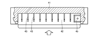
광전 플렉서블 배선판(30)에서 특징적인 것은 광 전송로(33)의 구조이다. 이 광 전송로(33)는 전기 전송로(32) 열(列)의 더욱 외측에 판상 베이스(31)의 전장에 걸쳐 연속적으로 그리고 평행하게 형성되어 있다. 이에 따라, 광전 플렉서블 배선 판(30)으로부터는 광전 변환을 행하는 광 소자 및 그 드라이버가 배제되어 있다. 즉, 광 전송로(33)는 광전 플렉서블 배선판의 일단으로부터 타단까지 연속해서 형성되어 있고, 그 양단의 신호 입출구는 광전 플렉서블 배선판(30)의 양단면에 노출 개구되어 있다.The characteristic of the photoelectric
커넥터(40, 50)는 실질적으로 동일한 구조의 플러그 타입이며, 그 구조를 한쪽의 커넥터(40)에 대해서 도 2∼도 5에 의해 설명한다. 커넥터(40)는 광전 플렉서블 배선판(30)의 횡폭보다 긴 횡폭을 가진 직사각형의 수지 바디(41)를 가지고 있다. 수지 바디(41)의 정면에는 광전 플렉서블 배선판(30)의 단부가 삽입되는 횡으로 긴 가이드 구멍(42)이 형성되어 있다.The
이 수지 바디(41)내에는 광전 플렉서블 배선판(30)에 있어서의 전기 전송로(32)의 개수에 대응하는 개수의 콘택트(43)가 인서트 성형에 의해 형성되어 있다. 복수의 콘택트(43)는 광전 플렉서블 배선판(30)에 있어서의 복수개의 전기 전송로(32)에 각각 대응하고 있고, 전기 전송로(32)와 같은 간격으로 수지 바디(41)중에 형성되어 있다.In this
각 콘택트(43)의 일단부는 광전 플렉서블 배선판(30)의 단부가 가이드 구멍(42)에 삽입되었을 때에 그 상면의 전기 전송로(32)에 압접하는 접촉 단자로서 기능하도록 가이드 구멍(42)의 천정면을 따라 정면측으로 직선상으로 돌출되어 있다. 각 콘택트(42)의 타단부는 실장 기판(12)상으로의 실장 고정 및 실장 기판(12)상의 전기 회로와의 접속을 위한 접속 단자로서, 수지 바디(41)의 후측에 L상으로 돌출되어 있다.One end of each of the
수지 바디(41)내에는 광전 변환을 행하는 광 소자(45)가 광전 플렉서블 배선판(30)의 광 전송로(33)에 대응해서 설치되어 있다. 광 소자(45)는 광 전송로(33)가 광전 플렉서블 배선판의 측연부(側緣部)(전기 전송로 열의 외측)에 있기 때문에 수지 바디(41)의 측단부, 보다 자세하게는 복수의 콘택트(43)의 더욱 외측에 위치하고 있다. 그리고, 광전 플렉서블 배선판(30)의 단부가 가이드 구멍(42)에 삽입되었을 때에 광 전송로(33)의 단면의 신호 입출구에 대향하도록 광 소자(45)는 가이드 구멍(42) 속에 정면을 향해서 배치되어 있다.In the
광 소자(45)의 접속 단자(46)는 실장 기판(12)상으로의 실장 고정 및 실장 기판(12)상의 전기 회로와의 접속 때문에 콘택트(43)의 접속 단자와 같이 수지 바디(41)의 후측에 L상으로 돌출되어 있다.The
커넥터(40)내의 광 소자(45)를 구동하는 드라이버(60)는 커넥터(40)와 함께 실장 기판(12)상에 실장되어 있다.The
뚜껑체(20)내의 커넥터(50)에 대해서도 실장 기판(22)의 단부상에 실장되고, 광전 플렉서블 배선판(30)의 광 전송로(33)에 대응하는 광 소자(55)를 내장하고 있다. 광 소자(55)를 구동하는 드라이버(70)는 커넥터(50)와 함께 실장 기판(22)상에 실장되어 있다.The
본 실시형태에 의한 광전 플렉서블 배선판의 배선 구조에 있어서는 전자 기기의 본체(10)내의 실장 기판(12)과 뚜껑체(20)내의 실장 기판(22)의 사이가 커넥터(40), 광전 플렉서블 배선판(30) 및 커넥터(50)를 통해 전기적 및 광학적으로 접속된다. 즉, 광전 플렉서블 배선판(30)의 일단부를 커넥터(40)에 삽입하고, 타단부 를 커넥터(50)에 삽입함으로써 실장 기판(12, 22)이 광전 플렉서블 배선판(30)에 의해 광전적으로 접속된다.In the wiring structure of the photovoltaic flexible wiring board according to the present embodiment, the
구체적으로 설명하면, 광전 플렉서블 배선판(30)의 일단부를 커넥터(40)의 가이드 구멍(42)에 삽입함으로써 복수개의 콘택트(43)의 각 접촉 단자가 광전 플렉서블 배선판(30)의 표면에 배치된 복수개의 전기 전송로(32)의 대응하는 단부(신호 입출구)에 접촉한다. 그리고, 광전 플렉서블 배선판(30)의 타단부를 커넥터(50)의 가이드 구멍에 삽입함으로써 그 복수개의 콘택트의 각 접촉 단자가 광전 플렉서블 배선판(30)의 표면에 배치된 복수개의 전기 전송로(32)의 대응하는 단부(신호 입출구)에 접촉한다. 이에 따라, 커넥터(40)내의 콘택트(43), 광전 플렉서블 배선판(30)의 전기 전송로(32) 및 콘택트(50)내의 콘택트를 통해 실장 기판(12, 22) 사이에서의 전기 신호의 전송이 행해진다.Specifically, a plurality of contact terminals of the plurality of
광 신호의 전송에 대해서는 광전 플렉서블 배선판(30)의 일단부를 커넥터(40)의 가이드 구멍(42)에 삽입함으로써 광전 플렉서블 배선판(30)의 광 전송로(33)의 단면(신호 입출구)이 커넥터(40)내의 광 소자(45)에 대향한다. 그리고, 광전 플렉서블 배선판(30)의 타단부를 커넥터(50)의 가이드 구멍에 삽입함으로써 광전 플렉서블 배선판(30)의 광 전송로(33)의 단면(신호 입출구)이 커넥터(50)내의 광 소자(55)에 대향한다. 이에 따라, 커넥터(40, 50)내의 광 소자(45, 55)가 광전 플렉서블 배선판(30)의 광 전송로(33)를 통해 접속된다. 이 결과, 다음과 같이 광 신호의 전송이 행해진다.For transmission of the optical signal, one end of the photoelectric
예를 들면, 커넥터(40)내의 광 소자(45)에 의해 전기 신호가 광 신호로 변환 되고, 광전 플렉서블 배선판(30)의 광 전송로(33)를 통과하여 커넥터(50)내의 광 소자(55)로 전송되고, 여기에서 다시 전기 신호로 변화된다. 또는, 커넥터(50)내의 광 소자(55)에 의해 전기 신호가 광 신호로 변환되고, 광전 플렉서블 배선판(30)의 광 전송로(33)를 통과하여 커넥터(40)내의 광 소자(45)로 전송되고, 여기에서 다시 전기 신호로 변화된다.For example, an electrical signal is converted into an optical signal by the
여기에서는 광전 플렉서블 배선판(30)의 광 전송로(33)에 부수되는 광 소자(45, 55) 및 드라이버(60, 70)가 광전 플렉서블 배선판(30)상에 없고, 이것들은 실장 기판(12, 22)상에 탑재되어 있다. 이로 인해, 광전 플렉서블 배선판(30)의 단부로부터 단부까지, 즉 전장이 굴곡 가능한 광 전송 구간이 되고, 광 소자(45. 55) 등에 의해 이것이 저해되는 경우에 비해 굴곡성이 향상된다. 즉, 광전 플렉서블 배선판(30)의 길이가 같다고 하면 굴곡성이 향상되고, 같은 굴곡성을 확보할 경우는 광전 플렉서블 배선판(30)의 길이를 단축할 수 있다.Here, the
광전 플렉서블 배선판(30)상에 광 소자(45, 55) 및 드라이버(60, 70)를 실장하지 않음으로써 광전 플렉서블 배선판(30)에 있어서의 실장 가격을 저감할 수 있고, 광전 플렉서블 배선판(30)의 경제성을 높일 수 있다.By not mounting the
또한, 광전 플렉서블 배선판(30)상에서 광 전기 변환이 행해지지 않게 되기 때문에 광전 플렉서블 배선판(30)에서의 광 전송 특성의 저하가 저지되어 EMC 대책, 신호 열화 대책상 대단히 유리하게 된다.In addition, since the photoelectric conversion is not performed on the photoelectric
도 6은 본 발명의 다른 실시형태를 나타내는 커넥터의 사시도, 도 7은 동 커넥터의 횡단 평면도로서 도 6 중의 B-B선 단면도이다.6 is a perspective view of a connector showing another embodiment of the present invention, and FIG. 7 is a cross-sectional view taken along line B-B in FIG. 6 as a cross-sectional plan view of the connector.
본 실시형태는 도 1∼도 5에 도시된 실시형태에 비해 커넥터(40)에 있어서의 광 소자(45)의 위치가 상위하다. 즉, 도 1∼도 5에 도시된 실시형태에서는 광 소자(45)가 가이드 구멍(42)의 이면, 즉 삽입된 광전 플렉서블 배선판(30)의 단면이 대향하는 위치에 있었지만, 본 실시형태에서는 광 소자(45)가 가이드 구멍(42)에 삽입된 광전 플렉서블 배선판(30)의 단부 상면에 대향하는 위치에 있고, 광전 플렉서블 배선판(30)의 광 전송로(33)에 대하여 수직으로 배치되어 있는 것이다. 이에 따라, 광전 플렉서블 배선판(30)의 광 전송로(33)의 양단부에 있어서는 해당 배선판(30)내의 광 도파로를 직각으로 절곡하는 도파로 미러가 설치되어 있고, 신호 입출구가 해당 배선판(30)의 표면에 개구되어 있다.In this embodiment, the position of the
광 소자(45)의 접속 단자(46)는 실장 기판(12)상으로의 실장 고정 및 실장 기판(12)상의 전기 회로와의 접속 때문에 콘택트(43)의 접속 단자와 마찬가지로 수지 바디(41)의 후측에 L상으로 돌출되어 있다.The
도 8은 본 발명의 또 다른 실시형태를 나타내는 광전 플렉서블 배선판의 배선 구조의 개략 구성도이며 측면도, 도 9는 동 배선 구조의 평면도, 도 10은 동 배선 구조의 횡단 평면도로서 도 8 중의 C-C선 단면도, 도 11 및 도 12는 동 배선 구조에 있어서의 광전 플렉서블 배선판 및 커넥터의 관계를 나타내는 종단 측면도이다.8 is a schematic configuration diagram of a wiring structure of a photoelectric flexible wiring board according to still another embodiment of the present invention. FIG. 9 is a plan view of the wiring structure of FIG. 9, and FIG. 10 is a cross-sectional plan view of the wiring structure of FIG. 8. 11 and 12 are longitudinal side views illustrating the relationship between the photoelectric flexible wiring board and the connector in the wiring structure.
본 실시형태에 있어서는, 도 6 및 도 7에 도시된 실시형태와 마찬가지로, 커넥터(40)에 있어서의 광 소자(45)가 광전 플렉서블 배선판(30)의 광 전송로(33)에 대하여 수직이 되도록 배치되어 있고, 보다 구체적으로는 가이드 구멍(42)에 삽입 된 광전 플렉서블 배선판(30)의 단부 상면에 대향하도록 가이드 구멍(42)의 천정면에 하향으로 배치되어 있다. 광 소자(45)의 리드부는 수지 바디(41)내에 매설되어 있고, 그 선단부는 실장 기판(12)상으로의 실장 고정 및 실장 기판(12)상의 전기 회로와의 접속을 위한 접속 단자(46)로서, 콘택트(43)의 접속 단자와 마찬가지로 수지 바디(41)의 하단부 후면으로부터 실장 기판(12)을 따라 돌출되어 있다. 또한, 커넥터(50)도 커넥터(40)와 마찬가지의 구성으로 되어 있다.In the present embodiment, similarly to the embodiment shown in FIGS. 6 and 7, the
광전 플렉서블 배선판(30)은 플렉서블한 판상 베이스(31)를 구비하고 있다. 판상 베이스(31)의 표면, 보다 구체적으로는 표면의 일측부를 제외한 부분에는 복수개의 전기 전송로(32)가 전장에 걸쳐 병렬상으로 프린팅되어 있다. 판상 베이스(31)의 일측부에는 복수개의 광 전송로(33)가 일단부로부터 타단부에 걸쳐서 병렬로 매설되어 있다. 각 광 전송로(33)의 양단부에서는 광 전송로(33)에 있어서의 광 도파로를 상방으로 직각으로 절곡하는 도파로 미러(35)가 설치되어 있고, 신호 입출구(36)가 판상 베이스(31)의 상표면에 개구되어 있다. 이에 따라, 광전 플렉서블 배선판(30)의 양단부를 커넥터(40)의 가이드 구멍(42), 커넥터(50)의 가이드 구멍에 각각 삽입했을 때에 각 광 전송로(33)의 신호 입출구(36)가 광 소자(45, 55)와 대향한다.The photoelectric
광전 플렉서블 배선판(30)의 양단부에는 또한, 오목 형상의 고정부(39, 39)가 양쪽 에지부에 위치해서 형성되어 있다. 오목 형상의 고정부(39, 39)는 광전 플렉서블 배선판(30)의 양단부를 커넥터(40)의 가이드 구멍(42), 커넥터(50)의 가이드 구멍에 각각 삽입한 상태에서 커넥터(40)의 가이드 구멍(42)내에 돌출된 양측의 볼록부(49, 49), 커넥터(50)의 가이드 구멍내에 돌출된 양측의 볼록부(59, 59)와 감합하고, 이 감합에 의해 광전 플렉서블 배선판(30)의 삽입 단부를 유지한다.On both ends of the photoelectric
도 13은 본 발명의 또 다른 실시형태를 나타내는 광전 플렉서블 배선판의 주요부의 종단 측면도이다.It is a longitudinal side view of the principal part of the photoelectric flexible wiring board which shows another embodiment of this invention.
본 실시형태는 도 8∼도 12에 도시된 실시형태에 비해 광전 플렉서블 배선판(30)이 상위하다. 본 실시형태에서의 광전 플렉서블 배선판(30)은, 도 1∼도 5에 도시된 실시형태와 마찬가지로, 판상 베이스(31) 중의 광 전송로(33)가 그 베이스의 일단으로부터 타단으로 전장에 걸쳐 배치되어 있고, 양단의 신호 입출구(36)는 판상 베이스(31)의 양단면에 길이 방향으로 개구되어 있다. 커넥터(40, 50)에 있어서의 광 소자(45, 55)에 대해서도, 도 1∼도 5에 도시된 실시형태와 마찬가지로, 광전 플렉서블 배선판(30)의 양단부가 커넥터(40, 50)의 가이드 구멍에 삽입된 상태에서 양단의 신호 입출구(36)에 직접 마주보도록 가이드 구멍의 이면에 부착되어 있다. 다른 구조는 도 8∼도 12에 도시된 실시형태와 마찬가지이다.In this embodiment, the photoelectric
본 실시형태에서도 광전 플렉서블 배선판(30)의 전장에 걸쳐 광 전송로(33)가 형성되어 있다. 즉, 광전 플렉서블 배선판(30)의 커넥터(40, 50)에 삽입되는 양단부 사이에 광 전송로(33)가 배치되어 있고, 광전 플렉서블 배선판(30)상으로부터 광 소자(45, 55) 및 드라이버(60, 70)가 배제되어 있다. 이로 인해, 광전 플렉서블 배선판(30)에 있어서의 실장 가격을 저감할 수 있고, 광전 플렉서블 배선판(30)의 경제성을 높일 수 있다. 또한, 광전 플렉서블 배선판(30)상에서 광 전기 변환이 행해지지 않게 되기 때문에 광전 플렉서블 배선판(30)에서의 광 전송 특성의 저하가 저지되어, EMC 대책, 신호 열화 대책상 대단히 유리하게 된다.Also in this embodiment, the
이것들의 실시형태로부터 알 수 있는 바와 같이, 커넥터(40, 50)에 있어서의 광 소자(45, 55)는 광전 플렉서블 배선판(30)의 광 전송로(33)의 양단부 단면에 정대하는 방향으로 배치해도 좋고, 광 전송로(33)에 직각 방향으로부터 대향하는 방향으로 배치해도 좋고, 특히 그 방향을 한정하는 것은 아니다. 이에 따라, 광전 플렉서블 배선판(30)의 광 전송로(33)의 단부(신호 입출구)는 광 소자(45. 55)에 대향하도록 이것들의 방향에 따라서 그 방향이 결정된다.As can be seen from these embodiments, the
광전 플렉서블 배선판(30)의 광 전송로(33)는 또한, 상술한 실시형태에서는 전기 전송로(32)의 열의 외측, 배선판의 한쪽의 측연부에 일렬 또는 복수열로 배치되어 있고, 이에 따라 광 소자(45)는 커넥터(40)의 측단부에 설치되어 있지만, 이 위치에 한정되는 것은 아니고, 전기 전송로(32)의 열의 양측에 배치해도 좋고, 전송로(32)에 끼워진 위치에 배치해도 좋다. 전기 전송로(32)의 열의 외측에 광 전송로(33)를 배치하고, 이에 따라 광 소자(45)를 커넥터(40)의 측단부에 설치한 경우는 실장 기판(12)상에 있어서의 드라이버(60)의 배치 스페이스의 확보가 용이해지는 것은 전술한 바와 같다.In the above-described embodiment, the
커넥터(40, 50)에 삽입된 광전 플렉서블 배선판(30)의 고정에 대해서는 상술한 실시형태에서는 요철 감합을 설명했지만, 커넥터(40, 50)의 가이드 구멍에 광전 플렉서블 배선판(30)을 삽입한 후, 더욱 슬라이더를 직선적으로 삽입하는 구조를 채용해도 좋다. 이외에도, 커넥터(40, 50)의 가이드 구멍에 슬라이더를 회동에 의해 삽입하는 고정 구조를 채용할 수도 있고, 그 이외에도 여러가지 고정 구조를 채 용할 수 있다. 삽입된 광전 플렉서블 배선판(30)을 확실하게 고정할 수 있을수록 광 소자(45, 55)와 광 전송로(33)의 위치 맞춤은 확실하고 용이하게 된다.For the fixing of the photoelectric
Claims (11)
Applications Claiming Priority (5)
| Application Number | Priority Date | Filing Date | Title |
|---|---|---|---|
| JP2006027689 | 2006-02-03 | ||
| JPJP-P-2006-00027689 | 2006-02-03 | ||
| JPJP-P-2006-00165020 | 2006-06-14 | ||
| JP2006165020A JP4711895B2 (en) | 2006-02-03 | 2006-06-14 | Photoelectric flexible wiring board connection structure, connector and photoelectric flexible wiring board |
| PCT/JP2007/051369 WO2007088805A1 (en) | 2006-02-03 | 2007-01-29 | Connection structure of photoelectric flexible wiring board, connector and photoelectric flexible wiring board |
Publications (2)
| Publication Number | Publication Date |
|---|---|
| KR20080098008A true KR20080098008A (en) | 2008-11-06 |
| KR101274547B1 KR101274547B1 (en) | 2013-06-13 |
Family
ID=38327380
Family Applications (1)
| Application Number | Title | Priority Date | Filing Date |
|---|---|---|---|
| KR1020087018239A Expired - Fee Related KR101274547B1 (en) | 2006-02-03 | 2007-01-29 | Connection structure of photoelectric flexible wiring board, connector and photoelectric flexible wiring board |
Country Status (7)
| Country | Link |
|---|---|
| US (1) | US7780359B2 (en) |
| EP (1) | EP1986278B1 (en) |
| JP (1) | JP4711895B2 (en) |
| KR (1) | KR101274547B1 (en) |
| CN (1) | CN101379662B (en) |
| TW (1) | TWI390740B (en) |
| WO (1) | WO2007088805A1 (en) |
Families Citing this family (20)
| Publication number | Priority date | Publication date | Assignee | Title |
|---|---|---|---|---|
| US7684663B2 (en) * | 2007-11-02 | 2010-03-23 | National Semiconductor Corporation | Coupling of optical interconnect with electrical device |
| US7627204B1 (en) * | 2007-11-02 | 2009-12-01 | National Semiconductor Corporation | Optical-electrical flex interconnect using a flexible waveguide and flexible printed circuit board substrate |
| JP5211940B2 (en) * | 2008-08-29 | 2013-06-12 | 日立化成株式会社 | Optical waveguide, opto-electric hybrid board and optical module |
| KR101023137B1 (en) * | 2008-10-27 | 2011-03-23 | 한국광기술원 | Photoelectric wiring board connector using photoelectric mixed connector |
| WO2010050919A1 (en) | 2008-10-31 | 2010-05-06 | Hewlett-Packard Development Company, L.P. | Variably configurable computer buses |
| WO2010058476A1 (en) | 2008-11-21 | 2010-05-27 | 日立化成工業株式会社 | Photoelectric hybrid board and electronic apparatus |
| JP5386999B2 (en) * | 2009-01-15 | 2014-01-15 | 日立化成株式会社 | Optical module and electrical connection method |
| JP4920723B2 (en) * | 2009-05-14 | 2012-04-18 | シャープ株式会社 | Transmission system for image display device and electronic device |
| JP2011095333A (en) * | 2009-10-27 | 2011-05-12 | Toshiba Corp | Mounting structure |
| US8620122B2 (en) * | 2010-09-10 | 2013-12-31 | Avago Technologies General Ip (Singapore) Pte. Ltd. | Low-profile optical communications module having two generally flat optical connector modules that slidingly engage one another |
| CN103189775A (en) | 2010-11-05 | 2013-07-03 | 株式会社村田制作所 | Connector |
| KR101266616B1 (en) * | 2011-11-29 | 2013-05-22 | 엘에스엠트론 주식회사 | Optical interconnection module |
| CN103428997A (en) * | 2012-05-23 | 2013-12-04 | 鸿富锦精密工业(深圳)有限公司 | Photoelectric circuit board and circuit board module |
| JP2016143018A (en) * | 2015-02-05 | 2016-08-08 | ソニー株式会社 | Optical transmitter, optical receiver and optical fiber |
| DE112015006664T5 (en) * | 2015-07-01 | 2018-05-24 | Intel Corporation | FPC connectors for better signal integrity and design compaction |
| KR101924939B1 (en) * | 2017-02-24 | 2018-12-04 | 주식회사 지파랑 | Slim Type Connector Plug, Active Optical Cable Assembly Using the Same and Method of Manufacturing the Same |
| US12429658B2 (en) | 2017-02-24 | 2025-09-30 | Lipac Co., Ltd. | Optical element module, slim connector plug, active optical cable assembly using same, and manufacturing method thereof |
| JP6661733B1 (en) * | 2018-11-28 | 2020-03-11 | 株式会社フジクラ | Cable and image transmission system |
| DE102019003842A1 (en) * | 2019-06-03 | 2020-12-03 | Karl Storz Se & Co. Kg | Endoscope and method for producing an endoscope |
| JP7137274B2 (en) * | 2019-08-02 | 2022-09-14 | ヒロセ電機株式会社 | Connector assembly arrangement structure |
Family Cites Families (21)
| Publication number | Priority date | Publication date | Assignee | Title |
|---|---|---|---|---|
| US4678264A (en) * | 1983-03-30 | 1987-07-07 | Amp Incorporated | Electrical and fiber optic connector assembly |
| US5125054A (en) * | 1991-07-25 | 1992-06-23 | Motorola, Inc. | Laminated polymer optical waveguide interface and method of making same |
| US5396573A (en) * | 1993-08-03 | 1995-03-07 | International Business Machines Corporation | Pluggable connectors for connecting large numbers of electrical and/or optical cables to a module through a seal |
| JP3705873B2 (en) * | 1996-10-17 | 2005-10-12 | 株式会社アドバンテスト | Optical / electric mixed wiring board |
| JP2001507814A (en) * | 1996-12-31 | 2001-06-12 | ハネウエル・インコーポレーテッド | Flexible optical connector assembly |
| US6690845B1 (en) * | 1998-10-09 | 2004-02-10 | Fujitsu Limited | Three-dimensional opto-electronic modules with electrical and optical interconnections and methods for making |
| JP4164947B2 (en) * | 1999-06-25 | 2008-10-15 | 凸版印刷株式会社 | Optical / electrical wiring board, manufacturing method, and mounting board |
| JP2001042171A (en) * | 1999-07-28 | 2001-02-16 | Canon Inc | Active optical wiring equipment |
| JP3331409B2 (en) * | 1999-08-02 | 2002-10-07 | 日本航空電子工業株式会社 | Photoelectric composite connector |
| JP2001311846A (en) * | 2000-04-28 | 2001-11-09 | Oki Printed Circuit Kk | Method for manufacturing electric wiring/optical wiring coexisting multilayer sheet and method for manufacturing electric wiring/optical wiring coexisting multilayer substrate |
| US7101091B2 (en) * | 2001-02-21 | 2006-09-05 | Zarlink Semiconductor, Inc. | Apparatus for coupling a fiber optic cable to an optoelectronic device, a system including the apparatus, and a method of forming the same |
| JP2003227951A (en) * | 2002-02-05 | 2003-08-15 | Canon Inc | Optical waveguide device, manufacturing method thereof, and opto-electric hybrid board using the same |
| EP1286194A3 (en) * | 2001-08-21 | 2004-05-19 | Canon Kabushiki Kaisha | Optical waveguide apparatus |
| US6882762B2 (en) * | 2001-09-27 | 2005-04-19 | Intel Corporation | Waveguide in a printed circuit board and method of forming the same |
| US7156690B2 (en) * | 2002-01-07 | 2007-01-02 | Bernard R Tolmie | Extruded connector without channel insulating layer |
| KR100730320B1 (en) * | 2002-05-28 | 2007-06-19 | 마츠시다 덴코 가부시키가이샤 | Material for substrate mounting optical circuit-electric circuit mixedly and substrate mounting optical circuit-electric circuit mixedly |
| JP2004031508A (en) | 2002-06-24 | 2004-01-29 | Nec Corp | Photoelectric composite module and optical input / output device comprising the module as a component |
| JP2004191564A (en) * | 2002-12-10 | 2004-07-08 | Mitsubishi Electric Corp | Optical path conversion connector |
| JP2005300930A (en) | 2004-04-12 | 2005-10-27 | Matsushita Electric Works Ltd | Method for manufacturing optical and electrical consolidated substrate |
| US7458732B2 (en) * | 2004-12-22 | 2008-12-02 | Panasonic Electric Works Co., Ltd. | Optical and electrical compound connector |
| JP2007033688A (en) * | 2005-07-25 | 2007-02-08 | Fuji Xerox Co Ltd | Optical waveguide film and optical transmission and reception module |
-
2006
- 2006-06-14 JP JP2006165020A patent/JP4711895B2/en active Active
-
2007
- 2007-01-18 TW TW096101939A patent/TWI390740B/en not_active IP Right Cessation
- 2007-01-29 US US12/162,870 patent/US7780359B2/en active Active
- 2007-01-29 CN CN2007800043715A patent/CN101379662B/en not_active Expired - Fee Related
- 2007-01-29 WO PCT/JP2007/051369 patent/WO2007088805A1/en not_active Ceased
- 2007-01-29 EP EP07707600.8A patent/EP1986278B1/en not_active Ceased
- 2007-01-29 KR KR1020087018239A patent/KR101274547B1/en not_active Expired - Fee Related
Also Published As
| Publication number | Publication date |
|---|---|
| EP1986278A1 (en) | 2008-10-29 |
| EP1986278A4 (en) | 2012-04-11 |
| US7780359B2 (en) | 2010-08-24 |
| TW200735384A (en) | 2007-09-16 |
| EP1986278B1 (en) | 2016-11-16 |
| JP2007233325A (en) | 2007-09-13 |
| WO2007088805A1 (en) | 2007-08-09 |
| CN101379662A (en) | 2009-03-04 |
| KR101274547B1 (en) | 2013-06-13 |
| TWI390740B (en) | 2013-03-21 |
| US20090041408A1 (en) | 2009-02-12 |
| CN101379662B (en) | 2011-12-14 |
| JP4711895B2 (en) | 2011-06-29 |
Similar Documents
| Publication | Publication Date | Title |
|---|---|---|
| KR101274547B1 (en) | Connection structure of photoelectric flexible wiring board, connector and photoelectric flexible wiring board | |
| US7645075B2 (en) | Optical connection structure of optical backplane to circuit substrate | |
| CN101060549B (en) | Portable telephone and electronic equipment | |
| US8322933B2 (en) | Optical connection structure between optical backplane and circuit substrate | |
| JP4238187B2 (en) | Photoelectric composite connector and board using the same | |
| CN1761107B (en) | Photoelectric composite wiring part and electronic equipment using the same | |
| KR20040034387A (en) | Optical backplane array connector | |
| US9417414B2 (en) | Optical connector for a card including concave and convex guide portions | |
| US9379467B2 (en) | Optical connector having a press-fit guide portion | |
| US7396166B1 (en) | Optical transceiver module | |
| WO2009045366A1 (en) | Flat opto-electric hybrid connector system | |
| JP5445026B2 (en) | Electric light composite harness | |
| CN115207723A (en) | Connector and communication equipment | |
| CN101191874B (en) | Optical transmission device and electronic equipment with use thereof | |
| KR100798012B1 (en) | Data link module | |
| JP4344328B2 (en) | Photoelectric composite connector | |
| CN121399519A (en) | Optoelectronic module | |
| CN121399520A (en) | Optoelectronic module | |
| KR200394725Y1 (en) | Mounting structure of printed circuit board of input/output plug for cradle |
Legal Events
| Date | Code | Title | Description |
|---|---|---|---|
| E13-X000 | Pre-grant limitation requested |
St.27 status event code: A-2-3-E10-E13-lim-X000 |
|
| PA0105 | International application |
St.27 status event code: A-0-1-A10-A15-nap-PA0105 |
|
| PG1501 | Laying open of application |
St.27 status event code: A-1-1-Q10-Q12-nap-PG1501 |
|
| PN2301 | Change of applicant |
St.27 status event code: A-3-3-R10-R13-asn-PN2301 St.27 status event code: A-3-3-R10-R11-asn-PN2301 |
|
| A201 | Request for examination | ||
| PA0201 | Request for examination |
St.27 status event code: A-1-2-D10-D11-exm-PA0201 |
|
| E902 | Notification of reason for refusal | ||
| PE0902 | Notice of grounds for rejection |
St.27 status event code: A-1-2-D10-D21-exm-PE0902 |
|
| P11-X000 | Amendment of application requested |
St.27 status event code: A-2-2-P10-P11-nap-X000 |
|
| P13-X000 | Application amended |
St.27 status event code: A-2-2-P10-P13-nap-X000 |
|
| E701 | Decision to grant or registration of patent right | ||
| PE0701 | Decision of registration |
St.27 status event code: A-1-2-D10-D22-exm-PE0701 |
|
| GRNT | Written decision to grant | ||
| PR0701 | Registration of establishment |
St.27 status event code: A-2-4-F10-F11-exm-PR0701 |
|
| PR1002 | Payment of registration fee |
St.27 status event code: A-2-2-U10-U12-oth-PR1002 Fee payment year number: 1 |
|
| PG1601 | Publication of registration |
St.27 status event code: A-4-4-Q10-Q13-nap-PG1601 |
|
| FPAY | Annual fee payment |
Payment date: 20160517 Year of fee payment: 4 |
|
| PR1001 | Payment of annual fee |
St.27 status event code: A-4-4-U10-U11-oth-PR1001 Fee payment year number: 4 |
|
| FPAY | Annual fee payment |
Payment date: 20170522 Year of fee payment: 5 |
|
| PR1001 | Payment of annual fee |
St.27 status event code: A-4-4-U10-U11-oth-PR1001 Fee payment year number: 5 |
|
| FPAY | Annual fee payment |
Payment date: 20180516 Year of fee payment: 6 |
|
| PR1001 | Payment of annual fee |
St.27 status event code: A-4-4-U10-U11-oth-PR1001 Fee payment year number: 6 |
|
| FPAY | Annual fee payment |
Payment date: 20190515 Year of fee payment: 7 |
|
| PR1001 | Payment of annual fee |
St.27 status event code: A-4-4-U10-U11-oth-PR1001 Fee payment year number: 7 |
|
| PR1001 | Payment of annual fee |
St.27 status event code: A-4-4-U10-U11-oth-PR1001 Fee payment year number: 8 |
|
| PR1001 | Payment of annual fee |
St.27 status event code: A-4-4-U10-U11-oth-PR1001 Fee payment year number: 9 |
|
| PR1001 | Payment of annual fee |
St.27 status event code: A-4-4-U10-U11-oth-PR1001 Fee payment year number: 10 |
|
| PC1903 | Unpaid annual fee |
St.27 status event code: A-4-4-U10-U13-oth-PC1903 Not in force date: 20230608 Payment event data comment text: Termination Category : DEFAULT_OF_REGISTRATION_FEE |
|
| PC1903 | Unpaid annual fee |
St.27 status event code: N-4-6-H10-H13-oth-PC1903 Ip right cessation event data comment text: Termination Category : DEFAULT_OF_REGISTRATION_FEE Not in force date: 20230608 |