JP4704322B2 - 光電気混載基板の製造方法 - Google Patents
光電気混載基板の製造方法 Download PDFInfo
- Publication number
- JP4704322B2 JP4704322B2 JP2006324310A JP2006324310A JP4704322B2 JP 4704322 B2 JP4704322 B2 JP 4704322B2 JP 2006324310 A JP2006324310 A JP 2006324310A JP 2006324310 A JP2006324310 A JP 2006324310A JP 4704322 B2 JP4704322 B2 JP 4704322B2
- Authority
- JP
- Japan
- Prior art keywords
- insulating member
- member forming
- mirror
- forming mold
- wiring board
- Prior art date
- Legal status (The legal status is an assumption and is not a legal conclusion. Google has not performed a legal analysis and makes no representation as to the accuracy of the status listed.)
- Active
Links
Images


Classifications
-
- G—PHYSICS
- G02—OPTICS
- G02B—OPTICAL ELEMENTS, SYSTEMS OR APPARATUS
- G02B6/00—Light guides; Structural details of arrangements comprising light guides and other optical elements, e.g. couplings
- G02B6/10—Light guides; Structural details of arrangements comprising light guides and other optical elements, e.g. couplings of the optical waveguide type
- G02B6/12—Light guides; Structural details of arrangements comprising light guides and other optical elements, e.g. couplings of the optical waveguide type of the integrated circuit kind
-
- G—PHYSICS
- G02—OPTICS
- G02B—OPTICAL ELEMENTS, SYSTEMS OR APPARATUS
- G02B6/00—Light guides; Structural details of arrangements comprising light guides and other optical elements, e.g. couplings
- G02B6/24—Coupling light guides
- G02B6/42—Coupling light guides with opto-electronic elements
- G02B6/43—Arrangements comprising a plurality of opto-electronic elements and associated optical interconnections
-
- G—PHYSICS
- G02—OPTICS
- G02B—OPTICAL ELEMENTS, SYSTEMS OR APPARATUS
- G02B6/00—Light guides; Structural details of arrangements comprising light guides and other optical elements, e.g. couplings
- G02B6/24—Coupling light guides
- G02B6/42—Coupling light guides with opto-electronic elements
- G02B6/4201—Packages, e.g. shape, construction, internal or external details
- G02B6/4204—Packages, e.g. shape, construction, internal or external details the coupling comprising intermediate optical elements, e.g. lenses, holograms
- G02B6/4214—Packages, e.g. shape, construction, internal or external details the coupling comprising intermediate optical elements, e.g. lenses, holograms the intermediate optical element having redirecting reflective means, e.g. mirrors, prisms for deflecting the radiation from horizontal to down- or upward direction toward a device
-
- H—ELECTRICITY
- H05—ELECTRIC TECHNIQUES NOT OTHERWISE PROVIDED FOR
- H05K—PRINTED CIRCUITS; CASINGS OR CONSTRUCTIONAL DETAILS OF ELECTRIC APPARATUS; MANUFACTURE OF ASSEMBLAGES OF ELECTRICAL COMPONENTS
- H05K1/00—Printed circuits
- H05K1/02—Details
- H05K1/0274—Optical details, e.g. printed circuits comprising integral optical means
Description
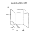
図6は、本発明の第1の実施の形態に係る光電気混載基板の断面図である。
図20は、本発明の第2の実施の形態に係る光電気混載基板の断面図である。図20において、第1の実施の形態の光電気混載基板10と同一構成部分には同一符号を付す。
図21は、本発明の第3の実施の形態に係る光電気混載基板の断面図である。図21において、第1の実施の形態の光電気混載基板10と同一構成部分には同一符号を付す。
図22は、本発明の第4の実施の形態に係る光電気混載基板の断面図である。図22において、第3の実施の形態の光電気混載基板110と同一構成部分には同一符号を付す。
図23は、本発明の第5の実施の形態に係る光電気混載基板の断面図である。図23において、第1の実施の形態の光電気混載基板と同一構成部分には同一符号を付す。
11,101,131 配線基板
12,13,132,133 絶縁部材
12A,13A,83A,84A,132A,133A,145B,146B 傾斜面
14,15,134,135 ミラー
17,111 光導波路
17A 端面
21 発光素子
22 受光素子
24 はんだ
25,26 アンダーフィル樹脂
31 コア基板
31A,41A,57A,114A 上面
31B,42A 下面
32,33 貫通ビア
35,36,38,39 配線
41,42 絶縁層
44,45,47,48 ビア
51,52,54,55 配線パターン
51A,52A,53A,54A 接続部
57,58 ソルダーレジスト
57D,57E 面
61,62 貫通孔
57A,57B,58A,58B,64〜67,137,153A,153B 開口部
71,112 第1クラッド層
72,106,113 コア部
73,114 第2クラッド層
74,104 接着剤
76,78 バンプ
77 発光部
79 受光部
81,82,145,146 絶縁部材形成用型体
81A,82A,132B,133B,145A,146A 底面
83,84 溝部
86,151 紫外線硬化樹脂
88,153 レジスト膜
91,155 金属膜
103 光ファイバ
107 クラッド層
138,139 段差部
145C,146C 側面
147,148 切り欠き部
B,C 空間
θ1〜θ10 傾斜角度
Claims (2)
- 配線基板と、前記配線基板上に設けられ、光信号の伝送を行う光導波路と、前記光信号を反射させるミラーと、を備えた光電気混載基板の製造方法であって、
前記配線基板上に平滑な傾斜面を有した絶縁部材を形成する絶縁部材形成工程と、
前記平滑な傾斜面に前記ミラーを形成するミラー形成工程と、
前記絶縁部材とは別体とされた前記光導波路を準備する光導波路準備工程と、
前記ミラー形成工程後に、前記配線基板上に前記光導波路を接着する光導波路接着工程と、を有し、
前記絶縁部材形成工程は、前記絶縁部材の形状に対応する溝部を有すると共に、紫外線を透過させる絶縁部材形成用型体を準備する絶縁部材形成用型体準備工程と、
前記溝部と前記配線基板とが対向するように絶縁部材形成用型体を前記配線基板に押し当てた後、前記溝部に液状の紫外線硬化樹脂を充填する液状樹脂充填工程と、
前記配線基板に押し当てられた前記絶縁部材形成用型体を介して、前記液状の紫外線硬化樹脂に紫外線を照射して、前記液状の紫外線硬化樹脂を硬化させる樹脂硬化工程と、
前記配線基板から前記絶縁部材形成用型体を取り外す絶縁部材形成用型体取外工程と、を含み、
前記溝部に対応する部分の前記絶縁部材形成用型体の面は、平滑な面であることを特徴とする光電気混載基板の製造方法。 - 配線基板と、前記配線基板上に設けられ、光信号の伝送を行う光導波路と、前記光信号を反射させるミラーと、を備えた光電気混載基板の製造方法であって、
前記配線基板は、前記ミラーの形成領域に対応する部分に段差部を有しており、
前記配線基板上に平滑な傾斜面を有した絶縁部材を形成する絶縁部材形成工程と、
前記平滑な傾斜面に前記ミラーを形成するミラー形成工程と、
前記絶縁部材とは別体とされた前記光導波路を準備する光導波路準備工程と、
前記ミラー形成工程後に、前記配線基板上に前記光導波路を接着する光導波路接着工程と、を有し、
前記絶縁部材形成工程は、前記絶縁部材の形状に対応する切り欠き部を有すると共に、紫外線を透過させる絶縁部材形成用型体を準備する絶縁部材形成用型体準備工程と、
前記切り欠き部が形成された部分の前記絶縁部材形成用型体と前記配線基板の前記段差部とが対向するように、前記絶縁部材形成用型体を前記配線基板に押し当てた後、前記絶縁部材形成用型体と前記段差部とにより形成される空間に液状の紫外線硬化樹脂を充填する液状樹脂充填工程と、
前記配線基板に押し当てられた前記絶縁部材形成用型体を介して、前記液状の紫外線硬化樹脂に紫外線を照射して、前記液状の紫外線硬化樹脂を硬化させる樹脂硬化工程と、
前記配線基板から前記絶縁部材形成用型体を取り外す絶縁部材形成用型体取外工程と、を含み、
前記切り欠き部に対応する部分の前記絶縁部材形成用型体の面は、平滑な面であることを特徴とする光電気混載基板の製造方法。
Priority Applications (3)
| Application Number | Priority Date | Filing Date | Title |
|---|---|---|---|
| JP2006324310A JP4704322B2 (ja) | 2006-11-30 | 2006-11-30 | 光電気混載基板の製造方法 |
| US11/987,064 US7627210B2 (en) | 2006-11-30 | 2007-11-27 | Manufacturing method of optical-electrical substrate and optical-electrical substrate |
| KR1020070122574A KR20080049655A (ko) | 2006-11-30 | 2007-11-29 | 광전기 기판의 제조 방법 및 광전기 기판 |
Applications Claiming Priority (1)
| Application Number | Priority Date | Filing Date | Title |
|---|---|---|---|
| JP2006324310A JP4704322B2 (ja) | 2006-11-30 | 2006-11-30 | 光電気混載基板の製造方法 |
Publications (3)
| Publication Number | Publication Date |
|---|---|
| JP2008139465A JP2008139465A (ja) | 2008-06-19 |
| JP2008139465A5 JP2008139465A5 (ja) | 2009-10-22 |
| JP4704322B2 true JP4704322B2 (ja) | 2011-06-15 |
Family
ID=39475853
Family Applications (1)
| Application Number | Title | Priority Date | Filing Date |
|---|---|---|---|
| JP2006324310A Active JP4704322B2 (ja) | 2006-11-30 | 2006-11-30 | 光電気混載基板の製造方法 |
Country Status (3)
| Country | Link |
|---|---|
| US (1) | US7627210B2 (ja) |
| JP (1) | JP4704322B2 (ja) |
| KR (1) | KR20080049655A (ja) |
Families Citing this family (14)
| Publication number | Priority date | Publication date | Assignee | Title |
|---|---|---|---|---|
| JP4974917B2 (ja) * | 2008-01-29 | 2012-07-11 | 新光電気工業株式会社 | 光導波路の製造方法 |
| JP5399671B2 (ja) * | 2008-09-19 | 2014-01-29 | パナソニック株式会社 | 光電複合基板及びその製造方法 |
| JPWO2010038871A1 (ja) | 2008-10-03 | 2012-03-01 | ソニー株式会社 | 半導体装置 |
| JP5313849B2 (ja) * | 2009-11-30 | 2013-10-09 | 新光電気工業株式会社 | 光導波路装置及びその製造方法 |
| JP5302177B2 (ja) * | 2009-12-18 | 2013-10-02 | 新光電気工業株式会社 | 光導波路基板および光電気混載装置 |
| JP2012088634A (ja) * | 2010-10-22 | 2012-05-10 | Ngk Spark Plug Co Ltd | 光導波路デバイス及びその製造方法 |
| JP5838881B2 (ja) * | 2012-03-27 | 2016-01-06 | 富士通株式会社 | 光射出部材の実装方法及び実装装置 |
| JP6137777B2 (ja) * | 2012-04-17 | 2017-05-31 | インターナショナル・ビジネス・マシーンズ・コーポレーションInternational Business Machines Corporation | 半導体上の発光素子または受光素子と光導波路との間の光の接続損失を低減させることに役立つ、スペーサ樹脂パターンの設計 |
| US9099623B2 (en) | 2013-08-30 | 2015-08-04 | Taiwan Semiconductor Manufacturing Company, Ltd. | Manufacture including substrate and package structure of optical chip |
| US9721812B2 (en) * | 2015-11-20 | 2017-08-01 | International Business Machines Corporation | Optical device with precoated underfill |
| US10025044B1 (en) * | 2017-01-17 | 2018-07-17 | International Business Machines Corporation | Optical structure |
| JP7118731B2 (ja) * | 2018-05-18 | 2022-08-16 | 新光電気工業株式会社 | 光導波路搭載基板、光送受信装置 |
| CN108983374B (zh) * | 2018-08-08 | 2020-04-14 | 华进半导体封装先导技术研发中心有限公司 | 一种光模块封装结构及制作方法 |
| WO2024029011A1 (ja) * | 2022-08-03 | 2024-02-08 | 日本電信電話株式会社 | 光変調器 |
Citations (2)
| Publication number | Priority date | Publication date | Assignee | Title |
|---|---|---|---|---|
| JP2004258065A (ja) * | 2003-02-24 | 2004-09-16 | Ngk Spark Plug Co Ltd | 光導波路基板及びその製造方法、光電気複合実装配線基板及びその製造方法 |
| JP2005300913A (ja) * | 2004-04-12 | 2005-10-27 | Sharp Corp | 微小ミラーの製造方法 |
Family Cites Families (2)
| Publication number | Priority date | Publication date | Assignee | Title |
|---|---|---|---|---|
| JP4306011B2 (ja) | 1999-04-20 | 2009-07-29 | 凸版印刷株式会社 | 光配線層及びその製造方法並びに光・電気配線基板及びその製造方法並びに実装基板 |
| US7471856B2 (en) * | 2004-07-08 | 2008-12-30 | Dow Corning Corporation | Short reach optical interconnect |
-
2006
- 2006-11-30 JP JP2006324310A patent/JP4704322B2/ja active Active
-
2007
- 2007-11-27 US US11/987,064 patent/US7627210B2/en not_active Expired - Fee Related
- 2007-11-29 KR KR1020070122574A patent/KR20080049655A/ko not_active Application Discontinuation
Patent Citations (2)
| Publication number | Priority date | Publication date | Assignee | Title |
|---|---|---|---|---|
| JP2004258065A (ja) * | 2003-02-24 | 2004-09-16 | Ngk Spark Plug Co Ltd | 光導波路基板及びその製造方法、光電気複合実装配線基板及びその製造方法 |
| JP2005300913A (ja) * | 2004-04-12 | 2005-10-27 | Sharp Corp | 微小ミラーの製造方法 |
Also Published As
| Publication number | Publication date |
|---|---|
| US7627210B2 (en) | 2009-12-01 |
| KR20080049655A (ko) | 2008-06-04 |
| US20080131050A1 (en) | 2008-06-05 |
| JP2008139465A (ja) | 2008-06-19 |
Similar Documents
| Publication | Publication Date | Title |
|---|---|---|
| JP4704322B2 (ja) | 光電気混載基板の製造方法 | |
| JP2009175418A (ja) | 光電気混載基板及びその製造方法 | |
| JP4754613B2 (ja) | 光電気混載基板およびその製造方法 | |
| JP5064109B2 (ja) | 光導波路及びその製造方法、並びに光電気混載基板及びその製造方法 | |
| JP5155596B2 (ja) | 光電気混載基板の製造方法 | |
| US8512500B2 (en) | Manufacturing method of optical waveguide | |
| US8388239B2 (en) | Manufacturing method of opto-electric hybrid module and opto-electric hybrid module manufactured thereby | |
| JP2006209068A (ja) | 光導波路、光導波路モジュール及び光導波路モジュールの製造方法 | |
| JP2005275405A (ja) | 光回路板部品を接続する光学的構造及び方法 | |
| JP5479310B2 (ja) | 光導波路及びその製造方法と光導波路装置 | |
| JP2008040003A (ja) | フレキシブル光導波路フィルム、光送受信モジュール、マルチチャンネル光送受信モジュール及びフレキシブル光導波路フィルムの製造方法 | |
| JP5225211B2 (ja) | 光導波路及びその製造方法並びに光導波路搭載基板 | |
| US7801399B2 (en) | Method of forming optical waveguide | |
| JPH08264748A (ja) | 光導波路集積回路装置及びその製造方法 | |
| US8611715B2 (en) | Optical waveguide and method of manufacturing the same, and optical waveguide device | |
| JP2004302188A (ja) | 光導波路付き電気配線基板 | |
| JP2007183467A (ja) | ミラー付光導波路及びその製造方法 | |
| JP2007187871A (ja) | ポリマ光導波路及びその製造方法 | |
| JP2007086367A (ja) | 光ピン、光ピンコネクタ及び光路変換用モジュール | |
| JP2006039255A (ja) | 光結合装置及びその製造方法 | |
| JP5047591B2 (ja) | フレキシブル光導波路および光導波路モジュール | |
| JP2008281817A (ja) | 光電気混載基板及びその製造方法 | |
| JP2007041122A (ja) | ポリマ光導波路の製造方法及びポリマ光導波路、並びにそれを用いた光モジュール | |
| JP2007086483A (ja) | 光導波路デバイス及びその製造方法 | |
| JP6084024B2 (ja) | 光導波路装置及びその製造方法 |
Legal Events
| Date | Code | Title | Description |
|---|---|---|---|
| A521 | Request for written amendment filed |
Free format text: JAPANESE INTERMEDIATE CODE: A523 Effective date: 20090903 |
|
| A621 | Written request for application examination |
Free format text: JAPANESE INTERMEDIATE CODE: A621 Effective date: 20090903 |
|
| A977 | Report on retrieval |
Free format text: JAPANESE INTERMEDIATE CODE: A971007 Effective date: 20110117 |
|
| A131 | Notification of reasons for refusal |
Free format text: JAPANESE INTERMEDIATE CODE: A131 Effective date: 20110125 |
|
| A521 | Request for written amendment filed |
Free format text: JAPANESE INTERMEDIATE CODE: A523 Effective date: 20110215 |
|
| TRDD | Decision of grant or rejection written | ||
| A01 | Written decision to grant a patent or to grant a registration (utility model) |
Free format text: JAPANESE INTERMEDIATE CODE: A01 Effective date: 20110308 |
|
| A61 | First payment of annual fees (during grant procedure) |
Free format text: JAPANESE INTERMEDIATE CODE: A61 Effective date: 20110309 |
|
| R150 | Certificate of patent or registration of utility model |
Ref document number: 4704322 Country of ref document: JP Free format text: JAPANESE INTERMEDIATE CODE: R150 |