JP4663224B2 - 半導体装置の作製方法 - Google Patents
半導体装置の作製方法 Download PDFInfo
- Publication number
- JP4663224B2 JP4663224B2 JP2003326611A JP2003326611A JP4663224B2 JP 4663224 B2 JP4663224 B2 JP 4663224B2 JP 2003326611 A JP2003326611 A JP 2003326611A JP 2003326611 A JP2003326611 A JP 2003326611A JP 4663224 B2 JP4663224 B2 JP 4663224B2
- Authority
- JP
- Japan
- Prior art keywords
- conductive film
- film
- wiring
- insulating film
- semiconductor device
- Prior art date
- Legal status (The legal status is an assumption and is not a legal conclusion. Google has not performed a legal analysis and makes no representation as to the accuracy of the status listed.)
- Expired - Fee Related
Links
- 238000000034 method Methods 0.000 title claims description 61
- 239000004065 semiconductor Substances 0.000 title claims description 59
- 238000004519 manufacturing process Methods 0.000 title claims description 29
- 239000010949 copper Substances 0.000 claims description 71
- RYGMFSIKBFXOCR-UHFFFAOYSA-N Copper Chemical compound [Cu] RYGMFSIKBFXOCR-UHFFFAOYSA-N 0.000 claims description 70
- 229910052802 copper Inorganic materials 0.000 claims description 69
- 230000004888 barrier function Effects 0.000 claims description 59
- 239000000463 material Substances 0.000 claims description 35
- 229910052581 Si3N4 Inorganic materials 0.000 claims description 25
- HQVNEWCFYHHQES-UHFFFAOYSA-N silicon nitride Chemical compound N12[Si]34N5[Si]62N3[Si]51N64 HQVNEWCFYHHQES-UHFFFAOYSA-N 0.000 claims description 25
- 238000001312 dry etching Methods 0.000 claims description 18
- 229910052710 silicon Inorganic materials 0.000 claims description 16
- 239000010703 silicon Substances 0.000 claims description 16
- 238000005530 etching Methods 0.000 claims description 11
- 238000009792 diffusion process Methods 0.000 claims description 8
- PMHQVHHXPFUNSP-UHFFFAOYSA-M copper(1+);methylsulfanylmethane;bromide Chemical compound Br[Cu].CSC PMHQVHHXPFUNSP-UHFFFAOYSA-M 0.000 claims description 6
- 229910052782 aluminium Inorganic materials 0.000 claims description 5
- JMANVNJQNLATNU-UHFFFAOYSA-N oxalonitrile Chemical compound N#CC#N JMANVNJQNLATNU-UHFFFAOYSA-N 0.000 claims description 3
- 229910052721 tungsten Inorganic materials 0.000 claims description 3
- OKTJSMMVPCPJKN-UHFFFAOYSA-N Carbon Chemical compound [C] OKTJSMMVPCPJKN-UHFFFAOYSA-N 0.000 claims description 2
- 229910052799 carbon Inorganic materials 0.000 claims description 2
- 229910052715 tantalum Inorganic materials 0.000 claims description 2
- 229910052719 titanium Inorganic materials 0.000 claims description 2
- ATJFFYVFTNAWJD-UHFFFAOYSA-N Tin Chemical compound [Sn] ATJFFYVFTNAWJD-UHFFFAOYSA-N 0.000 claims 3
- 239000010408 film Substances 0.000 description 279
- 239000010410 layer Substances 0.000 description 42
- 239000000758 substrate Substances 0.000 description 28
- 239000011229 interlayer Substances 0.000 description 19
- XUIMIQQOPSSXEZ-UHFFFAOYSA-N Silicon Chemical compound [Si] XUIMIQQOPSSXEZ-UHFFFAOYSA-N 0.000 description 13
- 239000012535 impurity Substances 0.000 description 12
- 239000004642 Polyimide Substances 0.000 description 10
- NRTOMJZYCJJWKI-UHFFFAOYSA-N Titanium nitride Chemical compound [Ti]#N NRTOMJZYCJJWKI-UHFFFAOYSA-N 0.000 description 10
- 239000011368 organic material Substances 0.000 description 10
- 229920001721 polyimide Polymers 0.000 description 10
- 238000004544 sputter deposition Methods 0.000 description 9
- NIXOWILDQLNWCW-UHFFFAOYSA-N acrylic acid group Chemical group C(C=C)(=O)O NIXOWILDQLNWCW-UHFFFAOYSA-N 0.000 description 7
- 239000010936 titanium Substances 0.000 description 7
- 238000001039 wet etching Methods 0.000 description 7
- 230000015572 biosynthetic process Effects 0.000 description 6
- 239000003990 capacitor Substances 0.000 description 6
- 238000007789 sealing Methods 0.000 description 6
- VYPSYNLAJGMNEJ-UHFFFAOYSA-N silicon dioxide Inorganic materials O=[Si]=O VYPSYNLAJGMNEJ-UHFFFAOYSA-N 0.000 description 6
- 239000004952 Polyamide Substances 0.000 description 5
- 150000001408 amides Chemical class 0.000 description 5
- UMIVXZPTRXBADB-UHFFFAOYSA-N benzocyclobutene Chemical compound C1=CC=C2CCC2=C1 UMIVXZPTRXBADB-UHFFFAOYSA-N 0.000 description 5
- 229910010272 inorganic material Inorganic materials 0.000 description 5
- 239000011147 inorganic material Substances 0.000 description 5
- 229920002647 polyamide Polymers 0.000 description 5
- MZLGASXMSKOWSE-UHFFFAOYSA-N tantalum nitride Chemical compound [Ta]#N MZLGASXMSKOWSE-UHFFFAOYSA-N 0.000 description 5
- 238000004140 cleaning Methods 0.000 description 4
- 230000007423 decrease Effects 0.000 description 4
- 238000010438 heat treatment Methods 0.000 description 4
- 229910052751 metal Inorganic materials 0.000 description 4
- 239000002184 metal Substances 0.000 description 4
- 238000000059 patterning Methods 0.000 description 4
- 125000001424 substituent group Chemical group 0.000 description 4
- 229910045601 alloy Inorganic materials 0.000 description 3
- 239000000956 alloy Substances 0.000 description 3
- QVGXLLKOCUKJST-UHFFFAOYSA-N atomic oxygen Chemical compound [O] QVGXLLKOCUKJST-UHFFFAOYSA-N 0.000 description 3
- 238000005229 chemical vapour deposition Methods 0.000 description 3
- 238000000576 coating method Methods 0.000 description 3
- 239000004020 conductor Substances 0.000 description 3
- KPUWHANPEXNPJT-UHFFFAOYSA-N disiloxane Chemical class [SiH3]O[SiH3] KPUWHANPEXNPJT-UHFFFAOYSA-N 0.000 description 3
- 238000005516 engineering process Methods 0.000 description 3
- 239000011521 glass Substances 0.000 description 3
- PCHJSUWPFVWCPO-UHFFFAOYSA-N gold Chemical group [Au] PCHJSUWPFVWCPO-UHFFFAOYSA-N 0.000 description 3
- 239000004973 liquid crystal related substance Substances 0.000 description 3
- 239000001301 oxygen Substances 0.000 description 3
- 229910052760 oxygen Inorganic materials 0.000 description 3
- 229920000642 polymer Polymers 0.000 description 3
- 230000001681 protective effect Effects 0.000 description 3
- 239000010453 quartz Substances 0.000 description 3
- 239000000565 sealant Substances 0.000 description 3
- 229910052814 silicon oxide Inorganic materials 0.000 description 3
- PXGOKWXKJXAPGV-UHFFFAOYSA-N Fluorine Chemical compound FF PXGOKWXKJXAPGV-UHFFFAOYSA-N 0.000 description 2
- UFHFLCQGNIYNRP-UHFFFAOYSA-N Hydrogen Chemical compound [H][H] UFHFLCQGNIYNRP-UHFFFAOYSA-N 0.000 description 2
- PXHVJJICTQNCMI-UHFFFAOYSA-N Nickel Chemical compound [Ni] PXHVJJICTQNCMI-UHFFFAOYSA-N 0.000 description 2
- 125000000217 alkyl group Chemical group 0.000 description 2
- XAGFODPZIPBFFR-UHFFFAOYSA-N aluminium Chemical compound [Al] XAGFODPZIPBFFR-UHFFFAOYSA-N 0.000 description 2
- 150000004945 aromatic hydrocarbons Chemical class 0.000 description 2
- IVHJCRXBQPGLOV-UHFFFAOYSA-N azanylidynetungsten Chemical compound [W]#N IVHJCRXBQPGLOV-UHFFFAOYSA-N 0.000 description 2
- 239000003795 chemical substances by application Substances 0.000 description 2
- 238000001704 evaporation Methods 0.000 description 2
- 239000011152 fibreglass Substances 0.000 description 2
- 229910052731 fluorine Inorganic materials 0.000 description 2
- 239000011737 fluorine Substances 0.000 description 2
- 239000001257 hydrogen Substances 0.000 description 2
- 229910052739 hydrogen Inorganic materials 0.000 description 2
- 239000011159 matrix material Substances 0.000 description 2
- 150000004767 nitrides Chemical class 0.000 description 2
- 150000002894 organic compounds Chemical class 0.000 description 2
- 238000000206 photolithography Methods 0.000 description 2
- 239000004033 plastic Substances 0.000 description 2
- 229920003023 plastic Polymers 0.000 description 2
- 229920002620 polyvinyl fluoride Polymers 0.000 description 2
- 239000010409 thin film Substances 0.000 description 2
- WFKWXMTUELFFGS-UHFFFAOYSA-N tungsten Chemical compound [W] WFKWXMTUELFFGS-UHFFFAOYSA-N 0.000 description 2
- 239000010937 tungsten Substances 0.000 description 2
- XLOMVQKBTHCTTD-UHFFFAOYSA-N zinc oxide Inorganic materials [Zn]=O XLOMVQKBTHCTTD-UHFFFAOYSA-N 0.000 description 2
- 239000004925 Acrylic resin Substances 0.000 description 1
- 229920000178 Acrylic resin Polymers 0.000 description 1
- 229910017073 AlLi Inorganic materials 0.000 description 1
- 229920002799 BoPET Polymers 0.000 description 1
- ZAMOUSCENKQFHK-UHFFFAOYSA-N Chlorine atom Chemical compound [Cl] ZAMOUSCENKQFHK-UHFFFAOYSA-N 0.000 description 1
- VYZAMTAEIAYCRO-UHFFFAOYSA-N Chromium Chemical compound [Cr] VYZAMTAEIAYCRO-UHFFFAOYSA-N 0.000 description 1
- 229910017911 MgIn Inorganic materials 0.000 description 1
- 239000005041 Mylar™ Substances 0.000 description 1
- 230000004913 activation Effects 0.000 description 1
- 230000008901 benefit Effects 0.000 description 1
- 229910052791 calcium Inorganic materials 0.000 description 1
- 239000000919 ceramic Substances 0.000 description 1
- 239000000460 chlorine Substances 0.000 description 1
- 229910052801 chlorine Inorganic materials 0.000 description 1
- 229910052804 chromium Inorganic materials 0.000 description 1
- 239000011651 chromium Substances 0.000 description 1
- 230000003749 cleanliness Effects 0.000 description 1
- 238000011109 contamination Methods 0.000 description 1
- 239000000428 dust Substances 0.000 description 1
- 230000000694 effects Effects 0.000 description 1
- 230000005611 electricity Effects 0.000 description 1
- 239000003822 epoxy resin Substances 0.000 description 1
- 230000008020 evaporation Effects 0.000 description 1
- 239000007789 gas Substances 0.000 description 1
- 230000020169 heat generation Effects 0.000 description 1
- 230000001771 impaired effect Effects 0.000 description 1
- AMGQUBHHOARCQH-UHFFFAOYSA-N indium;oxotin Chemical compound [In].[Sn]=O AMGQUBHHOARCQH-UHFFFAOYSA-N 0.000 description 1
- 239000012212 insulator Substances 0.000 description 1
- 229910052744 lithium Inorganic materials 0.000 description 1
- 229910052759 nickel Inorganic materials 0.000 description 1
- AHLBNYSZXLDEJQ-FWEHEUNISA-N orlistat Chemical compound CCCCCCCCCCC[C@H](OC(=O)[C@H](CC(C)C)NC=O)C[C@@H]1OC(=O)[C@H]1CCCCCC AHLBNYSZXLDEJQ-FWEHEUNISA-N 0.000 description 1
- 239000002245 particle Substances 0.000 description 1
- 238000005192 partition Methods 0.000 description 1
- 238000005268 plasma chemical vapour deposition Methods 0.000 description 1
- 239000002985 plastic film Substances 0.000 description 1
- 229920006255 plastic film Polymers 0.000 description 1
- 238000005498 polishing Methods 0.000 description 1
- 229920000647 polyepoxide Polymers 0.000 description 1
- 229920000728 polyester Polymers 0.000 description 1
- 230000008569 process Effects 0.000 description 1
- 230000002250 progressing effect Effects 0.000 description 1
- 230000009467 reduction Effects 0.000 description 1
- 239000011347 resin Substances 0.000 description 1
- 229920005989 resin Polymers 0.000 description 1
- 229910052709 silver Inorganic materials 0.000 description 1
- 239000002356 single layer Substances 0.000 description 1
- 239000010935 stainless steel Substances 0.000 description 1
- 229910001220 stainless steel Inorganic materials 0.000 description 1
- 230000003068 static effect Effects 0.000 description 1
- 238000007740 vapor deposition Methods 0.000 description 1
- 239000011701 zinc Substances 0.000 description 1
- OYQCBJZGELKKPM-UHFFFAOYSA-N zinc indium(3+) oxygen(2-) Chemical compound [O-2].[Zn+2].[O-2].[In+3] OYQCBJZGELKKPM-UHFFFAOYSA-N 0.000 description 1
- 239000011787 zinc oxide Substances 0.000 description 1
Images


Description
本発明における銅を含む配線の作製方法について、図1を用いて説明する。
本実施の形態2では、表示装置の画素部に形成され、ソース側駆動回路からの信号を各画素に入力するための信号線(本実施の形態においては、電流供給線も含む)に銅を含む配線を用いる場合について説明する。なお、本実施の形態に示す表示装置には、一対の電極間に電界発光層をはさんで形成された発光素子を有する発光装置の場合について説明する。
なお、各画素は、信号線201、電流供給線202、走査線203、複数のTFT(204、205)、容量素子206、および発光素子207をそれぞれ有する。なお各TFT(204、205)は、シングルゲート構造に限らず、ダブルゲート構造やトリプルゲート構造といったマルチゲート構造を有していてもよい。
本実施の形態では図6を参照して、ゲート電極に銅を含む配線を適応した例を説明する。
本発明の作製方法により得られる配線は、表示装置の引き回し配線に用いることもできる。
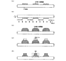
本実の形態5では、本発明の半導体装置のうちアクティブマトリクス型の発光装置の外観図について、図8により説明する。なお、図8(A)は、発光装置を示す上面図、図8(B)は図8(A)をA−A’で切断した断面図である。点線で示された801は駆動回路部(ソース側駆動回路)、802は画素部、803は駆動回路部(ゲート側駆動回路)である。また、804は封止基板、805はシール剤であり、シール剤805で囲まれた内側807は、空間になっている。
本発明の配線を用いて作製された半導体装置を用いて様々な電気器具を完成させることができる。その具体例について図9を用いて説明する。
102 第1の導電膜
103 マスク
104 第2の導電膜
105 レジスト
106 配線
Claims (9)
- 銅の拡散に対するバリア性を有する第1の導電膜をエッチング法により所望の形状とし、
所望の形状とした前記第1の導電膜上に、開口部を有するマスクを用いて銅を主成分とする第2の導電膜を形成し、
ドライエッチング法により前記第2の導電膜の幅を細くして、前記第1の導電膜及び前記第2の導電膜の積層膜からなる配線を形成することを特徴とする半導体装置の作製方法。 - 絶縁表面上に半導体層を形成し、
前記半導体層上にゲート絶縁膜を形成し、
前記ゲート絶縁膜上に銅の拡散に対するバリア性を有する第1の導電膜を形成し、
前記第1の導電膜をエッチング法により所望の形状とし、
所望の形状とした前記第1の導電膜上に開口部を有するマスクを用いて銅を主成分とする第2の導電膜を形成し、
ドライエッチング法により前記第2の導電膜の幅を細くして、前記第1の導電膜及び前記第2の導電膜の積層膜からなる配線を形成することを特徴とする半導体装置の作製方法。 - 請求項1または請求項2において、前記第1の導電膜として、TiN、TaN、WN、
TiC、TaC、または珪素を含む導電膜を用いることを特徴とする半導体装置の作製方法。 - 請求項1または請求項2において、前記第1の導電膜として、TiN、TaN、WN、
TiC、TaC、または珪素を含む導電膜のいずれか一種とTiを主成分とする材料との積層膜を用いることを特徴とする半導体装置の作製方法。 - 請求項1または請求項2において、前記第1の導電膜として、Ti、Al、Ta、Wのいずれか一種又は複数種で形成された導電膜上に、TiN、TaN、WN、TiC、TaC、または珪素を含む導電膜のいずれか一種からなる導電膜が形成された積層膜を用いることを特徴とする半導体装置の作製方法。
- 請求項1乃至5のいずれか一において、前記第2の導電膜を覆って、窒化珪素、窒化酸化珪素、窒化アルミニウム、窒化酸化アルミニウム、ダイヤモンドライクカーボン膜、または窒化炭素からなる絶縁膜を形成することを特徴とする半導体装置の作製方法。
- 請求項1乃至6のいずれか一において、前記第1の導電膜の幅は、30〜40μmであることを特徴とする半導体装置の作製方法。
- 請求項1乃至7のいずれか一において、前記第2の導電膜の幅は、5〜20μmであることを特徴とする半導体装置の作製方法。
- 請求項1乃至8のいずれか一において、前記第2の導電膜の膜厚は、0.1〜1μmであることを特徴とする半導体装置の作製方法。
Priority Applications (1)
| Application Number | Priority Date | Filing Date | Title |
|---|---|---|---|
| JP2003326611A JP4663224B2 (ja) | 2002-09-20 | 2003-09-18 | 半導体装置の作製方法 |
Applications Claiming Priority (2)
| Application Number | Priority Date | Filing Date | Title |
|---|---|---|---|
| JP2002276379 | 2002-09-20 | ||
| JP2003326611A JP4663224B2 (ja) | 2002-09-20 | 2003-09-18 | 半導体装置の作製方法 |
Publications (3)
| Publication Number | Publication Date |
|---|---|
| JP2004134788A JP2004134788A (ja) | 2004-04-30 |
| JP2004134788A5 JP2004134788A5 (ja) | 2006-10-19 |
| JP4663224B2 true JP4663224B2 (ja) | 2011-04-06 |
Family
ID=32301800
Family Applications (1)
| Application Number | Title | Priority Date | Filing Date |
|---|---|---|---|
| JP2003326611A Expired - Fee Related JP4663224B2 (ja) | 2002-09-20 | 2003-09-18 | 半導体装置の作製方法 |
Country Status (1)
| Country | Link |
|---|---|
| JP (1) | JP4663224B2 (ja) |
Families Citing this family (10)
| Publication number | Priority date | Publication date | Assignee | Title |
|---|---|---|---|---|
| US7491590B2 (en) | 2004-05-28 | 2009-02-17 | Semiconductor Energy Laboratory Co., Ltd. | Method for manufacturing thin film transistor in display device |
| JP2006113568A (ja) * | 2004-09-17 | 2006-04-27 | Semiconductor Energy Lab Co Ltd | 表示装置、及び表示装置の作製方法 |
| JP2006114493A (ja) * | 2004-09-17 | 2006-04-27 | Semiconductor Energy Lab Co Ltd | 発光装置 |
| US8350466B2 (en) | 2004-09-17 | 2013-01-08 | Semiconductor Energy Laboratory Co., Ltd. | Display device and manufacturing method thereof |
| CN1819300B (zh) * | 2004-09-17 | 2010-06-16 | 株式会社半导体能源研究所 | 发光器件 |
| JP5182600B2 (ja) * | 2005-09-30 | 2013-04-17 | セイコーエプソン株式会社 | アレイ基板の製造方法 |
| JP4351695B2 (ja) * | 2006-11-27 | 2009-10-28 | エルジー ディスプレイ カンパニー リミテッド | 有機el表示装置 |
| TWI617029B (zh) | 2009-03-27 | 2018-03-01 | 半導體能源研究所股份有限公司 | 半導體裝置 |
| JP2012255840A (ja) * | 2011-06-07 | 2012-12-27 | Japan Display West Co Ltd | 表示装置および電子機器 |
| WO2018123955A1 (ja) * | 2016-12-28 | 2018-07-05 | 三井金属鉱業株式会社 | 配線構造及びその製造方法、スパッタリングターゲット材、並びに酸化防止方法 |
Citations (4)
| Publication number | Priority date | Publication date | Assignee | Title |
|---|---|---|---|---|
| JP2001049423A (ja) * | 1999-08-02 | 2001-02-20 | Nippon Telegr & Teleph Corp <Ntt> | 金属膜の形成方法 |
| JP2002108243A (ja) * | 2000-06-05 | 2002-04-10 | Semiconductor Energy Lab Co Ltd | 表示パネル、検査方法及び該表示パネルの作製方法 |
| JP2002261007A (ja) * | 2001-02-28 | 2002-09-13 | Semiconductor Energy Lab Co Ltd | 半導体装置の作製方法 |
| JP2003328126A (ja) * | 2002-05-09 | 2003-11-19 | Konica Minolta Holdings Inc | パターニング方法及び製膜装置 |
Family Cites Families (4)
| Publication number | Priority date | Publication date | Assignee | Title |
|---|---|---|---|---|
| JPH03195087A (ja) * | 1989-12-25 | 1991-08-26 | Matsushita Electric Works Ltd | 金属層積層無機質基板への回路パターンの形成方法 |
| JPH04348035A (ja) * | 1991-05-24 | 1992-12-03 | Nippon Steel Corp | 配線形成方法 |
| JPH0566421A (ja) * | 1991-09-09 | 1993-03-19 | Sanyo Electric Co Ltd | 多層配線の形成方法 |
| JPH08274093A (ja) * | 1995-03-29 | 1996-10-18 | Oki Electric Ind Co Ltd | 半導体素子の金属配線形成方法 |
-
2003
- 2003-09-18 JP JP2003326611A patent/JP4663224B2/ja not_active Expired - Fee Related
Patent Citations (4)
| Publication number | Priority date | Publication date | Assignee | Title |
|---|---|---|---|---|
| JP2001049423A (ja) * | 1999-08-02 | 2001-02-20 | Nippon Telegr & Teleph Corp <Ntt> | 金属膜の形成方法 |
| JP2002108243A (ja) * | 2000-06-05 | 2002-04-10 | Semiconductor Energy Lab Co Ltd | 表示パネル、検査方法及び該表示パネルの作製方法 |
| JP2002261007A (ja) * | 2001-02-28 | 2002-09-13 | Semiconductor Energy Lab Co Ltd | 半導体装置の作製方法 |
| JP2003328126A (ja) * | 2002-05-09 | 2003-11-19 | Konica Minolta Holdings Inc | パターニング方法及び製膜装置 |
Also Published As
| Publication number | Publication date |
|---|---|
| JP2004134788A (ja) | 2004-04-30 |
Similar Documents
| Publication | Publication Date | Title |
|---|---|---|
| US7585761B2 (en) | Manufacturing method of semiconductor device | |
| US10381385B2 (en) | Display device and method for manufacturing the same | |
| JP6691190B2 (ja) | 発光装置 | |
| JP4663257B2 (ja) | 発光装置及びその作製方法 | |
| TWI338366B (en) | Display device and manufacturing method thereof | |
| US8669663B2 (en) | Wiring over substrate, semiconductor device, and methods for manufacturing thereof | |
| US6744198B2 (en) | Method for manufacturing display device, display device, and electronic apparatus | |
| US8344379B2 (en) | Display device and manufacturing method of the same | |
| TW200402679A (en) | Electro-optical device and electronic apparatus | |
| JP2001102169A (ja) | El表示装置 | |
| JP4663224B2 (ja) | 半導体装置の作製方法 | |
| US6744217B2 (en) | Organic electro luminescence device | |
| JP4439861B2 (ja) | 表示装置の作製方法 | |
| CN101414610B (zh) | 显示单元以及该显示单元的制造方法 | |
| US20080079887A1 (en) | System for displaying images including wiring structure for driving display panel | |
| US20170207287A1 (en) | Display device | |
| JP3956959B2 (ja) | 有機el装置及び電子機器 | |
| US11037963B2 (en) | Thin film transistor and method for manufacturing the same, and display device including the same | |
| US7034442B2 (en) | Electro-optical device, method of manufacturing the same, and electronic instrument | |
| JP2006018084A (ja) | 自発光装置及び電子機器 | |
| CN112447798A (zh) | 显示设备 | |
| JP2005327745A (ja) | 発光装置及びその作製方法 |
Legal Events
| Date | Code | Title | Description |
|---|---|---|---|
| A521 | Request for written amendment filed |
Free format text: JAPANESE INTERMEDIATE CODE: A523 Effective date: 20060901 |
|
| A621 | Written request for application examination |
Free format text: JAPANESE INTERMEDIATE CODE: A621 Effective date: 20060901 |
|
| A977 | Report on retrieval |
Free format text: JAPANESE INTERMEDIATE CODE: A971007 Effective date: 20090929 |
|
| A131 | Notification of reasons for refusal |
Free format text: JAPANESE INTERMEDIATE CODE: A131 Effective date: 20100720 |
|
| A521 | Request for written amendment filed |
Free format text: JAPANESE INTERMEDIATE CODE: A523 Effective date: 20100903 |
|
| A131 | Notification of reasons for refusal |
Free format text: JAPANESE INTERMEDIATE CODE: A131 Effective date: 20101102 |
|
| A521 | Request for written amendment filed |
Free format text: JAPANESE INTERMEDIATE CODE: A523 Effective date: 20101129 |
|
| TRDD | Decision of grant or rejection written | ||
| A01 | Written decision to grant a patent or to grant a registration (utility model) |
Free format text: JAPANESE INTERMEDIATE CODE: A01 Effective date: 20101221 |
|
| A01 | Written decision to grant a patent or to grant a registration (utility model) |
Free format text: JAPANESE INTERMEDIATE CODE: A01 |
|
| A61 | First payment of annual fees (during grant procedure) |
Free format text: JAPANESE INTERMEDIATE CODE: A61 Effective date: 20110105 |
|
| R150 | Certificate of patent or registration of utility model |
Ref document number: 4663224 Country of ref document: JP Free format text: JAPANESE INTERMEDIATE CODE: R150 Free format text: JAPANESE INTERMEDIATE CODE: R150 |
|
| FPAY | Renewal fee payment (event date is renewal date of database) |
Free format text: PAYMENT UNTIL: 20140114 Year of fee payment: 3 |
|
| R250 | Receipt of annual fees |
Free format text: JAPANESE INTERMEDIATE CODE: R250 |
|
| R250 | Receipt of annual fees |
Free format text: JAPANESE INTERMEDIATE CODE: R250 |
|
| R250 | Receipt of annual fees |
Free format text: JAPANESE INTERMEDIATE CODE: R250 |
|
| R250 | Receipt of annual fees |
Free format text: JAPANESE INTERMEDIATE CODE: R250 |
|
| R250 | Receipt of annual fees |
Free format text: JAPANESE INTERMEDIATE CODE: R250 |
|
| R250 | Receipt of annual fees |
Free format text: JAPANESE INTERMEDIATE CODE: R250 |
|
| R250 | Receipt of annual fees |
Free format text: JAPANESE INTERMEDIATE CODE: R250 |
|
| R250 | Receipt of annual fees |
Free format text: JAPANESE INTERMEDIATE CODE: R250 |
|
| R250 | Receipt of annual fees |
Free format text: JAPANESE INTERMEDIATE CODE: R250 |
|
| LAPS | Cancellation because of no payment of annual fees |