JP4637315B2 - Display device - Google Patents
Display device Download PDFInfo
- Publication number
- JP4637315B2 JP4637315B2 JP2000039258A JP2000039258A JP4637315B2 JP 4637315 B2 JP4637315 B2 JP 4637315B2 JP 2000039258 A JP2000039258 A JP 2000039258A JP 2000039258 A JP2000039258 A JP 2000039258A JP 4637315 B2 JP4637315 B2 JP 4637315B2
- Authority
- JP
- Japan
- Prior art keywords
- film
- video data
- display device
- circuit
- digital video
- Prior art date
- Legal status (The legal status is an assumption and is not a legal conclusion. Google has not performed a legal analysis and makes no representation as to the accuracy of the status listed.)
- Expired - Fee Related
Links
Images


Classifications
-
- G—PHYSICS
- G09—EDUCATION; CRYPTOGRAPHY; DISPLAY; ADVERTISING; SEALS
- G09G—ARRANGEMENTS OR CIRCUITS FOR CONTROL OF INDICATING DEVICES USING STATIC MEANS TO PRESENT VARIABLE INFORMATION
- G09G3/00—Control arrangements or circuits, of interest only in connection with visual indicators other than cathode-ray tubes
- G09G3/20—Control arrangements or circuits, of interest only in connection with visual indicators other than cathode-ray tubes for presentation of an assembly of a number of characters, e.g. a page, by composing the assembly by combination of individual elements arranged in a matrix no fixed position being assigned to or needed to be assigned to the individual characters or partial characters
- G09G3/2007—Display of intermediate tones
- G09G3/2018—Display of intermediate tones by time modulation using two or more time intervals
- G09G3/2022—Display of intermediate tones by time modulation using two or more time intervals using sub-frames
- G09G3/2025—Display of intermediate tones by time modulation using two or more time intervals using sub-frames the sub-frames having all the same time duration
-
- G—PHYSICS
- G09—EDUCATION; CRYPTOGRAPHY; DISPLAY; ADVERTISING; SEALS
- G09G—ARRANGEMENTS OR CIRCUITS FOR CONTROL OF INDICATING DEVICES USING STATIC MEANS TO PRESENT VARIABLE INFORMATION
- G09G3/00—Control arrangements or circuits, of interest only in connection with visual indicators other than cathode-ray tubes
- G09G3/20—Control arrangements or circuits, of interest only in connection with visual indicators other than cathode-ray tubes for presentation of an assembly of a number of characters, e.g. a page, by composing the assembly by combination of individual elements arranged in a matrix no fixed position being assigned to or needed to be assigned to the individual characters or partial characters
- G09G3/2007—Display of intermediate tones
- G09G3/2077—Display of intermediate tones by a combination of two or more gradation control methods
- G09G3/2081—Display of intermediate tones by a combination of two or more gradation control methods with combination of amplitude modulation and time modulation
-
- G—PHYSICS
- G09—EDUCATION; CRYPTOGRAPHY; DISPLAY; ADVERTISING; SEALS
- G09G—ARRANGEMENTS OR CIRCUITS FOR CONTROL OF INDICATING DEVICES USING STATIC MEANS TO PRESENT VARIABLE INFORMATION
- G09G3/00—Control arrangements or circuits, of interest only in connection with visual indicators other than cathode-ray tubes
- G09G3/20—Control arrangements or circuits, of interest only in connection with visual indicators other than cathode-ray tubes for presentation of an assembly of a number of characters, e.g. a page, by composing the assembly by combination of individual elements arranged in a matrix no fixed position being assigned to or needed to be assigned to the individual characters or partial characters
- G09G3/34—Control arrangements or circuits, of interest only in connection with visual indicators other than cathode-ray tubes for presentation of an assembly of a number of characters, e.g. a page, by composing the assembly by combination of individual elements arranged in a matrix no fixed position being assigned to or needed to be assigned to the individual characters or partial characters by control of light from an independent source
- G09G3/36—Control arrangements or circuits, of interest only in connection with visual indicators other than cathode-ray tubes for presentation of an assembly of a number of characters, e.g. a page, by composing the assembly by combination of individual elements arranged in a matrix no fixed position being assigned to or needed to be assigned to the individual characters or partial characters by control of light from an independent source using liquid crystals
- G09G3/3611—Control of matrices with row and column drivers
- G09G3/3685—Details of drivers for data electrodes
- G09G3/3688—Details of drivers for data electrodes suitable for active matrices only
-
- G—PHYSICS
- G09—EDUCATION; CRYPTOGRAPHY; DISPLAY; ADVERTISING; SEALS
- G09G—ARRANGEMENTS OR CIRCUITS FOR CONTROL OF INDICATING DEVICES USING STATIC MEANS TO PRESENT VARIABLE INFORMATION
- G09G2310/00—Command of the display device
- G09G2310/02—Addressing, scanning or driving the display screen or processing steps related thereto
- G09G2310/0235—Field-sequential colour display
-
- G—PHYSICS
- G09—EDUCATION; CRYPTOGRAPHY; DISPLAY; ADVERTISING; SEALS
- G09G—ARRANGEMENTS OR CIRCUITS FOR CONTROL OF INDICATING DEVICES USING STATIC MEANS TO PRESENT VARIABLE INFORMATION
- G09G2310/00—Command of the display device
- G09G2310/02—Addressing, scanning or driving the display screen or processing steps related thereto
- G09G2310/0264—Details of driving circuits
- G09G2310/027—Details of drivers for data electrodes, the drivers handling digital grey scale data, e.g. use of D/A converters
-
- G—PHYSICS
- G09—EDUCATION; CRYPTOGRAPHY; DISPLAY; ADVERTISING; SEALS
- G09G—ARRANGEMENTS OR CIRCUITS FOR CONTROL OF INDICATING DEVICES USING STATIC MEANS TO PRESENT VARIABLE INFORMATION
- G09G3/00—Control arrangements or circuits, of interest only in connection with visual indicators other than cathode-ray tubes
- G09G3/20—Control arrangements or circuits, of interest only in connection with visual indicators other than cathode-ray tubes for presentation of an assembly of a number of characters, e.g. a page, by composing the assembly by combination of individual elements arranged in a matrix no fixed position being assigned to or needed to be assigned to the individual characters or partial characters
- G09G3/34—Control arrangements or circuits, of interest only in connection with visual indicators other than cathode-ray tubes for presentation of an assembly of a number of characters, e.g. a page, by composing the assembly by combination of individual elements arranged in a matrix no fixed position being assigned to or needed to be assigned to the individual characters or partial characters by control of light from an independent source
- G09G3/36—Control arrangements or circuits, of interest only in connection with visual indicators other than cathode-ray tubes for presentation of an assembly of a number of characters, e.g. a page, by composing the assembly by combination of individual elements arranged in a matrix no fixed position being assigned to or needed to be assigned to the individual characters or partial characters by control of light from an independent source using liquid crystals
- G09G3/3611—Control of matrices with row and column drivers
- G09G3/3648—Control of matrices with row and column drivers using an active matrix
- G09G3/3651—Control of matrices with row and column drivers using an active matrix using multistable liquid crystals, e.g. ferroelectric liquid crystals
Description
【0001】
【発明の属する技術分野】
【0002】
本発明は、表示装置に関する。特に、階調電圧と時間階調との両方によって階調表示を行う表示装置に関する。
【0003】
【従来の技術】
【0004】
最近安価なガラス基板上に半導体薄膜を形成した半導体装置、例えば薄膜トランジスタ(TFT)を作製する技術が急速に発達してきている。その理由は、アクティブマトリクス型表示装置の需要が高まってきたことによる。
【0005】
アクティブマトリクス型表示装置は、マトリクス状に配置された数十〜数百万個もの画素領域にそれぞれ画素TFTが配置され、各画素TFTに接続された画素電極に出入りする電荷を画素TFTのスイッチング機能により制御するものである。
【0006】
近年、画像の高精細化、高解像度化とともに、望ましくはフルカラー表示が行える多階調表示が求められている。
【0007】
また、アクティブマトリクス型表示装置の中でも、表示装置の高精細化、高解像度化に伴い、高速駆動が可能なデジタル駆動方式のアクティブマトリクス型表示装置が注目されてきている。
【0008】
【発明が解決しようとする課題】
【0009】
デジタル駆動方式のアクティブマトリクス型表示装置には、外部から入力されるデジタルビデオデータをアナログデータ(階調電圧)に変換するD/A変換回路(DAC)が必要である。D/A変換回路には、様々な種類のものが存在する。
【0010】
アクティブマトリクス型表示装置の多階調表示能力は、このD/A変換回路の能力、つまりD/A変換回路が何ビットのデジタルビデオデータをアナログデータに変換することができるかに依存している。例えば、一般的に、2ビットのデジタルビデオデータを処理するD/A変換回路を有する表示装置であれば、22=4階調表示を行うことができ、8ビットならば28=256階調表示を行うことができ、またnビットならば2n階調表示を行うことができる。
【0011】
しかし、D/A変換回路の能力を上げるためには、D/A変換回路の回路構成が複雑になり、かつレイアウト面積が大きくなる。最近では、D/A変換回路をアクティブマトリクス回路と同一基板上にポリシリコンTFTによって形成する表示装置が報告されてきている。しかし、この場合、D/A変換回路の回路構成が複雑になると、D/A変換回路の歩留まりが低下し、表示装置の歩留まりも低下してしまう。また、D/A変換回路のレイアウト面積が大きくなると、小型の表示装置を実現することが困難になる。
【0012】
【課題を解決するための手段】
【0013】
そこで、本発明は上述の問題に鑑みてなされたものであり、多階調の表示を実現することのできる表示装置を提供するものである。
【0014】
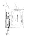
まず、図1を参照する。図1には、本発明の表示装置の概略構成図が示されている。101はデジタルドライバを有する表示パネルである。101−1はソースドライバであり、101−2および101−3はゲートドライバであり、101−4は複数の画素TFTがマトリクス状に配置されたアクティブマトリクス回路である。ソースドライバ101−1およびゲートドライバ101−2ならびに101−3は、アクティブマトリクス回路を駆動する。102はデジタルビデオデータ時間階調処理回路である。
【0015】
デジタルビデオデータ時間階調処理回路102は、外部から入力されるmビットデジタルビデオデータのうちnビットのデジタルビデオデータを、nビットの階調電圧の為のデジタルビデオデータに変換する。mビットのデジタルビデオデータのうち下位(m−n)ビットの階調情報は、時間階調によって表現される。
【0016】
デジタルビデオデータ時間階調処理回路102によって変換されたnビットデジタルビデオデータは、表示パネル101に入力される。表示パネル101に入力されたnビットデジタルビデオデータは、ソースドライバに入力され、ソースドライバ内のD/A変換回路でアナログ階調データに変換され、各ソース信号線に供給される。
【0017】
次に、本発明の表示装置の別の例を図2に示す。図2において、201はアナログドライバを有する表示パネルである。201−1はソースドライバであり、201−2および201−3はゲートドライバであり、201−4は複数の画素TFTがマトリクス状に配置されたアクティブマトリクス回路である。ソースドライバ201−1およびゲートドライバ201−2ならびに201−3は、アクティブマトリクス回路を駆動する。202はA/D変換回路であり、外部から供給されるアナログビデオデータをmビットデジタルビデオデータに変換する。203はデジタルビデオデータ時間階調処理回路である。デジタルビデオデータ時間階調処理回路203は、入力されるmビットデジタルビデオデータのうちnビットのデジタルビデオデータを、nビットの階調電圧の為のデジタルビデオデータに変換する。入力されるmビットのデジタルビデオデータのうち下位(m−n)ビットの階調情報は、時間階調によって表現される。デジタルビデオデータ時間階調処理回路203によって変換されたnビットデジタルビデオデータは、D/A変換回路204に入力され、アナログビデオデータに変換される。D/A変換回路204によって変換されたアナログビデオデータは、表示パネル201に入力される。表示パネル201に入力されたアナログビデオデータは、ソースドライバに入力され、ソースドライバ内のサンプリング回路によってサンプリングされ、各ソース信号線に供給される。
【0018】
なお、本発明の表示装置の動作の詳細について実施形態を用いて後述することにする。
【0019】
以下に本発明の構成を述べる。
【0020】
本発明によると、
複数の画素TFTがマトリクス状に配置されたアクティブマトリクス回路と、
前記アクティブマトリクス回路を駆動するソースドライバおよびゲートドライバと、
を有する表示装置であって、
外部から入力されるmビットデジタルビデオデータのうち、上位nビットを階調電圧の情報として、かつ下位(m−n)ビットを時間階調の情報として用い、m、nは共に2以上の正数、かつm>nであることを特徴とする表示装置が提供される。。
【0021】
また、本発明によると、
複数の画素TFTがマトリクス状に配置されたアクティブマトリクス回路と、
前記アクティブマトリクス回路を駆動するソースドライバおよびゲートドライバと、
外部から入力されるmビットデジタルビデオデータを階調電圧のためのnビットデジタルビデオデータに変換し、前記ソースドライバに前記nビットデジタルビデオデータを供給する回路と(m、nは共に2以上の正数、m>n)、
を有する表示装置であって、
2m-n個のサブフレームによって1フレームの映像を形成することによって時間階調表示を行うことを特徴とする表示装置が提供される。
【0022】
また、本発明によると、
複数の画素TFTがマトリクス状に配置されたアクティブマトリクス回路と、
前記アクティブマトリクス回路を駆動するソースドライバおよびゲートドライバと、
外部から入力されるmビットデジタルビデオデータを階調電圧のためのnビットデジタルビデオデータに変換し、前記ソースドライバに前記nビットデジタルビデオデータを供給する回路と(m、nは共に2以上の正数、m>n)、
を有する表示装置であって、
2m-n個のサブフレームによって1フレームの映像を形成することによって時間階調表示を行い、(2m−(2m-n−1))通りの階調表示を得ることを特徴とする表示装置が提供される。
【0023】
また、本発明によると、
複数の画素TFTがマトリクス状に配置されたアクティブマトリクス回路と、
前記アクティブマトリクス回路を駆動するソースドライバおよびゲートドライバと、
を有する表示装置であって、
外部から入力されるmビットデジタルビデオデータのうち、上位nビットを階調電圧の情報として、かつ下位(m−n)ビットを時間階調の情報として用い(m、nは共に2以上の正数、m>n)、
前記ソースドライバは、前記nビットデジタルビデオデータをアナログ階調電圧に変換するD/A変換回路を有していることを特徴とする表示装置が提供される。
【0024】
また、本発明によると、
複数の画素TFTがマトリクス状に配置されたアクティブマトリクス回路と、
前記アクティブマトリクス回路を駆動するソースドライバおよびゲートドライバと、
外部から入力されるmビットデジタルビデオデータを階調電圧のためのnビットデジタルビデオデータに変換し、前記ソースドライバに前記nビットデジタルビデオデータを供給する回路と(m、nは共に2以上の正数、m>n)、
を有する表示装置であって、
前記ソースドライバは、前記nビットデジタルビデオデータをアナログ階調電圧に変換するD/A変換回路を有しており、
2m-n個のサブフレームによって1フレームの映像を形成することによって時間階調表示を行うことを特徴とする表示装置が提供される。
【0025】
また、本発明によると、
複数の画素TFTがマトリクス状に配置されたアクティブマトリクス回路と、
前記アクティブマトリクス回路を駆動するソースドライバおよびゲートドライバと、
外部から入力されるmビットデジタルビデオデータを階調電圧のためのnビットデジタルビデオデータに変換し、前記ソースドライバに前記nビットデジタルビデオデータを供給する回路と(m、nは共に2以上の正数、m>n)、
を有する表示装置であって、
前記ソースドライバは、前記nビットデジタルビデオデータをアナログ階調電圧に変換するD/A変換回路を有しており、
2m-n個のサブフレームによって1フレームの映像を形成することによって時間階調表示を行い、(2m−(2m-n−1))通りの階調表示を得ることを特徴とする表示装置が提供される。
【0026】
また、本発明によると、
複数の画素TFTがマトリクス状に配置されたアクティブマトリクス回路と、
前記アクティブマトリクス回路を駆動するソースドライバおよびゲートドライバと、
外部から入力されるmビットデジタルビデオデータを階調電圧のためのnビットデジタルビデオデータに変換する回路と(m、nは共に2以上の正数、m>n)、
前記nビットデジタルビデオデータをアナログビデオデータに変換し、前記ソースドライバに入力するするD/A変換回路と、
を有する表示装置であって、
2m-n個のサブフレームによって1フレームの映像を形成することによって時間階調表示を行うことを特徴とする表示装置が提供される。
【0027】
また、本発明によると、
複数の画素TFTがマトリクス状に配置されたアクティブマトリクス回路と、
前記アクティブマトリクス回路を駆動するソースドライバおよびゲートドライバと、
外部から入力されるmビットデジタルビデオデータを階調電圧のためのnビットデジタルビデオデータに変換する回路と(m、nは共に2以上の正数、m>n)、
前記nビットデジタルビデオデータをアナログビデオデータに変換し、前記ソースドライバに入力するするD/A変換回路と、
を有する表示装置であって、
2m-n個のサブフレームによって1フレームの映像を形成することによって時間階調表示を行い、(2m−(2m-n−1))通りの階調表示を得ることを特徴とする表示装置が提供される。
【0028】
前記mは8、前記nは2であってもよい。
【0029】
前記mは10、前記nは2であってもよい。
【0030】
前記mは12、前記nは4であってもよい。
【0031】
【発明の実施の形態】
【0032】
以下に本発明の表示装置を実施形態をもって説明する。ただし、本発明の表示装置は、以下の実施形態に限定されるわけではない。
【0033】
(実施形態1)
【0034】
本実施形態の表示装置の概略構成図を図3に示す。本実施形態においては、説明の簡略のため、外部から4ビットデジタルビデオデータが供給される表示装置を例にとる。
【0035】
301はデジタルドライバを有する表示パネルである。301−1はソースドライバであり、301−2および301−3はゲートドライバであり、301−4は複数の画素TFTがマトリクス状に配置されたアクティブマトリクス回路である。
【0036】
デジタルビデオデータ時間階調処理回路302は、外部から入力される4ビットデジタルビデオデータのうち上位2ビットのデジタルビデオデータを、2ビットの階調電圧の為のデジタルビデオデータに変換する。4ビットのデジタルビデオデータのうち下位2ビットの階調情報は、時間階調によって表現される。
【0037】
デジタルビデオデータ時間階調処理回路302によって変換された上位2ビットデジタルビデオデータは、表示パネル301に入力される。表示パネル301に入力された2ビットデジタルビデオデータは、ソースドライバに入力され、ソースドライバ内のD/A変換回路(図示せず)でアナログ階調データに変換され、各ソース信号線に供給される。なお、本実施形態の表示パネルに内蔵されるD/A変換回路は、2ビットのデジタルビデオデータをアナログ階調電圧に変換する。
【0038】
ここで、本実施形態の表示パネルが表示媒体として液晶を用いた液晶パネルである場合について説明する。
表示パネル301の回路構成、特にアクティブマトリクス回路301−4について、図4を用いて説明する。
【0039】
アクティブマトリクス回路301−4は、(x×y)個の画素を有している。
それぞれの画素には、説明の便宜上、P1,1、P2,1、・・・、Py,x等の符号が付けられている。また、それぞれの画素は、画素TFT301−4−1、保持容量301−4−3を有している。また、ソースドライバ301−1、ゲートドライバ301−2ならびに301−3、およびアクティブマトリクス回路301−4が形成されているアクティブマトリクス基板と対向基板との間には、液晶が挟まれている。液晶3006は、各画素に対応する液晶を模式的に示したものである。
【0040】
本実施形態のデジタルドライバ表示パネルは、1ライン分の画素(例えば、P1,1、P1,2、・・・、P1,x)を同時に駆動する、いわゆる線順次駆動を行う。言い換えると、1ライン分の画素に同時にアナログ階調電圧を書き込む。全ての画素(P1,1〜Py,x)にアナログ階調電圧を書き込むのに要する時間を1フレーム期間(Tf)と呼ぶことにする。また、1フレーム期間(Tf)を4分割した期間をサブフレーム期間(Tsf)と呼ぶことにする。さらに、1ライン分の画素(例えば、P1,1、P1,2、・・・、P1,x)にアナログ階調電圧を書き込むのに要する時間を1ライン期間(Tsfl)と呼ぶことにする。
【0041】
本実施形態の表示装置の階調表示について説明する。本実施形態の表示装置に外部から供給されるデジタルビデオデータは、4ビットであり、16階調の情報を有している。ここで、図5を参照する。図5には、本実施形態の表示装置の階調表示レベルが示されている。電圧レベルVLはD/A変換回路に入力される最低の電圧レベルであり、また、電圧レベルVHはD/A変換回路に入力される最高の電圧レベルである。
【0042】
本実施形態においては、4階調の電圧レベルを実現するために、電圧レベルVHと電圧レベルVLとの間をほぼ等電圧レベルに分割し、その電圧レベルのステップをαとした。なお、α=(VH−VL)/4である。よって、本実施形態のD/A変換回路が出力する階調電圧レベルは、デジタルビデオデータのアドレスが(00)の時はVLとなり、デジタルビデオデータのアドレスが(01)の時はVL+αとなり、デジタルビデオデータのアドレスが(10)の時はVL+2αとなり、デジタルビデオデータのアドレスが(11)の時はVL+3αとなる。
【0043】
本実施形態のD/A変換回路が出力できる階調電圧レベルは、上述の様にVL、VL+α、VL+2α、およびVL+3αの4通りである。そこで、本発明においては、時間階調表示を組合わせることによって、表示装置の階調表示レベルの数を上げることができる。本実施形態においては、4ビットデジタルビデオデータのうちの2ビット分の情報を時間階調表示にもちいることによって、電圧レベルのステップαをほぼ4等分した階調電圧レベルに相当する階調表示レベルを実現することができる。つまり、本実施形態の表示装置は、VL、VL+α/4、VL+2α/4、VL+3α/4、VL+α、VL+5α/4、VL+6α/4、VL+7α/4、VL+2α、VL+9α/4、VL+10α/4、VL+11α/4、VL+3αの階調電圧レベルに相当する階調表示レベルを実現することができる。
【0044】
ここで、外部から入力される4ビットデジタルビデオデータアドレスと、時間階調処理後デジタルビデオデータアドレスおよびそれに対応する階調電圧レベルと、時間階調を組み合わせた階調表示レベルとの対応を下記の表1に示す。
【0045】
【表1】

本実施形態の表示装置は、1フレーム期間Tfを4つのサブフレーム期間(1st Tsf、2nd Tsf、3rd Tsf、および4th Tsf)に分割して表示を行っている。さらに、本実施形態の表示装置は、線順次駆動を行うので、各画素は1ライン期間(Tsfl)の間、階調電圧が書き込まれる。よって、各サブフレーム期間(1stTsf、2nd Tsf、3rd Tsf、および4th Tsf)に対応する各サブフレームライン期間(1st Tsfl、2nd Tsfl、3rd Tsfl、および4th Tsfl)に、時間階調処理後の2ビットデジタルビデオデータのアドレスがD/A変換回路に入力され、D/A変換回路から階調電圧が出力される。4つのサブフレームライン期間(1st Tsfl、2nd Tsfl、3rd Tsfl、および4th Tsfl)に書き込まれる階調電圧によって4回のサブフレームの表示が高速に行われ、結果として1フレームの階調表示は、各サブフレームライン期間の階調電圧レベルの総和を時間平均したものになる。
【0047】
なお、表1に示すように、本実施形態においては、4ビットデジタルビデオデータのアドレスが(1100)〜(1111)までは同じ階調電圧レベル(VL+3α)が出力される。
【0048】
よって、本実施形態の表示装置においては、2ビットデジタルビデオデータを扱うD/A変換回路をした場合でも、24−3=13階調の階調レベルの表示を行うことができる。
【0049】
図6には、本実施形態の表示装置の駆動タイミングチャートが示されている。
図6には、画素P1,1〜画素Py,1が例にとって示されている。
【0050】
画素P1,1を例にとって説明すると、画素P1,1には、各サブフレームライン期間(1st Tsfl、2nd Tsfl、3rd Tsfl、および4th Tsfl)に、デジタルビデオデータ1,1-1、1,1-2、1,1-3、および1,1-4がそれぞれ書き込まれる。これらのデジタルビデオデータ1,1-1、1,1-2、1,1-3、および1,1-4は、4ビットのデジタルビデオデータ1,1を時間階調処理した2ビットデジタルビデオデータである。
【0051】
このような動作が、全ての画素について行われる。
【0052】
ここで、図7を参照する。図7は、ある画素(例えば、画素P1,1)に書き込まれる階調電圧レベルと、サブフレーム期間およびフレーム期間との関係を示したものである。
【0053】
まず、1フレーム期間目に着目すると、第1のサブフレームライン期間(1st Tsfl)にはVL+αの階調電圧が書き込まれ、第1のサブフレーム期間(1st Tsf)には階調電圧VL+αに対応した画像が表示される。次に、第2のサブフレームライン期間(2nd Tsfl)にはVL+2αの階調電圧が書き込まれ、第2のサブフレーム期間(2nd Tsf)には階調電圧VL+2αに対応した画像が表示される。次に、第3のサブフレームライン期間(3rd Tsfl)にはVL+2αの階調電圧が書き込まれ、第3のサブフレーム期間(3rd Tsf)には階調電圧VL+2αに対応した画像が表示される。次に、第4のサブフレームライン期間(4th Tsfl)にはVL+2αの階調電圧が書き込まれ、第4のサブフレーム期間(4th Tsf)には階調電圧VL+2αに対応した画像が表示される。よって、1フレーム目の階調表示レベルは、VL+7α/4の階調電圧レベルに対応した階調表示となる。
【0054】
次に、2フレーム期間目に着目すると、第1のサブフレームライン期間(1st Tsfl)にはVL+2αの階調電圧が書き込まれ、第1のサブフレーム期間(1st Tsf)には階調電圧VL+2αに対応した画像が表示される。次に、第2のサブフレームライン期間(2nd Tsfl)にはVL+2αの階調電圧が書き込まれ、第2のサブフレーム期間(2nd Tsf)には階調電圧VL+2αに対応した画像が表示される。次に、第3のサブフレームライン期間(3rd Tsfl)にはVL+3αの階調電圧が書き込まれ、第3のサブフレーム期間(3rd Tsf)には階調電圧VL+3αに対応した画像が表示される。次に、第4のサブフレームライン期間(4th Tsfl)にはVL+3αの階調電圧が書き込まれ、第4のサブフレーム期間(4th Tsf)には階調電圧VL+3αに対応した画像が表示される。よって、2フレーム目の階調表示レベルは、VL+10α/4の階調電圧レベルに対応した階調表示となる。
【0055】
このように、13通りの階調表示が行われることが理解される。
【0056】
なお、本実施形態においては、4階調の電圧レベルを実現するために、電圧レベルVHと電圧レベルVLとの間をほぼ等電圧レベルに分割し、その電圧レベルのステップをαとしたが、電圧レベルVHと電圧レベルVLとの間を等電圧レベルに分割せず任意に設定した場合でも、本発明の効果はある。
【0057】
また、本実施形態においては、各サブフレームライン期間に書き込まれる階調電圧レベルを表1のように設定したが、下記の表2に示す様にしてもよい。
【0058】
【表2】
また、各サブフレームライン期間(1st Tsfl、2nd Tsfl、3rd Tsfl、および4th Tsfl)に書き込まれるデジタルビデオデータのアドレス(または階調電圧レベル)は、表1または表2以外の組合わせによっても設定され得る。
【0060】
また、本実施形態においては、外部から入力される4ビットデジタルビデオデータのうち上位2ビットのデジタルビデオデータを、2ビットの階調電圧の為のデジタルビデオデータに変換し、4ビットのデジタルビデオデータのうち下位2ビットの階調情報は、時間階調によって表現されるようにした。ここで、一般に、外部からmビットのデジタルビデオデータが時間階調処理回路によって、上位nビットデジタルビデオデータが、階調電圧の為のデジタルビデオデータに変換され、下位(m−n)ビットの階調情報は、時間階調によって表現される場合を考える。なお、m、nは共に2以上の整数であり、m>nとする。
【0061】
この場合、フレーム期間(Tf)とサブフレーム期間(Tsf)との関係は、
Tf=2m-n・Tsf
となり、(2m−(2m-n−1))通りの階調表示を行うことができる。
【0062】
なお、m=12およびn=4でもよい。
【0063】
(実施形態2)
【0064】
本実施形態においては、8ビットデジタルビデオデータが入力される表示装置について説明する。図8を参照する。図8には、本実施形態の表示装置の概略構成図が示されている。801はデジタルドライバを有するパネルである。801−1ならびに801−2はソースドライバであり、801−3はゲートドライバであり、801−4は複数の画素TFTがマトリクス状に配置されたアクティブマトリクス回路であり、801−5はデジタルビデオデータ時間階調処理回路である。
【0065】
デジタルビデオデータ時間階調処理回路801−5は、外部から入力される8ビットデジタルビデオデータのうち6ビットのデジタルビデオデータを、6ビットの階調電圧の為のデジタルビデオデータに変換する。8ビットのデジタルビデオデータのうち2ビットの階調情報は、時間階調によって表現される。
【0066】
デジタルビデオデータ時間階調処理回路801−5によって変換された6ビットデジタルビデオデータは、ソースドライバ801−1および801−2に入力され、ソースドライバ内のD/A変換回路(図示せず)でアナログ階調電圧に変換され、各ソース信号線に供給される。なお、本実施形態の表示装置に内蔵されるD/A変換回路は、6ビットのデジタルビデオデータをアナログ階調電圧に変換する。
【0067】
なお、本実施形態の表示装置においては、ソースドライバ801−1ならびに801−2、ゲートドライバ801−3、アクティブマトリクス回路801−4、およびデジタルビデオデータ時間階調処理回路801−5が同一基板上に一体形成されている。
【0068】
ここで、図9を参照する。図9には、本実施形態の表示装置の回路構成がより詳しく示されている。ソースドライバ801−1は、シフトレジスタ回路801−1−1、ラッチ回路1(801−1−2)、ラッチ回路2(801−1−3)、D/A変換回路(801−1−4)を有している。その他、バッファ回路やレベルシフタ回路(いずれも図示せず)を有している。また、説明の便宜上、D/A変換回路801−1−4にはレベルシフタ回路が含まれている。
【0069】
ソースドライバ801−2は、ソースドライバ801−1と同じ構成を有する。なお、ソースドライバ801−1は、奇数番目のソース信号線に画像信号(階調電圧)を供給し、ソースドライバ801−2は、偶数番目のソース信号線に画像信号を供給するようになっている。
【0070】
なお、本実施形態のアクティブマトリクス型表示装置においては、回路レイアウトの都合上、アクティブマトリクス回路の上下を挟むように2つのソースドライバ801−1および801−2を設けたが、回路レイアウト上、可能であれば、ソースドライバを1つだけ設けるようにしても良い。
【0071】
また、801−3はゲートドライバであり、シフトレジスタ回路、バッファ回路、レベルシフタ回路等(いずれも図示せず)を有している。
【0072】
アクティブマトリクス回路801−4は、1920×1080(横×縦)の画素を有している。各画素の構成は、上記実施形態1で説明したものと同様である。
【0073】
本実施形態の表示装置は、6ビットデジタルビデオデータを扱うD/A変換回路801−1−4を有している。また、外部から供給される8ビットデジタルビデオデータのうち下位2ビット分の情報を時間階調を行うために用いる。なお、時間階調については、上述の実施形態1と同様である。
【0074】
よって、本実施形態の表示装置は、28−3=253通りの階調表示を行うことができる。
【0075】
(実施形態3)
【0076】
図10において、1001はアナログドライバを有する表示パネルである。1001−1はソースドライバであり、1001−2および1001−3はゲートドライバであり、1001−4は複数の画素TFTがマトリクス状に配置されたアクティブマトリクス回路である。
【0077】
デジタルビデオデータ時間階調処理回路1002は、外部から入力される4ビットデジタルビデオデータのうち上位2ビットのデジタルビデオデータを、2ビットの階調電圧の為のデジタルビデオデータに変換する。4ビットのデジタルビデオデータのうち下位2ビットの階調情報は、時間階調によって表現される。
【0078】
デジタルビデオデータ時間階調処理回路1002によって変換された上位2ビットデジタルビデオデータは、D/A変換回路1003に入力され、アナログビデオデータに変換される。おして、このアナログビデオデータは、パネル1001に入力される。
【0079】
ここで、本実施形態の表示パネル1001に表示媒体として液署を用いて液晶パネルとした場合について説明する。
本実施形態の表示パネル1001の回路回路構成、特にアクティブマトリクス回路1001−4について、図11を用いて説明する。
【0080】
アクティブマトリクス回路1001−4は、(x×y)個の画素を有している。それぞれの画素には、説明の便宜上、P1,1、P2,1、・・・、Py,x等の符号が付けられている。また、それぞれの画素は、画素TFT1001−4−1、保持容量1001−4−3を有している。また、ソースドライバ1001−1、ゲートドライバ1001−2ならびに1001−3、およびアクティブマトリクス回路1001−4が形成されているアクティブマトリクス基板と対向基板との間には、液晶が挟まれている。液晶1001−4−2は、各画素に対応する液晶を模式的に示したものである。
【0081】
本実施形態のアナログドライバ液晶パネルは、1つの画素を順に駆動する、いわゆる点順次駆動を行う。全ての画素(P1,1〜Py,x)にアナログ階調電圧を書き込むのに要する時間を1フレーム期間(Tf)と呼ぶことにする。また、1フレーム期間(Tf)を4分割した期間をサブフレーム期間(Tsf)と呼ぶことにする。さらに、1つ分の画素(例えば、P1,1、P1,2、・・・、P1,x)にアナログ階調電圧を書き込むのに要する時間を1サブフレームドット期間(Tsfd)と呼ぶことにする。
【0082】
本実施形態の表示装置の階調表示について説明する。本実施形態の表示装置に外部から供給されるデジタルビデオデータは、4ビットであり、16階調の情報を有している。なお、本実施形態の表示装置の階調表示レベルは、図5に示したものと同様であるので、図5を参照する。
【0083】
図12には、本実施形態の表示装置の駆動タイミングチャートが示されている。図12には、画素P1,1、P1,2、P1,3、および画素Py,xが例にとって示されている。
【0084】
画素P1,1を例にとって説明すると、画素P1,1には、各サブフレームドット期間(1st Tsfd、2nd Tsfd、3rd Tsfd、および4th Tsfd)に、デジタルビデオデータ1,1-1、1,1-2、1,1-3、および1,1-4が書き込まれる。これらのデジタルビデオデータ1,1-1、1,1-2、1,1-3、および1,1-4は、4ビットのデジタルビデオデータ1,1を時間階調処理した2ビットデジタルビデオデータをアナログ変換したアナログビデオデータである。
【0085】
このような動作が、全ての画素について行われる。
【0086】
よって、本実施形態の表示装置においても、上述の実施形態1と同様、13階調の階調表示が行える。
【0087】
なお、本実施形態の表示装置に外部からアナログビデオデータが入力される場合には、入力されるアナログビデオデータをデジタルビデオデータ変換し、デジタルビデオデータ時間階調処理回路1002に入力するようにすれば良い。
【0088】
また、本実施形態においても、一般に、外部からmビットのデジタルビデオデータが時間階調処理回路によって、上位nビットデジタルビデオデータが、階調電圧の為のデジタルビデオデータに変換され、下位(m−n)ビットの階調情報は、時間階調によって表現される場合を考える。なお、m、nは共に2以上の整数であり、m>nとする。
【0089】
この場合、フレーム期間(Tf)とサブフレーム期間(Tsf)との関係は、
Tf=2m-n・Tsf
となり、(2m−(2m-n−1))通りの階調表示を行うことができる。
【0090】
(実施形態4)
【0091】
本実施形態では、上述の実施形態1〜3で説明した本発明の表示装置(または液晶パネル)の作製工程例を以下に説明する。本実施形態では、絶縁表面を有する基板上に複数のTFTを形成し、アクティブマトリクス回路、ソースドライバ、ゲートドライバ、および他の周辺回路等を同一基板上に形成する例を図13〜図16に示す。なお、以下の例では、アクティブマトリクス回路の1つの画素TFTと、他の回路(ソースドライバ、ゲイトドライバ、および他の周辺回路)の基本回路であるCMOS回路とが同時に形成される様子を示す。また、以下の例では、CMOS回路においてはPチャネル型TFTとNチャネル型TFTとがそれぞれ1つのゲイト電極を備えている場合について、その作製工程を説明するが、ダブルゲイト型やトリプルゲイト型のような複数のゲイト電極を備えたTFTによるCMOS回路をも同様に作製することができる。また、以下の例では、画素TFTはダブルゲイトのNチャネル型TFTである、シングルゲイト、トリプルゲイト等のTFTとしてもよい。また、上記実施形態2の表示装置の様に、デジタルビデオデータ時間階調処理回路を同時に形成する様にしても良い。
【0092】
図13(A)を参照する。まず、絶縁表面を有する基板として石英基板5000を準備する。石英基板の代わりに熱酸化膜を形成したシリコン基板を用いることもできる。石英基板上に一旦非晶質シリコン膜を形成し、それを完全に熱酸化して絶縁膜とする様な方法をとっても良い。さらに、絶縁膜として窒化珪素膜を形成した石英基板、セラミックス基板またはシリコン基板を用いても良い。次に、下地膜5001を形成する。本実施形態では、下地膜5001には酸化シリコン(SiO2)が用いられた。次に、非晶質シリコン膜5003を形成する。非晶質シリコン膜5003は、最終的な膜厚(熱酸化後の膜減りを考慮した膜厚)が10〜75nm(好ましくは15〜45nm)となる様に調節する。
【0093】
なお、非晶質シリコン膜5003の成膜に際して膜中の不純物濃度の管理を徹底的に行うことが重要である。本実施形態の場合、非晶質シリコン膜5003中では、後の結晶化を阻害する不純物であるC(炭素)およびN(窒素)の濃度はいずれも5×10¹⁸atoms/cm3未満(代表的には5×1017atoms/cm3以下、好ましくは2×1017atoms/cm3以下)、O(酸素)は1.5×1019atoms/cm3未満(代表的には1×1018atoms/cm3以下、好ましくは5×1017atoms/cm3以下)となる様に管理する。なぜならば各不純物がこれ以上の濃度で存在すると、後の結晶化の際に悪影響を及ぼし、結晶化後の膜質を低下させる原因となるからである。本明細書中において膜中の上記の不純物元素濃度は、SIMS(質量2次イオン分析)の測定結果における最小値で定義される。
【0094】
上記構成を得るため、本実施形態で用いる減圧熱CVD炉は定期的にドライクリーニングを行い、成膜室の清浄化を図っておくことが望ましい。ドライクリーニングは、200〜400℃程度に加熱した炉内に100〜300sccmのClF3(フッ化塩素)ガスを流し、熱分解によって生成したフッ素によって成膜室のクリーニングを行えば良い。
【0095】
なお、本出願人の知見によれば炉内温度300℃とし、ClF3ガスの流量を300sccmとした場合、約2μm厚の付着物(主にシリコンを主成分する)を4時間で完全に除去することができる。
【0096】
また、非晶質シリコン膜5003中の水素濃度も非常に重要なパラメータであり、水素含有量を低く抑えた方が結晶性の良い膜が得られる様である。そのため、非晶質シリコン膜5003の成膜は減圧熱CVD法であることが好ましい。なお、成膜条件を最適化することでプラズマCVD法を用いることも可能である。
【0097】
次に、非晶質シリコン膜5003の結晶化工程を行う。結晶化の手段としては特開平7−130652号公報記載の技術を用いる。同公報の実施例1および実施形態2のどちらの手段でも良いが、本実施形態では、同公報の実施例2に記載した技術内容(特開平8−78329号公報に詳しい)を利用するのが好ましい。
【0098】
特開平8−78329号公報記載の技術は、まず触媒元素の添加領域を選択するマスク絶縁膜4004を150nmに形成する。マスク絶縁膜4004は触媒元素を添加するために複数箇所の開口部を有している。この開口部の位置によって結晶領域の位置を決定することができる(図13(B))。
【0099】
そして、非晶質シリコン膜5003の結晶化を助長する触媒元素としてニッケル(Ni)を含有した溶液(Ni酢酸塩エタノール溶液)5005をスピンコート法により塗布する。なお、触媒元素としてはニッケル以外にも、コバルト(Co)、鉄(Fe)、パラジウム(Pd)、ゲルマニウム(Ge)、白金(Pt)、銅(Cu)、金(Au)等を用いることができる(図13(B))。
【0100】
また、上記触媒元素の添加工程は、レジストマスクを利用したイオン注入法またはプラズマドーピング法を用いることもできる。この場合、添加領域の占有面積の低減、後述する横成長領域の成長距離の制御が容易となるので、微細化した回路を構成する際に有効な技術となる。
【0101】
触媒元素の添加工程が終了したら、次に、450℃で1時間程度の水素出しの後、不活性雰囲気、水素雰囲気または酸素雰囲気中において500〜960℃(代表的には550〜650℃)の温度で4〜24時間の加熱処理を加えて非晶質シリコン膜5003の結晶化を行う。本実施形態では窒素雰囲気で570℃で14時間の加熱処理を行う。
【0102】
この時、非晶質シリコン膜5003の結晶化は、ニッケルを添加した領域4006で発生した核から優先的に進行し、基板5000の基板面に対してほぼ平行に成長した多結晶シリコン膜からなる結晶領域5007が形成される。この結晶領域5007を横成長領域と呼ぶ。横成長領域は比較的揃った状態で個々の結晶が集合しているため、全体的な結晶性に優れるという利点がある。
【0103】
なお、マスク絶縁膜5004を用いずに、Ni酢酸溶液を非晶質シリコン膜の前面に塗布し結晶化させることもできる。
【0104】
図13(D)を参照する。次に、触媒元素のゲッタリングプロセスを行う。まず、リンイオンのドーピングを選択的に行う。マスク絶縁膜5004が形成された状態で、リンのドーピングを行う。すると、多結晶シリコン膜のマスク絶縁膜5004で覆われていない部分5008のみに、リンがドーピングされる(これらの領域をリン添加領域5008と呼ぶ)。このとき、ドーピングの加速電圧と、酸化膜で成るマスクの厚さを最適化し、リンがマスク絶縁膜5004を突き抜けないようにする。このマスク絶縁膜5004は、必ずしも酸化膜でなくてもよいが、酸化膜は活性層に直接触れても汚染の原因にならないので都合がよい。
【0105】
リンのドーズ量は、1×10¹⁴から1×10¹⁵ions/cm2程度とすると良い。本実施形態では、5×1014ions/cm2のドーズをイオンドーピング装置を用いて行った。
【0106】
なお、イオンドープの際の加速電圧は10keVとした。10keVの加速電圧であれば、リンは150nmのマスク絶縁膜をほとんど通過することができない。
【0107】
図13(E)を参照する。次に、600℃の窒素雰囲気にて1〜12時間(本実施形態では12時間)熱アニールし、ニッケル元素のゲッタリングを行った。
こうすることによって、図13(E)において矢印で示されるように、ニッケルがリンに吸い寄せられることになる。600℃の温度のもとでは、リン原子は膜中をほとんど動かないが、ニッケル原子は数100μm程度またはそれ以上の距離を移動することができる。このことからリンがニッケルのゲッタリングに最も適した元素の1つであることが理解できる。
【0108】
次に図14(A)を参照し、多結晶シリコン膜をパターニングする工程を説明する。このとき、リンの添加領域5008、すなわちニッケルがゲッタリングされた領域が残らないようにする。このようにして、ニッケル元素をほとんど含まない多結晶シリコン膜の活性層5009〜5011が得られた。得られた多結晶シリコン膜の活性層5009〜5011が後にTFTの活性層となる。
【0109】
図14(B)を参照する。活性層5009〜5011を形成したら、その上にシリコンを含む絶縁膜でなるゲイト絶縁膜5012を70nmに成膜する。そして、酸化性雰囲気において、800〜1100℃(好ましくは950〜1050℃)で加熱処理を行い、活性層5009〜5011とゲイト絶縁膜5012の界面に熱酸化膜(図示せず)を形成する。
【0110】
なお、触媒元素をゲッタリングするための加熱処理(触媒元素のゲッタリングプロセス)を、この段階で行っても良い。その場合、加熱処理は処理雰囲気中にハロゲン元素を含ませ、ハロゲン元素による触媒元素のゲッタリング効果を利用する。なお、ハロゲン元素によるゲッタリング効果を十分に得るためには、上記加熱処理を700℃を超える温度で行なうことが好ましい。この温度以下では処理雰囲気中のハロゲン化合物の分解が困難となり、ゲッタリング効果が得られなくなる恐れがある。また、この場合ハロゲン元素を含むガスとして、代表的にはHCl、HF、NF3、HBr、Cl2、ClF3、BCl2、F2、Br2等のハロゲンを含む化合物から選ばれた一種または複数種のものを用いることができる。この工程においては、例えばHClを用いた場合、活性層中のニッケルが塩素の作用によりゲッタリングされ、揮発性の塩化ニッケルとなって大気中へ離脱して除去されると考えられる。また、ハロゲン元素を用いて触媒元素のゲッタリングプロセスを行う場合、触媒元素のゲッタリングプロセスを、マスク絶縁膜5004を除去した後、活性層をパターンニングする前に行なってもよい。また、触媒元素のゲッタリングプロセスを、活性層をパターンニングした後に行なってもよい。また、いずれのゲッタリングプロセスを組み合わせて行なってもよい。
【0111】
次に、図示しないアルミニウムを主成分とする金属膜を成膜し、パターニングによって後のゲイト電極の原型を形成する。本実施形態では2wt%のスカンジウムを含有したアルミニウム膜を用いる。
【0112】
また、導電性を付与するための不純物を添加した多結晶シリコン膜によってゲイト電極を形成しても良い。
【0113】
次に、特開平7−135318号公報記載の技術により多孔性陽極酸化膜5013〜5020、無孔性陽極酸化膜5021〜5024およびゲイト電極5025〜5028を形成する(図14(B))。
【0114】
こうして図14(B)の状態が得られたら、次にゲイト電極5025〜5028および多孔性陽極酸化膜5013〜5020をマスクとしてゲイト絶縁膜5012をエッチングする。そして、多孔性陽極酸化膜5013〜5020を除去し、図14(C)の状態を得る。なお、図14(C)において5029〜5031で示されるのは加工後のゲイト絶縁膜である。
【0115】
図15(A)を参照する。次に、一導電性を付与する不純物元素の添加工程を行う。不純物元素としてはNチャネル型ならばP(リン)またはAs(砒素)、P型ならばB(ボロン)またはGa(ガリウム)を用いれば良い。
【0116】
本実施形態では、Nチャネル型およびPチャネル型のTFTを形成するための不純物添加をそれぞれ2回の工程に分けて行う。
【0117】
最初に、Nチャネル型のTFTを形成するための不純物添加を行う。まず、1回目の不純物添加(本実施形態ではP(リン)を用いる)を高加速電圧80keV程度で行い、n-領域を形成する。このn-領域は、Pイオン濃度が1×10¹⁸atoms/cm3〜1×1019atoms/cm3となるように調節する。
【0118】
さらに、2回目の不純物添加を低加速電圧10keV程度で行い、n+領域を形成する。この時は、加速電圧が低いので、ゲイト絶縁膜がマスクとして機能する。また、このn+領域は、シート抵抗が500Ω以下(好ましくは300Ω以下)となるように調節する。
【0119】
以上の工程を経て、CMOS回路を構成するNチャネル型TFTのソース領域およびドレイン領域5033および5033、低濃度不純物領域5037、チャネル形成領域5040が形成される。また、画素TFTを構成するNチャネル型TFTのソース領域およびドレイン領域5035および5036、低濃度不純物領域5038および5039、ならびにチャネル形成領域5041および5042が確定する(図15(A))。
【0120】
なお、図15(A)に示す状態ではCMOS回路を構成するPチャネル型TFTの活性層は、Nチャネル型TFTの活性層と同じ構成となっている。
【0121】
次に、図15(B)に示すように、Nチャネル型TFTを覆ってレジストマスク5043を設け、P型を付与する不純物イオン(本実施形態ではボロンを用いる)の添加を行う。
【0122】
この工程も前述の不純物添加工程と同様に2回に分けて行うが、Nチャネル型をPチャネル型に反転させる必要があるため、前述のPイオンの添加濃度の数倍程度の濃度のB(ボロン)イオンを添加する。
【0123】
こうしてCMOS回路を構成するPチャネル型TFTのソース領域およびドレイン領域5044および5045、低濃度不純物領域5046、チャネル形成領域5047が形成される(図15(B))。
【0124】
また、導電性を付与するための不純物を添加した多結晶シリコン膜によってゲイト電極を形成した場合は、低濃度不純物の形成には公知のサイドウォール構造を用いれば良い。
【0125】
次に、ファーネスアニール、レーザーアニール、ランプアニール等の組み合わせによって不純物イオンの活性化を行う。それと同時に添加工程で受けた活性層の損傷も修復される。
【0126】
図15(C)を参照する。次に、第1層間絶縁膜5048として酸化シリコン膜と窒化シリコン膜との積層膜を形成し、コンタクトホールを形成した後、ソース電極およびドレイン電極5049〜5053を形成する。なお、第1層間絶縁膜5048として有機性樹脂膜を用いることもできる。
【0127】
図16を参照する。次に、第2層間絶縁膜5054を窒化シリコン膜で形成する。そして次に、有機性樹脂膜からなる第3層間絶縁膜5056を0.5〜3μmの厚さに形成する。有機性樹脂膜としては、ポリイミド、アクリル、ポリイミドアミド等が用いられる。有機性樹脂膜の利点は、成膜方法が簡単である点、容易に膜厚を厚くできる点、比誘電率が低いので寄生容量を低減できる点、平坦性に優れている点などが挙げられる。なお、上述した以外の有機性樹脂膜を用いることもできる。
【0128】
次に、第3層間絶縁膜5056の一部をエッチングし、画素TFTのドレイン電極5052の上部に第2層間絶縁膜を挟んでブラックマトリクス5055を形成する。本実施形態では、ブラックマトリクス5055にはTi(チタン)が用いられた。なお、本実施形態では、画素TFTとブラックマトリクスとの間で保持容量が形成される。
【0129】
次に、第2層間絶縁膜5054および第3層間絶縁膜5056にコンタクトホールを形成し、画素電極5057を120nmの厚さに形成する。なお、本実施形態は透過型のアクティブマトリクス表示装置の例であるため、画素電極5057を構成する導電膜としてITO等の透明導電膜を用いる。
【0130】
次に、基板全体を350℃の水素雰囲気で1〜2時間加熱し、素子全体の水素化を行うことで膜中(特に活性層中)のダングリングボンド(不対結合手)を補償する。なお、この水素化処理を、プラズマ化させることによってできた水素で行っても良い。
【0131】
以上の工程を経て同一基板上にCMOS回路および画素マトリクス回路を有するアクティブマトリクス基板が完成する。
【0132】
次に、上記の工程によって作製されたアクティブマトリクス基板をもとに、アクティブマトリクス型表示装置を作製する工程を説明する。
【0133】
図16(C)の状態のアクティブマトリクス基板に配向膜5059を形成する。本実施形態では、配向膜5059にはポリイミドを用いた。次に、対向基板を用意する。対向基板は、ガラス基板5060、透明導電膜から成る対向電極5061、配向膜5062とで構成される。
【0134】
なお、本実施形態では、配向膜にはポリイミド膜を用いた。なお、配向膜形成後、ラビング処理を施した。なお、本実施形態では、配向膜に比較的大きなプレチル角を持つようなポリイミドを用いた。
【0135】
次に、上記の工程を経たアクティブマトリクス基板と対向基板とを公知のセル組み工程によって、シール材やスペーサ(共に図示せず)などを介して貼り合わせる。その後、両基板の間に液晶5063を注入し、封止剤(図示せず)によって完全に封止する。本実施形態では、液晶5063にネマチック液晶を用いた。
【0136】
よって、図16(C)に示すような透過型のアクティブマトリクス型表示装置が完成する。
【0137】
なお、本実施形態で説明した非晶質シリコン膜の結晶化の方法の代わりに、レーザー光(代表的にはエキシマレーザー光)によって、非晶質シリコン膜の結晶化を行ってもよい。
【0138】
また、多結晶シリコン膜を用いる代わりに、スマートカット、SIMOX、エルトラン等のSOI構造(SOI基板)を用いて他のプロセスを行ってもよい。
【0139】
(実施形態5)
【0140】
本実施形態では、本発明の表示装置の別の作製方法について説明する。ここでは、アクティブマトリクス回路とその周辺に設けられる駆動回路のTFTを同時に作製する方法について説明する。
【0141】
〔島状半導体層、ゲート絶縁膜形成の工程:図17(A)〕
図17(A)において、基板7001には、無アルカリガラス基板や石英基板を使用することが望ましい。その他にもシリコン基板や金属基板の表面に絶縁膜を形成したものを基板としても良い。
【0142】
そして、基板7001のTFTが形成される表面には、酸化シリコン膜、窒化シリコン膜、または窒化酸化シリコン膜からなる下地膜7002をプラズマCVD法やスパッタ法で100〜400nmの厚さに形成した。例えば下地膜7002として、窒化シリコン膜7002を25〜100nm、ここでは50nmの厚さに、酸化シリコン膜7003を50〜300nm、ここでは150nmの厚さとした2層構造で形成すると良い。下地膜7002は基板からの不純物汚染を防ぐために設けられるものであり、石英基板を用いた場合には必ずしも設けなくても良い。
【0143】
次に下地膜7002の上に20〜100nmの厚さの、非晶質シリコン膜を公知の成膜法で形成した。非晶質シリコン膜は含有水素量にもよるが、好ましくは400〜550℃で数時間加熱して脱水素処理を行い、含有水素量を5atom%以下として、結晶化の工程を行うことが望ましい。また、非晶質シリコン膜をスパッタ法や蒸着法などの他の作製方法で形成しても良いが、膜中に含まれる酸素、窒素などの不純物元素を十分低減させておくことが望ましい。ここでは、下地膜と非晶質シリコン膜とは、同じ成膜法で形成することが可能であるので両者を連続形成しても良い。下地膜を形成後、一旦大気雰囲気にさらされないようにすることで表面の汚染を防ぐことが可能となり、作製されるTFTの特性バラツキを低減させることができる。
【0144】
非晶質シリコン膜から結晶質シリコン膜を形成する工程は、公知のレーザー結晶化技術または熱結晶化の技術を用いれば良い。また、シリコンの結晶化を助長する触媒元素を用いて熱結晶化の方法で結晶質シリコン膜を作製しても良い。その他に、微結晶シリコン膜を用いても良いし、結晶質シリコン膜を直接堆積成膜しても良い。さらに、単結晶シリコンを基板上に貼りあわせるSOI(Silicon On Insulators)の公知技術を使用して結晶質シリコン膜を形成しても良い。
【0145】
こうして形成された結晶質シリコン膜の不要な部分をエッチング除去して、島状半導体層7004〜7006を形成した。結晶質シリコン膜のnチャネル型TFTが作製される領域には、しきい値電圧を制御するため、あらかじめ1×10¹⁵〜5×1017cm-3程度の濃度でボロン(B)を添加しておいても良い。
【0146】
次に、島状半導体層7004〜7006を覆って、酸化シリコンまたは窒化シリコンを主成分とするゲート絶縁膜7007を形成した。ゲート絶縁膜7007は、10〜200nm、好ましくは50〜150nmの厚さに形成すれば良い。例えば、プラズマCVD法でN2OとSiH4を原料とした窒化酸化シリコン膜を75nm形成し、その後、酸素雰囲気中または酸素と塩酸の混合雰囲気中、800〜1000℃で熱酸化して115nmのゲート絶縁膜としても良い。(図17(A))
【0147】
〔n-領域の形成:図17(B)〕
島状半導体層7004、7006及び配線を形成する領域の全面と、島状半導体層7005の一部(チャネル形成領域となる領域を含む)にレジストマスク7008〜7011を形成し、n型を付与する不純物元素を添加して低濃度不純物領域7012を形成した。この低濃度不純物領域7012は、後にCMOS回路のnチャネル型TFTに、ゲート絶縁膜を介してゲート電極と重なるLDD領域(本明細書中ではLov領域という。なお、ovとはoverlapの意味である。)を形成するための不純物領域である。なお、ここで形成された低濃度不純物領域に含まれるn型を付与する不純物元素の濃度を(n-)で表すこととする。従って、本明細書中では低濃度不純物領域7012をn-領域と言い換えることができる。
【0148】
ここではフォスフィン(PH3)を質量分離しないでプラズマ励起したイオンドープ法でリンを添加した。勿論、質量分離を行うイオンインプランテーション法を用いても良い。この工程では、ゲート絶縁膜7007を通してその下の半導体層にリンを添加した。添加するリン濃度は、5×10¹⁷〜5×10¹⁸atoms/cm3の範囲にするのが好ましく、ここでは1×1018atoms/cm3とした。
【0149】
その後、レジストマスク7008〜7011を除去し、窒素雰囲気中で400〜900℃、好ましくは550〜800℃で1〜12時間の熱処理を行ない、この工程で添加されたリンを活性化する工程を行なった。
【0150】
〔ゲート電極用および配線用導電膜の形成:図17(C)〕
第1の導電膜7013を、タンタル(Ta)、チタン(Ti)、モリブデン(Mo)、タングステン(W)から選ばれた元素またはいずれかを主成分とする導電性材料で、10〜100nmの厚さに形成した。第1の導電膜7013としては、例えば窒化タンタル(TaN)や窒化タングステン(WN)を用いることが望ましい。さらに、第1の導電膜7013上に第2の導電膜7014をTa、Ti、Mo、Wから選ばれた元素またはいずれかを主成分とする導電性材料で、100〜400nmの厚さに形成した。例えば、Taを200nmの厚さに形成すれば良い。また、図示しないが、第1の導電膜7013の下に導電膜7013、7014(特に導電膜7014)の酸化防止のためにシリコン膜を2〜20nm程度の厚さで形成しておくことは有効である。
【0151】
〔p−chゲート電極、配線電極の形成とp+領域の形成:図18(A)〕
レジストマスク7015〜7018を形成し、第1の導電膜と第2の導電膜(以下、積層膜として取り扱う)をエッチングして、pチャネル型TFTのゲート電極7019、ゲート配線7020、7021を形成した。なお、nチャネル型TFTとなる領域の上には全面を覆うように導電膜7022、7023を残した。
【0152】
そして、レジストマスク7015〜7018をそのまま残してマスクとし、pチャネル型TFTが形成される半導体層7004の一部に、p型を付与する不純物元素を添加する工程を行った。ここではボロンをその不純物元素として、ジボラン(B2H6)を用いてイオンドープ法(勿論、イオンインプランテーション法でも良い)で添加した。ここでは5×10²⁰〜3×10²¹atoms/cm3の濃度にボロンを添加した。なお、ここで形成された不純物領域に含まれるp型を付与する不純物元素の濃度を(p++)で表すこととする。従って、本明細書中では不純物領域7024、7025をp++領域と言い換えることができる。
【0153】
なお、この工程において、レジストマスク7015〜7018を使用してゲート絶縁膜7007をエッチング除去して、島状半導体層7004の一部を露出させた後、p型を付与する不純物元素を添加する工程を行っても良い。その場合、加速電圧が低くて済むため、島状半導体膜に与えるダメージも少ないし、スループットも向上する。
【0154】
〔n―chゲート電極の形成:図18(B)〕
次に、レジストマスク7015〜7018は除去した後、レジストマスク7026〜7029を形成し、nチャネル型TFTのゲート電極7030、7031を形成した。このときゲート電極7030はn-領域7012とゲート絶縁膜を介して重なるように形成した。
【0155】
〔n+領域の形成:図18(C)〕
次に、レジストマスク7026〜7029を除去し、レジストマスク7032〜7034を形成した。そして、nチャネル型TFTにおいて、ソース領域またはドレイン領域として機能する不純物領域を形成する工程を行なった。レジストマスク7034はnチャネル型TFTのゲート電極7031を覆う形で形成した。これは、後の工程において画素マトリクス回路のnチャネル型TFTに、ゲート電極と重ならないようにLDD領域を形成するためである。
【0156】
そして、n型を付与する不純物元素を添加して不純物領域7035〜7039を形成した。ここでも、フォスフィン(PH3)を用いたイオンドープ法(勿論、イオンインプランテーション法でも良い)で行い、この領域のリンの濃度は1×10²⁰〜1×10²¹atoms/cm3とした。なお、ここで形成された不純物領域7037〜7039に含まれるn型を付与する不純物元素の濃度を(n+)で表すこととする。従って、本明細書中では不純物領域7037〜7039をn+領域と言い換えることができる。また、不純物領域7035、7036は既にn-領域が形成されていたので、厳密には不純物領域7037〜7039よりも若干高い濃度でリンを含む。
【0157】
なお、この工程において、レジストマスク7032〜7034およびゲート電極7030をマスクとしてゲート絶縁膜7007をエッチングし、島状半導体膜7005、7006の一部を露出させた後、n型を付与する不純物元素を添加する工程を行っても良い。その場合、加速電圧が低くて済むため、島状半導体膜に与えるダメージも少ないし、スループットも向上する。
【0158】
〔n--領域の形成:図19(A)〕
次に、レジストマスク7032〜7034を除去し、画素マトリクス回路のnチャネル型TFTとなる島状半導体層7006にn型を付与する不純物元素を添加する工程を行った。こうして形成された不純物領域7040〜7043には前記n-領域と同程度かそれより少ない濃度(具体的には5×10¹⁶〜1×10¹⁸atoms/cm3)のリンが添加されるようにした。なお、ここで形成された不純物領域7040〜7043に含まれるn型を付与する不純物元素の濃度を(n--)で表すこととする。従って、本明細書中では不純物領域7040〜7043をn--領域と言い換えることができる。また、この工程ではゲート電極で隠された不純物領域7067を除いて全ての不純物領域にn?の濃度でリンが添加されているが、非常に低濃度であるため無視して差し支えない。
【0159】
〔熱活性化の工程:図19(B)〕
次に、後に第1の層間絶縁膜の一部となる保護絶縁膜7044を形成した。保護絶縁膜7044は窒化シリコン膜、酸化シリコン膜、窒化酸化シリコン膜またはそれらを組み合わせた積層膜で形成すれば良い。また、膜厚は100〜400nmとすれば良い。
【0160】
その後、それぞれの濃度で添加されたn型またはp型を付与する不純物元素を活性化するために熱処理工程を行った。この工程はファーネスアニール法、レーザーアニール法、またはラピッドサーマルアニール法(RTA法)で行うことができる。ここではファーネスアニール法で活性化工程を行った。加熱処理は、窒素雰囲気中において300〜650℃、好ましくは400〜550℃、ここでは450℃、2時間の熱処理を行った。
【0161】
さらに、3〜100%の水素を含む雰囲気中で、300〜450℃で1〜12時間の熱処理を行い、島状半導体層を水素化する工程を行った。この工程は熱的に励起された水素により半導体層のダングリングボンドを終端する工程である。
水素化の他の手段として、プラズマ水素化(プラズマにより励起された水素を用いる)を行っても良い。
【0162】
〔層間絶縁膜、ソース/ドレイン電極、遮光膜、画素電極、保持容量の形成:図19(C)〕
活性化工程を終えたら、保護絶縁膜7044の上に0.5〜1.5μm厚の層間絶縁膜7045を形成した。前記保護絶縁膜7044と層間絶縁膜7045とでなる積層膜を第1の層間絶縁膜とした。
【0163】
その後、それぞれのTFTのソース領域またはドレイン領域に達するコンタクトホールが形成され、ソース電極7046〜7048と、ドレイン電極7049、7050を形成した。図示していないが、本実施形態ではこの電極を、Ti膜を100nm、Tiを含むアルミニウム膜300nm、Ti膜150nmをスパッタ法で連続して形成した3層構造の積層膜とした。
【0164】
次に、パッシベーション膜7051として、窒化シリコン膜、酸化シリコン膜、または窒化酸化シリコン膜で50〜500nm(代表的には200〜300nm)の厚さで形成した。その後、この状態で水素化処理を行うとTFTの特性向上に対して好ましい結果が得られた。例えば、3〜100%の水素を含む雰囲気中で、300〜450℃で1〜12時間の熱処理を行うと良く、あるいはプラズマ水素化法を用いても同様の効果が得られた。なお、ここで後に画素電極とドレイン電極を接続するためのコンタクトホールを形成する位置において、パッシベーション膜7051に開口部を形成しておいても良い。
【0165】
その後、有機樹脂からなる第2の層間絶縁膜7052を約1μmの厚さに形成した。有機樹脂としては、ポリイミド、アクリル、ポリアミド、ポリイミドアミド、BCB(ベンゾシクロブテン)等を使用することができる。有機樹脂膜を用いることの利点は、成膜方法が簡単である点や、比誘電率が低いので、寄生容量を低減できる点、平坦性に優れる点などが上げられる。なお上述した以外の有機樹脂膜や有機系SiO化合物などを用いることもできる。ここでは、基板に塗布後、熱重合するタイプのポリイミドを用い、300℃で焼成して形成した。
【0166】
次に、画素マトリクス回路となる領域において、第2の層間絶縁膜7052上に遮光膜7053を形成した。遮光膜7053はアルミニウム(Al)、チタン(Ti)、タンタル(Ta)から選ばれた元素またはいずれかを主成分とする膜で100〜300nmの厚さに形成した。そして、遮光膜7053の表面に陽極酸化法またはプラズマ酸化法により30〜150nm(好ましくは50〜75nm)の厚さの酸化膜7054を形成した。ここでは遮光膜7053としてアルミニウム膜またはアルミニウムを主成分とする膜を用い、酸化膜7054として酸化アルミニウム膜(アルミナ膜)を用いた。
【0167】
なお、ここでは遮光膜表面のみに絶縁膜を設ける構成としたが、絶縁膜をプラズマCVD法、熱CVD法またはスパッタ法などの気相法によって形成しても良い。その場合も膜厚は30〜150nm(好ましくは50〜75nm)とすることが好ましい。また、酸化シリコン膜、窒化シリコン膜、窒化酸化シリコン膜、DLC(Diamond like carbon)膜または有機樹脂膜を用いても良い。さらに、これらを組み合わせた積層膜を用いても良い。
【0168】
次に、第2の層間絶縁膜7052にドレイン電極7050に達するコンタクトホールを形成し、画素電極7055を形成した。なお、画素電極7056、7057はそれぞれ隣接する別の画素の画素電極である。画素電極7055〜7057は、透過型液晶表示装置とする場合には透明導電膜を用い、反射型の液晶表示装置とする場合には金属膜を用いれば良い。ここでは透過型の液晶表示装置とするために、酸化インジウム・スズ(ITO)膜を100nmの厚さにスパッタ法で形成した。
【0169】
また、この時、画素電極7055と遮光膜7053とが酸化膜7054を介して重なった領域7058が保持容量を形成した。
【0170】
こうして同一基板上に、ドライバー回路となるCMOS回路と画素マトリクス回路とを有したアクティブマトリクス基板が完成した。なお、ドライバー回路となるCMOS回路にはpチャネル型TFT7081、nチャネル型TFT7082が形成され、画素マトリクス回路にはnチャネル型TFTでなる画素TFT7083が形成された。
【0171】
CMOS回路のpチャネル型TFT7081には、チャネル形成領域7061、ソース領域7062、ドレイン領域7063がそれぞれp+領域で形成された。また、nチャネル型TFT7082には、チャネル形成領域7064、ソース領域7065、ドレイン領域7066、ゲート絶縁膜を介してゲート電極と重なったLDD領域(以下、Lov領域という。なお、ovとはoverlapの意である。)7067が形成された。この時、ソース領域7065、ドレイン領域7066はそれぞれ(n-+n+)領域で形成され、Lov領域7067はn-領域で形成された。
【0172】
また、画素TFT7083には、チャネル形成領域7068、7069、ソース領域7070、ドレイン領域7071、ゲート絶縁膜を介してゲート電極と重ならないLDD領域(以下、Loff領域という。なお、offとはoffsetの意である。)7072〜7075、Loff領域7073、7074に接したn+領域7076が形成された。この時、ソース領域7070、ドレイン領域7071はそれぞれn+領域で形成され、Loff領域7072〜7075はn--領域で形成された。
【0173】
ここではは、画素マトリクス回路およびドライバー回路が要求する回路仕様に応じて各回路を形成するTFTの構造を最適化し、半導体装置の動作性能および信頼性を向上させることができた。具体的には、nチャネル型TFTは回路仕様に応じてLDD領域の配置を異ならせ、Lov領域またはLoff領域を使い分けることによって、同一基板上に高速動作またはホットキャリア対策を重視したTFT構造と低オフ電流動作を重視したTFT構造とを実現した。
【0174】
例えば、アクティブマトリクス型液晶表示装置の場合、nチャネル型TFT7082は高速動作を重視するシフトレジスタ回路、分周波回路、信号分割回路、レベルシフタ回路、バッファ回路などのロジック回路に適している。また、nチャネル型TFT7083は低オフ電流動作を重視した画素マトリクス回路、サンプリング回路(サンプルホールド回路)に適している。
【0175】
また、チャネル長3〜7μmに対してLov領域の長さ(幅)は0.5〜3.0μm、代表的には1.0〜1.5μmとすれば良い。また、画素TFT7083に設けられるLoff領域7072〜7075の長さ(幅)は0.5〜3.5μm、代表的には2.0〜2.5μmとすれば良い。
【0176】
(実施形態6)
【0177】
本実施形態では、本発明の液晶表示装置の別の作製方法について説明する。ここでは、アクティブマトリクス回路とその周辺に設けられる駆動回路のTFTを同時に作製する方法について説明する。
【0178】
〔島状半導体層、ゲート絶縁膜形成の工程:図20(A)〕
図20(A)において、基板6001には、無アルカリガラス基板や石英基板を使用することが望ましい。その他にもシリコン基板や金属基板の表面に絶縁膜を形成したものを基板としても良い。
【0179】
そして、基板6001のTFTが形成される表面には、酸化シリコン膜、窒化シリコン膜、または窒化酸化シリコン膜からなる下地膜6002をプラズマCVD法やスパッタ法で100〜400nmの厚さに形成した。例えば下地膜6002として、窒化シリコン膜6002を25〜100nm、ここでは50nmの厚さに、酸化シリコン膜6003を50〜300nm、ここでは150nmの厚さとした2層構造で形成すると良い。下地膜6002は基板からの不純物汚染を防ぐために設けられるものであり、石英基板を用いた場合には必ずしも設けなくても良い。
【0180】
次に下地膜6002の上に20〜100nmの厚さの、非晶質シリコン膜を公知の成膜法で形成した。非晶質シリコン膜は含有水素量にもよるが、好ましくは400〜550℃で数時間加熱して脱水素処理を行い、含有水素量を5atom%以下として、結晶化の工程を行うことが望ましい。また、非晶質シリコン膜をスパッタ法や蒸着法などの他の作製方法で形成しても良いが、膜中に含まれる酸素、窒素などの不純物元素を十分低減させておくことが望ましい。ここでは、下地膜と非晶質シリコン膜とは、同じ成膜法で形成することが可能であるので両者を連続形成しても良い。下地膜を形成後、一旦大気雰囲気にさらされないようにすることで表面の汚染を防ぐことが可能となり、作製されるTFTの特性バラツキを低減させることができる。
【0181】
非晶質シリコン膜から結晶質シリコン膜を形成する工程は、公知のレーザー結晶化技術または熱結晶化の技術を用いれば良い。また、シリコンの結晶化を助長する触媒元素を用いて熱結晶化の方法で結晶質シリコン膜を作製しても良い。その他に、微結晶シリコン膜を用いても良いし、結晶質シリコン膜を直接堆積成膜しても良い。さらに、単結晶シリコンを基板上に貼りあわせるSOI(Silicon On Insulators)の公知技術を使用して結晶質シリコン膜を形成しても良い。
【0182】
こうして形成された結晶質シリコン膜の不要な部分をエッチング除去して、島状半導体層6004〜6006を形成した。結晶質シリコン膜のnチャネル型TFTが作製される領域には、しきい値電圧を制御するため、あらかじめ1×10¹⁵〜5×1017cm-3程度の濃度でボロン(B)を添加しておいても良い。
【0183】
次に、島状半導体層6004〜6006を覆って、酸化シリコンまたは窒化シリコンを主成分とするゲート絶縁膜6007を形成した。ゲート絶縁膜6007は、10〜200nm、好ましくは50〜150nmの厚さに形成すれば良い。
例えば、プラズマCVD法でN2OとSiH4を原料とした窒化酸化シリコン膜を75nm形成し、その後、酸素雰囲気中または酸素と塩酸の混合雰囲気中、800〜1000℃で熱酸化して115nmのゲート絶縁膜としても良い。(図20(A))
【0184】
〔n-領域の形成:図20(B)〕
島状半導体層6004、6006及び配線を形成する領域の全面と、島状半導体層6005の一部(チャネル形成領域となる領域を含む)にレジストマスク6008〜6011を形成し、n型を付与する不純物元素を添加して低濃度不純物領域6012、6013を形成した。この低濃度不純物領域6012、6013は、後にCMOS回路のnチャネル型TFTに、ゲート絶縁膜を介してゲート電極と重なるLDD領域(本明細書中ではLov領域という。なお、ovとはoverlapの意味である。)を形成するための不純物領域である。なお、ここで形成された低濃度不純物領域に含まれるn型を付与する不純物元素の濃度を(n-)で表すこととする。従って、本明細書中では低濃度不純物領域6012、6013をn-領域と言い換えることができる。
【0185】
ここではフォスフィン(PH3)を質量分離しないでプラズマ励起したイオンドープ法でリンを添加した。勿論、質量分離を行うイオンインプランテーション法を用いても良い。この工程では、ゲート絶縁膜6007を通してその下の半導体層にリンを添加した。添加するリン濃度は、5×10¹⁷〜5×10¹⁸atoms/cm3の範囲にするのが好ましく、ここでは1×1018atoms/cm3とした。
【0186】
その後、レジストマスク6008〜6011を除去し、窒素雰囲気中で400〜900℃、好ましくは550〜800℃で1〜12時間の熱処理を行ない、この工程で添加されたリンを活性化する工程を行なった。
【0187】
〔ゲート電極用および配線用導電膜の形成:図20(C)〕
第1の導電膜6014を、タンタル(Ta)、チタン(Ti)、モリブデン(Mo)、タングステン(W)から選ばれた元素またはいずれかを主成分とする導電性材料で、10〜100nmの厚さに形成した。第1の導電膜6014としては、例えば窒化タンタル(TaN)や窒化タングステン(WN)を用いることが望ましい。さらに、第1の導電膜6014上に第2の導電膜6015をTa、Ti、Mo、Wから選ばれた元素またはいずれかを主成分とする導電性材料で、100〜400nmの厚さに形成した。例えば、Taを200nmの厚さに形成すれば良い。また、図示しないが、第1の導電膜6014の下に導電膜6014、6015(特に導電膜6015)の酸化防止のためにシリコン膜を2〜20nm程度の厚さで形成しておくことは有効である。
【0188】
〔p−chゲート電極、配線電極の形成とp+領域の形成:図21(A)〕
レジストマスク6016〜6019を形成し、第1の導電膜と第2の導電膜(以下、積層膜として取り扱う)をエッチングして、pチャネル型TFTのゲート電極6020、ゲート配線6021、6022を形成した。なお、nチャネル型TFTとなる領域の上には全面を覆うように導電膜6023、6024を残した。
【0189】
そして、レジストマスク6016〜6019をそのまま残してマスクとし、pチャネル型TFTが形成される半導体層6004の一部に、p型を付与する不純物元素を添加する工程を行った。ここではボロンをその不純物元素として、ジボラン(B2H6)を用いてイオンドープ法(勿論、イオンインプランテーション法でも良い)で添加した。ここでは5×10²⁰〜3×10²¹atoms/cm3の濃度にボロンを添加した。なお、ここで形成された不純物領域に含まれるp型を付与する不純物元素の濃度を(p++)で表すこととする。従って、本明細書中では不純物領域6025、6026をp++領域と言い換えることができる。
【0190】
なお、この工程において、レジストマスク6016〜6019を使用してゲート絶縁膜6007をエッチング除去して、島状半導体層6004の一部を露出させた後、p型を付与する不純物元素を添加する工程を行っても良い。その場合、加速電圧が低くて済むため、島状半導体膜に与えるダメージも少ないし、スループットも向上する。
【0191】
〔n―chゲート電極の形成:図21(B)〕
次に、レジストマスク6016〜6019は除去した後、レジストマスク6027〜6030を形成し、nチャネル型TFTのゲート電極6031、6032を形成した。このときゲート電極6031はn-領域6012、6013とゲート絶縁膜を介して重なるように形成した。
【0192】
〔n+領域の形成:図21(C)〕
次に、レジストマスク6027〜6030を除去し、レジストマスク6033〜6035を形成した。そして、nチャネル型TFTにおいて、ソース領域またはドレイン領域として機能する不純物領域を形成する工程を行なった。レジストマスク6035はnチャネル型TFTのゲート電極6032を覆う形で形成した。これは、後の工程において画素マトリクス回路のnチャネル型TFTに、ゲート電極と重ならないようにLDD領域を形成するためである。
【0193】
そして、n型を付与する不純物元素を添加して不純物領域6036〜6040を形成した。ここでも、フォスフィン(PH3)を用いたイオンドープ法(勿論、イオンインプランテーション法でも良い)で行い、この領域のリンの濃度は1×10²⁰〜1×10²¹atoms/cm3とした。なお、ここで形成された不純物領域6038〜6040に含まれるn型を付与する不純物元素の濃度を(n+)で表すこととする。従って、本明細書中では不純物領域6038〜6040をn+領域と言い換えることができる。また、不純物領域6036、6037は既にn-領域が形成されていたので、厳密には不純物領域6038〜6040よりも若干高い濃度でリンを含む。
【0194】
なお、この工程において、レジストマスク6033〜6035およびゲート電極6031をマスクとしてゲート絶縁膜6007をエッチングし、島状半導体膜6005、6006の一部を露出させた後、n型を付与する不純物元素を添加する工程を行っても良い。その場合、加速電圧が低くて済むため、島状半導体膜に与えるダメージも少ないし、スループットも向上する。
【0195】
〔n--領域の形成:図22(A)〕
次に、レジストマスク6033〜6035を除去し、画素マトリクス回路のnチャネル型TFTとなる島状半導体層6006にn型を付与する不純物元素を添加する工程を行った。こうして形成された不純物領域6074〜6077には前記n-領域と同程度かそれより少ない濃度(具体的には5×10¹⁶〜1×10¹⁸atoms/cm3)のリンが添加されるようにした。なお、ここで形成された不純物領域6074〜6077に含まれるn型を付与する不純物元素の濃度を(n--)で表すこととする。従って、本明細書中では不純物領域6074〜6077をn--領域と言い換えることができる。また、この工程ではゲート電極で隠された不純物領域6068および6069を除いて全ての不純物領域にある濃度でリンが添加されているが、非常に低濃度であるため無視して差し支えない。
【0196】
〔熱活性化の工程:図22(B)〕
次に、後に第1の層間絶縁膜の一部となる保護絶縁膜6045を形成した。保護絶縁膜6045は窒化シリコン膜、酸化シリコン膜、窒化酸化シリコン膜またはそれらを組み合わせた積層膜で形成すれば良い。また、膜厚は100〜400nmとすれば良い。
【0197】
その後、それぞれの濃度で添加されたn型またはp型を付与する不純物元素を活性化するために熱処理工程を行った。この工程はファーネスアニール法、レーザーアニール法、またはラピッドサーマルアニール法(RTA法)で行うことができる。ここではファーネスアニール法で活性化工程を行った。加熱処理は、窒素雰囲気中において300〜650℃、好ましくは400〜550℃、ここでは450℃、2時間の熱処理を行った。
【0198】
さらに、3〜100%の水素を含む雰囲気中で、300〜450℃で1〜12時間の熱処理を行い、島状半導体層を水素化する工程を行った。この工程は熱的に励起された水素により半導体層のダングリングボンドを終端する工程である。
水素化の他の手段として、プラズマ水素化(プラズマにより励起された水素を用いる)を行っても良い。
【0199】
〔層間絶縁膜、ソース/ドレイン電極、遮光膜、画素電極、保持容量の形成:図22(C)〕
活性化工程を終えたら、保護絶縁膜6045の上に0.5〜1.5μm厚の層間絶縁膜6046を形成した。前記保護絶縁膜6045と層間絶縁膜6046とでなる積層膜を第1の層間絶縁膜とした。
【0200】
その後、それぞれのTFTのソース領域またはドレイン領域に達するコンタクトホールが形成され、ソース電極6047〜6049と、ドレイン電極6050、6051を形成した。図示していないが、本実施形態ではこの電極を、Ti膜を100nm、Tiを含むアルミニウム膜300nm、Ti膜150nmをスパッタ法で連続して形成した3層構造の積層膜とした。
【0201】
次に、パッシベーション膜6052として、窒化シリコン膜、酸化シリコン膜、または窒化酸化シリコン膜で50〜500nm(代表的には200〜300nm)の厚さで形成した。その後、この状態で水素化処理を行うとTFTの特性向上に対して好ましい結果が得られた。例えば、3〜100%の水素を含む雰囲気中で、300〜450℃で1〜12時間の熱処理を行うと良く、あるいはプラズマ水素化法を用いても同様の効果が得られた。なお、ここで後に画素電極とドレイン電極を接続するためのコンタクトホールを形成する位置において、パッシベーション膜6052に開口部を形成しておいても良い。
【0202】
その後、有機樹脂からなる第2の層間絶縁膜6053を約1μmの厚さに形成した。有機樹脂としては、ポリイミド、アクリル、ポリアミド、ポリイミドアミド、BCB(ベンゾシクロブテン)等を使用することができる。有機樹脂膜を用いることの利点は、成膜方法が簡単である点や、比誘電率が低いので、寄生容量を低減できる点、平坦性に優れる点などが上げられる。なお上述した以外の有機樹脂膜や有機系SiO化合物などを用いることもできる。ここでは、基板に塗布後、熱重合するタイプのポリイミドを用い、300℃で焼成して形成した。
【0203】
次に、画素マトリクス回路となる領域において、第2の層間絶縁膜6053上に遮光膜6054を形成した。遮光膜6054はアルミニウム(Al)、チタン(Ti)、タンタル(Ta)から選ばれた元素またはいずれかを主成分とする膜で100〜300nmの厚さに形成した。そして、遮光膜6054の表面に陽極酸化法またはプラズマ酸化法により30〜150nm(好ましくは50〜75nm)の厚さの酸化膜6055を形成した。ここでは遮光膜6054としてアルミニウム膜またはアルミニウムを主成分とする膜を用い、酸化膜6055として酸化アルミニウム膜(アルミナ膜)を用いた。
【0204】
なお、ここでは遮光膜表面のみに絶縁膜を設ける構成としたが、絶縁膜をプラズマCVD法、熱CVD法またはスパッタ法などの気相法によって形成しても良い。その場合も膜厚は30〜150nm(好ましくは50〜75nm)とすることが好ましい。また、酸化シリコン膜、窒化シリコン膜、窒化酸化シリコン膜、DLC(Diamond like carbon)膜または有機樹脂膜を用いても良い。さらに、これらを組み合わせた積層膜を用いても良い。
【0205】
次に、第2の層間絶縁膜6053にドレイン電極6051に達するコンタクトホールを形成し、画素電極6056を形成した。なお、画素電極6057、6058はそれぞれ隣接する別の画素の画素電極である。画素電極6056〜6058は、透過型液晶表示装置とする場合には透明導電膜を用い、反射型の液晶表示装置とする場合には金属膜を用いれば良い。ここでは透過型の液晶表示装置とするために、酸化インジウム・スズ(ITO)膜を100nmの厚さにスパッタ法で形成した。
【0206】
また、この時、画素電極6056と遮光膜6054とが酸化膜6055を介して重なった領域6059が保持容量を形成した。
【0207】
こうして同一基板上に、ドライバー回路となるCMOS回路と画素マトリクス回路とを有したアクティブマトリクス基板が完成した。なお、ドライバー回路となるCMOS回路にはpチャネル型TFT6081、nチャネル型TFT6082が形成され、画素マトリクス回路にはnチャネル型TFTでなる画素TFT6083が形成された。
【0208】
CMOS回路のpチャネル型TFT6081には、チャネル形成領域6062、ソース領域6063、ドレイン領域6064がそれぞれp+領域で形成された。また、nチャネル型TFT6082には、チャネル形成領域6065、ソース領域6066、ドレイン領域6067、ゲート絶縁膜を介してゲート電極と重なったLDD領域(以下、Lov領域という。なお、ovとはoverlapの意である。)6068および6069が形成された。この時、ソース領域6066、ドレイン領域6067はそれぞれ(n-+n+)領域で形成され、Lov領域6068および6069はn-領域で形成された。
【0209】
また、画素TFT6083には、チャネル形成領域6070、6071、ソース領域6072、ドレイン領域6073、ゲート絶縁膜を介してゲート電極と重ならないLDD領域(以下、Loff領域という。なお、offとはoffsetの意である。)6074〜6077、Loff領域6075、6076に接したn+領域6078が形成された。この時、ソース領域6072、ドレイン領域6073はそれぞれn+領域で形成され、Loff領域6074〜6077はn--領域で形成された。
【0210】
ここでは、画素マトリクス回路およびドライバー回路が要求する回路仕様に応じて各回路を形成するTFTの構造を最適化し、半導体装置の動作性能および信頼性を向上させることができた。具体的には、nチャネル型TFTは回路仕様に応じてLDD領域の配置を異ならせ、Lov領域またはLoff領域を使い分けることによって、同一基板上に高速動作またはホットキャリア対策を重視したTFT構造と低オフ電流動作を重視したTFT構造とを実現した。
【0211】
例えば、アクティブマトリクス型液晶表示装置の場合、nチャネル型TFT6082は高速動作を重視するシフトレジスタ回路、分周波回路、信号分割回路、レベルシフタ回路、バッファ回路などのロジック回路に適している。また、nチャネル型TFT6083は低オフ電流動作を重視した画素マトリクス回路、サンプリング回路(サンプルホールド回路)に適している。
【0212】
また、チャネル長3〜7μmに対してLov領域の長さ(幅)は0.5〜3.0μm、代表的には1.0〜1.5μmとすれば良い。また、画素TFT6083に設けられるLoff領域6074〜6077の長さ(幅)は0.5〜3.5μm、代表的には2.0〜2.5μmとすれば良い。
【0213】
(実施形態7)
【0214】
上記実施形態4〜6によって作製された液晶表示装置には、TN液晶以外にも様々な液晶材料を用いることが可能である。例えば、1998, SID, "Characteristics and Driving Scheme of Polymer-Stabilized Monostable FLCD Exhibiting Fast Response Time and High Contrast Ratio with Gray-Scale Capability" by H. Furue et al.や、1997, SID DIGEST, 841, "A Full-Color Thresholdless Antiferroelectric LCD Exhibiting Wide Viewing Angle with Fast Response Time" by T. Yoshida et al.、または米国特許第5594569 号に開示された液晶材料を用いることが可能である。
【0215】
特に、無しきい値反強誘電性液晶材料や、強誘電性液晶材料と反強誘電性液晶材料との混合液晶材料である無しきい値反強誘電性混合液晶の中には、その駆動電圧が±2.5V程度のものも見出されている。このような低電圧駆動の無しきい値反強誘電性混合液晶を用いた場合には、画像信号のサンプリング回路の電源電圧を5V〜8V程度に抑えることが可能となり、比較的LDD領域(低濃度不純物領域)の幅が小さなTFT(例えば、0nm〜500nmまたは0nm〜200nm)を用いる場合においても有効である。
【0216】
ここで、無しきい値反強誘電性混合液晶の印加電圧に対する光透過率の特性を示すグラフを図に示す。なお、液晶表示装置の入射側の偏光板の透過軸は、液晶表示装置のラビング方向にほぼ一致する無しきい値反強誘電性混合液晶のスメクティック層の法線方向とほぼ平行に設定されている。また、出射側の偏光板の透過軸は、入射側の偏光板の偏光軸に対してほぼ直角(クロスニコル)に設定されている。このように、無しきい値反強誘電性混合液晶を用いると、図のような印加電圧−透過率特性を示す階調表示を行うことが可能であることがわかる。
【0217】
また、一般に、無しきい値反強誘電性混合液晶は自発分極が大きく、液晶自体の誘電率が高い。このため、無しきい値反強誘電性混合液晶を液晶表示装置に用いる場合には、画素に比較的大きな保持容量が必要となってくる。よって、自発分極が小さな無しきい値反強誘電性混合液晶を用いるのが好ましい。また、液晶表示装置の駆動方法を、線順次駆動とすることにより、画素への階調電圧の書き込み期間(ピクセルフィードピリオド)を長くし、保持容量が小くてもそれを補うこともできる。
【0218】
なお、無しきい値反強誘電性液晶を用いることによって低電圧駆動が実現されるので、液晶表示装置の低消費電力が実現される。
【0219】
(実施形態8)
【0220】
上述の実施形態1〜3で説明した本発明の表示装置は、図24に示すような3板式のプロジェクタに用いることができる。
【0221】
図24において、2401は白色光源、2402〜2405はダイクロイックミラー、2406ならびに2407は全反射ミラー、2408〜2410は本発明の表示装置、および2411は投影レンズである。
【0222】
(実施形態9)
【0223】
また、上述の実施形態1〜3で説明した本発明の液晶表示装置は、図25に示すような3板式のプロジェクタに用いることもできる。
【0224】
図25において、2501は白色光源、2502ならびに2503はダイクロイックミラー、2504〜2506は全反射ミラー、2507〜2509は本発明の液晶パネル、および2510はダイクロイックプリズム、および2511は投影レンズである。
【0225】
(実施形態10)
【0226】
また、上述の実施形態1〜3で説明した本発明の表示装置の表示媒体として液晶を用いた液晶表示装置は、図26に示すような単板式のプロジェクタに用いることもできる。
【0227】
図26において、2601はランプとリフレクターとから成る白色光源である。2602、2603、および2604は、ダイクロイックミラーであり、それぞれ青、赤、緑の波長領域の光を選択的に反射する。2605はマイクロレンズアレイであり、複数のマイクロレンズによって構成されている。2606は本発明の液晶パネルである。2607はフィールドレンズ、2608は投影レンズ、2609はスクリーンである。
【0228】
(実施形態11)
【0229】
上記実施形態8〜10のプロジェクターは、その投影方法によってリアプロジェクターとフロントプロジェクターとがある。
【0230】
図27(A)はフロント型プロジェクタ−であり、本体10001、本発明の液晶表示装置10002、光源10003、光学系10004、スクリーン10005で構成されている。なお、図27(A)には、液晶表示装置を1つ組み込んだフロントプロジェクターが示されているが、液晶表示装置を3個(R、G、Bの光にそれぞれ対応させる)組み込んことによって、より高解像度・高精細のフロント型プロジェクタを実現することができる。
【0231】
図27(B)はリア型プロジェクターであり、10006は本体、10007は液晶表示装置であり、10008は光源であり、10009はリフレクター、10010はスクリーンである。なお、図27(B)には、アクティブマトリクス型半導体表示装置を3個(R、G、Bの光にそれぞれ対応させる)組み込んだリア型プロジェクタが示されている。
【0232】
(実施形態12)
【0233】
本実施形態では、本発明の表示装置をゴーグル型ディスプレイに用いた例を示す。
【0234】
図28を参照する。2801はゴーグル型ディスプレイ本体である。2802−Rならびに2802−Lは本発明の表示装置であり、2803−Rならびに2803−LはLEDバックライトであり、2804−Rならびに2804−Lは光学素子である。
【0235】
(実施形態13)
【0236】
本実施形態においては、本発明の表示装置のバックライトにLEDを用いて、フィールドシーケンシャル駆動を行うものである。
【0237】
図29に示すフィールドシーケンシャル駆動方法のタイミングチャートには、画像信号書き込みの開始信号(Vsync信号)、赤(R)、緑(G)ならびに青(B)のLEDの点灯タイミング信号(R、GならびにB)、およびビデオ信号(VIDEO)が示されている。Tfはフレーム期間である。また、TR、TG、TBは、それぞれ赤(R)、緑(G)、青(B)のLED点灯期間である。
【0238】
表示装置に供給される画像信号、例えばR1は、外部から入力される赤に対応する元のビデオデータが時間軸方向に1/3に圧縮された信号である。また、液晶パネルに供給される画像信号、例えばG1は、外部から入力される緑に対応する元のビデオデータが時間軸方向に1/3に圧縮された信号である。また、液晶パネルに供給される画像信号、例えばB1は、外部から入力される青に対応する元のビデオデータが時間軸方向に1/3に圧縮された信号である。
【0239】
フィールドシーケンシャル駆動方法においては、LED点灯期間TR期間、TG期間およびTB期間に、それぞれR、G、BのLEDが順に点灯する。赤のLEDの点灯期間(TR)には、赤に対応したビデオ信号(R1)が液晶パネルに供給され、液晶パネルに赤の画像1画面分が書き込まれる。また、緑のLEDの点灯期間(TG)には、緑に対応したビデオデータ(G1)が液晶パネルに供給され、液晶パネルに緑の画像1画面分が書き込まれる。また、青のLEDの点灯期間(TB)には、青に対応したビデオデータ(B1)が表示装置に供給され、表示装置に青の画像1画面分が書き込まれる。これらの3回の画像の書き込みにより、1フレームが形成される。なお、本実施形態の表示装置の表示媒体には、液晶を用いることができる。
【0240】
(実施形態14)
【0241】
本実施形態においては、本発明の表示装置をノートブック型パーソナルコンピュータに用いた例を図30に示す。
【0242】
3001はノートブック型パーソナルコンピュータ本体であり、3002は本発明の表示装置である。また、本実施形態の表示装置の表示媒体に液晶を用いう場合には、バックライトが用いられる。当該バックライトにはにはLEDが用いられている。なお、バックライトに従来のように陰極管を用いても良い。
【0243】
(実施形態15)
【0244】
本発明の表示装置には他に様々な用途がある。本実施形態では、本発明の表示装置を組み込んだ半導体装置について説明する。
【0245】
このような半導体装置には、ビデオカメラ、スチルカメラ、カーナビゲーション、パーソナルコンピュータ、携帯情報端末(モバイルコンピュータ、携帯電話など)などが挙げられる。それらの一例を図31に示す。
【0246】
図31(A)は携帯電話であり、本体11001、音声出力部11002、音声入力部11003、本発明の表示装置11004、操作スイッチ11005、アンテナ11006で構成される。
【0247】
図31(B)はビデオカメラであり、本体12001、本発明の表示装置12002、音声入力部12003、操作スイッチ12004、バッテリー12005、受像部12006で構成される。
【0248】
図31(C)はモバイルコンピュータであり、本体13001、カメラ部13002、受像部13003、操作スイッチ13004、本発明の表示装置13005で構成される。
【0249】
図31(D)は携帯書籍(電子書籍)であり、本体14001、本発明の液晶表示装置14002、14003、記憶媒体14004、操作スイッチ14005、アンテナ14006で構成される。
【0250】
(実施形態16)
【0251】
本実施形態では、本願発明の表示装置に用いられる駆動方法をEL(エレクトロルミネッセンス)表示装置に用いた例について説明する。
【0252】
図32(A)は本実施形態のEL表示装置の上面図である。図32(A)において、24010は基板、24011は画素部、24012はソース側駆動回路、24013はゲート側駆動回路であり、それぞれの駆動回路は配線24014〜24016を経てFPC24017に至り、外部機器へと接続される。
【0253】
図32(B)は本実施形態のEL表示装置の断面構造である。このとき、少なくとも画素部、好ましくは駆動回路及び画素部を囲むようにしてカバー材26000、シール材27000、密封材(第2のシール材)27001が設けられている。
【0254】
また、基板24010、下地膜24021の上に駆動回路用TFT(但し、ここではnチャネル型TFTとpチャネル型TFTを組み合わせたCMOS回路を図示している。)24022及び画素部用TFT24023(但し、ここではEL素子への電流を制御するTFTだけ図示している。)が形成されている。
【0255】
駆動回路用TFT24022、画素部用TFT24023が完成したら、樹脂材料でなる層間絶縁膜(平坦化膜)24026の上に画素部用TFT24023のドレインと電気的に接続する透明導電膜でなる画素電極24027を形成する。透明導電膜としては、酸化インジウムと酸化スズとの化合物(ITOと呼ばれる)または酸化インジウムと酸化亜鉛との化合物を用いることができる。そして、画素電極24027を形成したら、絶縁膜24028を形成し、画素電極24027上に開口部を形成する。
【0256】
次に、EL層24029を形成する。EL層24029は公知のEL材料(正孔注入層、正孔輸送層、発光層、電子輸送層または電子注入層)を自由に組み合わせて積層構造または単層構造とすれば良い。どのような構造とするかは公知の技術を用いれば良い。また、EL材料には低分子系材料と高分子系(ポリマー系)材料がある。低分子系材料を用いる場合は蒸着法を用いるが、高分子系材料を用いる場合には、スピンコート法、印刷法またはインクジェット法等の簡易な方法を用いることが可能である。
【0257】
本実施形態では、シャドーマスクを用いて蒸着法によりEL層を形成する。シャドーマスクを用いて画素毎に波長の異なる発光が可能な発光層(赤色発光層、緑色発光層及び青色発光層)を形成することで、カラー表示が可能となる。その他にも、色変換層(CCM)とカラーフィルターを組み合わせた方式、白色発光層とカラーフィルターを組み合わせた方式があるがいずれの方法を用いても良い。勿論、単色発光のEL表示装置とすることもできる。
【0258】
EL層24029を形成したら、その上に陰極24030を形成する。陰極24030とEL層24029の界面に存在する水分や酸素は極力排除しておくことが望ましい。従って、真空中でEL層24029と陰極24030を連続成膜するか、EL層24029を不活性雰囲気で形成し、大気解放しないで陰極24030を形成するといった工夫が必要である。本実施形態ではマルチチャンバー方式(クラスターツール方式)の成膜装置を用いることで上述のような成膜を可能とする。
【0259】
なお、本実施形態では陰極24030として、LiF(フッ化リチウム)膜とAl(アルミニウム)膜の積層構造を用いる。具体的にはEL層24029上に蒸着法で1nm厚のLiF(フッ化リチウム)膜を形成し、その上に300nm厚のアルミニウム膜を形成する。勿論、公知の陰極材料であるMgAg電極を用いても良い。そして陰極24030は24031で示される領域において配線24016に接続される。配線24016は陰極24030に所定の電圧を与えるための電源供給線であり、導電性ペースト材料24032を介してFPC24017に接続される。
【0260】
24031に示された領域において陰極24030と配線24016とを電気的に接続するために、層間絶縁膜24026及び絶縁膜24028にコンタクトホールを形成する必要がある。これらは層間絶縁膜24026のエッチング時(画素電極用コンタクトホールの形成時)や絶縁膜24028のエッチング時(EL層形成前の開口部の形成時)に形成しておけば良い。また、絶縁膜24028をエッチングする際に、層間絶縁膜24026まで一括でエッチングしても良い。この場合、層間絶縁膜24026と絶縁膜24028が同じ樹脂材料であれば、コンタクトホールの形状を良好なものとすることができる。
【0261】
このようにして形成されたEL素子の表面を覆って、パッシベーション膜26003、充填材26004、カバー材26000が形成される。
【0262】
さらに、EL素子部を囲むようにして、カバー材26000と基板24010の内側にシール材27000が設けられ、さらにシール材27000の外側には密封材(第2のシール材)27001が形成される。
【0263】
このとき、この充填材26004は、カバー材26000を接着するための接着剤としても機能する。充填材26004としては、PVC(ポリビニルクロライド)、エポキシ樹脂、シリコーン樹脂、PVB(ポリビニルブチラル)またはEVA(エチレンビニルアセテート)を用いることができる。この充填材26004の内部に乾燥剤を設けておくと、吸湿効果を保持できるので好ましい。
【0264】
また、充填材26004の中にスペーサーを含有させてもよい。このとき、スペーサーをBaOなどからなる粒状物質とし、スペーサー自体に吸湿性をもたせてもよい。
【0265】
スペーサーを設けた場合、パッシベーション膜26003はスペーサー圧を緩和することができる。また、パッシベーション膜とは別に、スペーサー圧を緩和する樹脂膜などを設けてもよい。
【0266】
また、カバー材26000としては、ガラス板、アルミニウム板、ステンレス板、FRP(Fiberglass−Reinforced Plastics)板、PVF(ポリビニルフルオライド)フィルム、マイラーフィルム、ポリエステルフィルムまたはアクリルフィルムを用いることができる。なお、充填材26004としてPVBやEVAを用いる場合、数十μmのアルミニウムホイルをPVFフィルムやマイラーフィルムで挟んだ構造のシートを用いることが好ましい。
【0267】
但し、EL素子からの発光方向(光の放射方向)によっては、カバー材26000が透光性を有する必要がある。
【0268】
また、配線24016はシール材27000および密封材27001と基板24010との隙間を通ってFPC24017に電気的に接続される。なお、ここでは配線24016について説明したが、他の配線24014、24015も同様にしてシール材27000および密封材27001の下を通ってFPC24017に電気的に接続される。
【0269】
(実施形態17)
本実施形態では、実施形態16とは異なる形態のEL表示装置を作製した例について、図33(A)、33(B)を用いて説明する。図32(A)、32(B)と同じ番号のものは同じ部分を指しているので説明は省略する。
【0270】
図33(A)は本実施形態のEL表示装置の上面図であり、図33(A)をA-A'で切断した断面図を図33(B)に示す。
【0271】
実施形態16に従って、EL素子の表面を覆ってパッシベーション膜26003までを形成する。
【0272】
さらに、EL素子を覆うようにして充填材6004を設ける。この充填材26004は、カバー材26000を接着するための接着剤としても機能する。充填材26004としては、PVC(ポリビニルクロライド)、エポキシ樹脂、シリコーン樹脂、PVB(ポリビニルブチラル)またはEVA(エチレンビニルアセテート)を用いることができる。この充填材26004の内部に乾燥剤を設けておくと、吸湿効果を保持できるので好ましい。
【0273】
また、充填材26004の中にスペーサーを含有させてもよい。このとき、スペーサーをBaOなどからなる粒状物質とし、スペーサー自体に吸湿性をもたせてもよい。
【0274】
スペーサーを設けた場合、パッシベーション膜26003はスペーサー圧を緩和することができる。また、パッシベーション膜とは別に、スペーサー圧を緩和する樹脂膜などを設けてもよい。
【0275】
また、カバー材26000としては、ガラス板、アルミニウム板、ステンレス板、FRP(Fiberglass−Reinforced Plastics)板、PVF(ポリビニルフルオライド)フィルム、マイラーフィルム、ポリエステルフィルムまたはアクリルフィルムを用いることができる。なお、充填材26004としてPVBやEVAを用いる場合、数十μmのアルミニウムホイルをPVFフィルムやマイラーフィルムで挟んだ構造のシートを用いることが好ましい。
【0276】
但し、EL素子からの発光方向(光の放射方向)によっては、カバー材6000が透光性を有する必要がある。
【0277】
次に、充填材26004を用いてカバー材26000を接着した後、充填材26004の側面(露呈面)を覆うようにフレーム材26001を取り付ける。フレーム材26001はシール材(接着剤として機能する)26002によって接着される。このとき、シール材26002としては、光硬化性樹脂を用いるのが好ましいが、EL層の耐熱性が許せば熱硬化性樹脂を用いても良い。なお、シール材26002はできるだけ水分や酸素を透過しない材料であることが望ましい。また、シール材26002の内部に乾燥剤を添加してあっても良い。
【0278】
また、配線24016はシール材26002と基板24010との隙間を通ってFPC24017に電気的に接続される。なお、ここでは配線24016について説明したが、他の配線24014、24015も同様にしてシール材26002の下を通ってFPC24017に電気的に接続される。
【0279】
(実施形態18)
本実形態では、EL表示パネルにおける画素部のさらに詳細な断面構造を図34に、上面構造を図35(A)に、回路図を図35(B)に示す。図34、図35(A)及び図35(B)では共通の符号を用いるので互いに参照すれば良い。
【0280】
図34において、基板23001上に設けられたスイッチング用TFT23002は実施形態4のTFT構造を用いてもよいし、公知のTFTの構造を用いてもよい。本実施形態ではダブルゲート構造としているが、構造及び作製プロセスに大きな違いはないので説明は省略する。但し、ダブルゲート構造とすることで実質的に二つのTFTが直列された構造となり、オフ電流値を低減することができるという利点がある。なお、本実施形態ではダブルゲート構造としているが、シングルゲート構造でも構わないし、トリプルゲート構造やそれ以上のゲート本数を持つマルチゲート構造でも構わない。
【0281】
また、電流制御用TFT23003はNTFTを用いて形成される。このとき、スイッチング用TFT23002のドレイン配線23035は配線23036によって電流制御用TFTのゲート電極23037に電気的に接続されている。また、23038で示される配線は、スイッチング用TFT23002のゲート電極23039a、23039bを電気的に接続するゲート配線である。
【0282】
電流制御用TFTはEL素子を流れる電流量を制御するための素子であるため、多くの電流が流れ、熱による劣化やホットキャリアによる劣化の危険性が高い素子でもある。そのため、電流制御用TFTのドレイン側に、ゲート絶縁膜を介してゲート電極に重なるようにLDD領域を設ける本願発明の構造は極めて有効である。
【0283】
また、本実施形態では電流制御用TFT23003をシングルゲート構造で図示しているが、複数のTFTを直列につなげたマルチゲート構造としても良い。さらに、複数のTFTを並列につなげて実質的にチャネル形成領域を複数に分割し、熱の放射を高い効率で行えるようにした構造としても良い。このような構造は熱による劣化対策として有効である。
【0284】
また、図35Aに示すように、電流制御用TFT23003のゲート電極23037となる配線は23004で示される領域で、電流制御用TFT23003のドレイン配線23040と絶縁膜を介して重なる。このとき、23004で示される領域ではコンデンサが形成される。このコンデンサ23004は電流制御用TFT23003のゲートにかかる電圧を保持するためのコンデンサとして機能する。なお、ドレイン配線23040は電流供給線(電源線)23006に接続され、常に一定の電圧が加えられている。
【0285】
スイッチング用TFT23002及び電流制御用TFT23003の上には第1パッシベーション膜23041が設けられ、その上に樹脂絶縁膜でなる平坦化膜23042が形成される。平坦化膜23042を用いてTFTによる段差を平坦化することは非常に重要である。後に形成されるEL層は非常に薄いため、段差が存在することによって発光不良を起こす場合がある。従って、EL層をできるだけ平坦面に形成しうるように画素電極を形成する前に平坦化しておくことが望ましい。
【0286】
また、23043は反射性の高い導電膜でなる画素電極(EL素子の陰極)であり、電流制御用TFT23003のドレインに電気的に接続される。画素電極23043としてはアルミニウム合金膜、銅合金膜または銀合金膜など低抵抗な導電膜またはそれらの積層膜を用いることが好ましい。勿論、他の導電膜との積層構造としても良い。
【0287】
また、絶縁膜(好ましくは樹脂)で形成されたバンク23044a、23044bにより形成された溝(画素に相当する)の中に発光層23045が形成される。なお、ここでは一画素しか図示していないが、R(赤)、G(緑)、B(青)の各色に対応した発光層を作り分けても良い。発光層とする有機EL材料としてはπ共役ポリマー系材料を用いる。代表的なポリマー系材料としては、ポリパラフェニレンビニレン(PPV)系、ポリビニルカルバゾール(PVK)系、ポリフルオレン系などが挙げられる。
【0288】
なお、PPV系有機EL材料としては様々な型のものがあるが、例えば「H. Shenk,H.Becker,O.Gelsen,E.Kluge,W.Kreuder,and H.Spreitzer,“Polymers for Light Emitting Diodes”,Euro Display,Proceedings,1999,p.33-37」や特開平10−92576号公報に記載されたような材料を用いれば良い。
【0289】
具体的な発光層としては、赤色に発光する発光層にはシアノポリフェニレンビニレン、緑色に発光する発光層にはポリフェニレンビニレン、青色に発光する発光層にはポリフェニレンビニレン若しくはポリアルキルフェニレンを用いれば良い。膜厚は30〜150nm(好ましくは40〜100nm)とすれば良い。
【0290】
但し、以上の例は発光層として用いることのできる有機EL材料の一例であって、これに限定する必要はまったくない。発光層、電荷輸送層または電荷注入層を自由に組み合わせてEL層(発光及びそのためのキャリアの移動を行わせるための層)を形成すれば良い。
【0291】
例えば、本実施形態ではポリマー系材料を発光層として用いる例を示したが、低分子系有機EL材料を用いても良い。また、電荷輸送層や電荷注入層として炭化珪素等の無機材料を用いることも可能である。これらの有機EL材料や無機材料は公知の材料を用いることができる。
【0292】
本実施形態では発光層23045の上にPEDOT(ポリチオフェン)またはPAni(ポリアニリン)でなる正孔注入層3046を設けた積層構造のEL層としている。そして、正孔注入層23046の上には透明導電膜でなる陽極23047が設けられる。本実施形態の場合、発光層23045で生成された光は上面側に向かって(TFTの上方に向かって)放射されるため、陽極は透光性でなければならない。透明導電膜としては酸化インジウムと酸化スズとの化合物や酸化インジウムと酸化亜鉛との化合物を用いることができるが、耐熱性の低い発光層や正孔注入層を形成した後で形成するため、可能な限り低温で成膜できるものが好ましい。
【0293】
陽極23047まで形成された時点でEL素子23005が完成する。なお、ここでいうEL素子23005は、画素電極(陰極)23043、発光層23045、正孔注入層23046及び陽極23047で形成されたコンデンサを指す。図22Aに示すように画素電極23043は画素の面積にほぼ一致するため、画素全体がEL素子として機能する。従って、発光の利用効率が非常に高く、明るい画像表示が可能となる。
【0294】
ところで、本実施形態では、陽極23047の上にさらに第2パッシベーション膜23048を設けている。第2パッシベーション膜23048としては窒化珪素膜または窒化酸化珪素膜が好ましい。この目的は、外部とEL素子とを遮断することであり、有機EL材料の酸化による劣化を防ぐ意味と、有機EL材料からの脱ガスを抑える意味との両方を併せ持つ。これによりEL表示装置の信頼性が高められる。
【0295】
以上のように本実施形態のEL表示パネルは図34のような構造の画素からなる画素部を有し、オフ電流値の十分に低いスイッチング用TFTと、ホットキャリア注入に強い電流制御用TFTとを有する。従って、高い信頼性を有し、且つ、良好な画像表示が可能なEL表示パネルが得られる。
【0296】
(実施形態19)
本実施形態では、実施形態18に示した画素部において、EL素子23005の構造を反転させた構造について説明する。説明には図23を用いる。なお、図34の構造と異なる点はEL素子の部分と電流制御用TFTだけであるので、その他の説明は省略することとする。
【0297】
図36において、電流制御用TFT23103はPTFTを用いて形成される。
【0298】
本実施形態では、画素電極(陽極)23050として透明導電膜を用いる。具体的には酸化インジウムと酸化亜鉛との化合物でなる導電膜を用いる。勿論、酸化インジウムと酸化スズとの化合物でなる導電膜を用いても良い。
【0299】
そして、絶縁膜でなるバンク23051a、23051bが形成された後、溶液塗布によりポリビニルカルバゾールでなる発光層23052が形成される。その上にはカリウムアセチルアセトネートでなる電子注入層23053、アルミニウム合金でなる陰極23054が形成される。この場合、陰極23054がパッシベーション膜としても機能する。こうしてEL素子23101が形成される。
【0300】
本実施形態の場合、発光層23052で発生した光は、矢印で示されるようにTFTが形成された基板の方に向かって放射される。
【0301】
(実施形態20)
本実施形態では、図35(B)に示した回路図とは異なる構造の画素とした場合の例について図37(A)〜(C)に示す。なお、本実施形態において、23201はスイッチング用TFT23202のソース配線、23203はスイッチング用TFT23202のゲート配線、23204は電流制御用TFT、23205はコンデンサ、23206、23208は電流供給線、23207はEL素子とする。
【0302】
図37(A)は、二つの画素間で電流供給線23206を共通とした場合の例である。即ち、二つの画素が電流供給線23206を中心に線対称となるように形成されている点に特徴がある。この場合、電源供給線の本数を減らすことができるため、画素部をさらに高精細化することができる。
【0303】
また、図37(B)は、電流供給線23208をゲート配線23203と平行に設けた場合の例である。なお、図37(B)では電流供給線23208とゲート配線23203とが重ならないように設けた構造となっているが、両者が異なる層に形成される配線であれば、絶縁膜を介して重なるように設けることもできる。この場合、電源供給線23208とゲート配線23203とで専有面積を共有させることができるため、画素部をさらに高精細化することができる。
【0304】
また、図37(C)は、図37(B)の構造と同様に電流供給線23208をゲート配線23203と平行に設け、さらに、二つの画素を電流供給線23208を中心に線対称となるように形成する点に特徴がある。また、電流供給線23208をゲート配線23203のいずれか一方と重なるように設けることも有効である。この場合、電源供給線の本数を減らすことができるため、画素部をさらに高精細化することができる。
【0305】
なお、本実施形態の構成は、実施形態1〜9の構成と自由に組み合わせて実施することが可能である。また、実施形態10の電子機器の表示部として本実施形態の画素構造を有するEL表示パネルを用いることは有効である。
【0306】
(実施形態21)
実施形態20に示した図35(A)、35(B)では電流制御用TFT23003のゲートにかかる電圧を保持するためにコンデンサ23004を設ける構造としているが、コンデンサ23004を省略することも可能である。実施形態11の場合、電流制御用TFT23003として、ゲート絶縁膜を介してゲート電極に重なるように設けられたLDD領域を有しているTFTを用いている。この重なり合った領域には一般的にゲート容量と呼ばれる寄生容量が形成されるが、本実施形態ではこの寄生容量をコンデンサ23004の代わりとして積極的に用いる点に特徴がある。
【0307】
この寄生容量のキャパシタンスは、上記ゲート電極とLDD領域とが重なり合った面積によって変化するため、その重なり合った領域に含まれるLDD領域の長さによって決まる。
【0308】
また、実施形態13に示した図37(A),(B),(C)の構造においても同様に、コンデンサ23205を省略することは可能である。
【0309】
【発明の効果】
【0310】
本発明の液晶表示装置によると、D/A変換回路の能力以上の多階調表示をおこなうことができる。よって、小型の液晶表示装置を実現することが可能となる
【図面の簡単な説明】
【図1】 本発明の液晶表示装置の概略構成図である。
【図2】 本発明の液晶表示装置の概略構成図である。
【図3】 本発明のある実施形態の液晶表示装置の概略構成図である。
【図4】 本発明のある実施形態の液晶表示装置のアクティブマトリクス回路、ソースドライバおよびゲートドライバの回路構成図である。
【図5】 本発明のある実施形態の液晶表示装置の階調表示レベルを示す図である。
【図6】 本発明のある実施形態の液晶表示装置の駆動タイミングチャートを示す図である。
【図7】 本発明のある実施形態の液晶表示装置の駆動タイミングチャートを示す図である。
【図8】 本発明のある実施形態の液晶表示装置の概略構成図である。
【図9】 本発明のある実施形態の液晶表示装置の概略構成図である。
【図10】 本発明のある実施形態の液晶表示装置の概略構成図である。
【図11】 本発明のある実施形態の液晶表示装置のアクティブマトリクス回路、ソースドライバおよびゲートドライバの回路構成図である。
【図12】 本発明のある実施形態の液晶表示装置の駆動タイミングチャートを示す図である。
【図13】 本発明の液晶表示装置の作製工程例を示す図である。
【図14】 本発明の液晶表示装置の作製工程例を示す図である。
【図15】 本発明の液晶表示装置の作製工程例を示す図である。
【図16】 本発明の液晶表示装置の作製工程例を示す図である。
【図17】 本発明の液晶表示装置の作製工程例を示す図である。
【図18】 本発明の液晶表示装置の作製工程例を示す図である。
【図19】 本発明の液晶表示装置の作製工程例を示す図である。
【図20】 本発明の液晶表示装置の作製工程例を示す図である。
【図21】 本発明の液晶表示装置の作製工程例を示す図である。
【図22】 本発明の液晶表示装置の作製工程例を示す図である。
【図23】 無しきい値反強誘電性混合液晶の印加電圧−透過率特性を示すグラフである。
【図24】 本発明の液晶表示装置を用いた3板式プロジェクタの概略構成図である。
【図25】 本発明の液晶表示装置を用いた3板式プロジェクタの概略構成図である。
【図26】 本発明の液晶表示装置を用いた単板式プロジェクタの概略構成図である。
【図27】 本発明の液晶表示装置を用いたフロントプロジェクタおよびリアプロジェクタの概略構成図である。
【図28】 本発明の液晶表示装置を用いたゴーグル型ディスプレイの概略構成図である。7
【図29】 フィールドシーケンシャル駆動のタイミングチャートである。
【図30】 本発明の液晶表示装置を用いたノートブック型パーソナルコンピュータの概略構成図である。
【図31】 本発明の液晶表示装置を用いた電子機器の例である。
【図32】 実施形態16のEL表示装置の構成を示す図である。
【図33】 実施形態17のEL表示装置の構成を示す図である。
【図34】 実施形態18のEL表示装置の画素部の構成を示す断面図である。
【図35】 実施形態19のEL表示装置の画素部の構成を示す上面図及び回路図である。
【図36】 実施形態20のEL表示装置の画素部の構成を示す断面図である。
【図37】 実施形態21のEL表示装置の画素部の構成を示す回路図である。
【符号の説明】
101 表示パネル
101−1 ソースドライバ
101−2 ゲートドライバ
101−3 ゲートドライバ
101−4 アクティブマトリクス回路
102 デジタルビデオデータ時間階調処理回路[0001]
BACKGROUND OF THE INVENTION
[0002]
The present invention relates to a display device. In particular, the present invention relates to a display device that performs gradation display using both gradation voltage and time gradation.
[0003]
[Prior art]
[0004]
Recently, a technique for manufacturing a semiconductor device in which a semiconductor thin film is formed on an inexpensive glass substrate, for example, a thin film transistor (TFT) has been rapidly developed. The reason is that the demand for active matrix display devices has increased.
[0005]
In the active matrix display device, pixel TFTs are arranged in dozens to millions of pixel regions arranged in a matrix, and charges that enter and exit the pixel electrodes connected to the pixel TFTs are switched to the pixel TFTs. It controls by.
[0006]
In recent years, there has been a demand for multi-gradation display capable of full color display as well as higher definition and higher resolution of images.
[0007]
In addition, among active matrix display devices, digital drive active matrix display devices capable of high-speed driving have been attracting attention as display devices have higher definition and higher resolution.
[0008]
[Problems to be solved by the invention]
[0009]
A digital drive type active matrix display device requires a D / A conversion circuit (DAC) that converts digital video data input from the outside into analog data (gradation voltage). There are various types of D / A conversion circuits.
[0010]
The multi-gradation display capability of an active matrix display device depends on the capability of this D / A conversion circuit, that is, how many bits of digital video data can be converted into analog data by the D / A conversion circuit. . For example, in general, if a display device has a D / A conversion circuit that processes 2-bit digital video data, 2 2 = 4 gradations can be displayed. If 8 bits, 2 8 = 256 gradations can be displayed, and if n bits, 2 n Gray scale display can be performed.
[0011]
However, in order to increase the capability of the D / A conversion circuit, the circuit configuration of the D / A conversion circuit becomes complicated and the layout area increases. Recently, a display device in which a D / A conversion circuit is formed of polysilicon TFTs on the same substrate as an active matrix circuit has been reported. However, in this case, if the circuit configuration of the D / A conversion circuit becomes complicated, the yield of the D / A conversion circuit decreases, and the yield of the display device also decreases. Further, when the layout area of the D / A conversion circuit is increased, it is difficult to realize a small display device.
[0012]
[Means for Solving the Problems]
[0013]
Therefore, the present invention has been made in view of the above problems, and provides a display device capable of realizing multi-gradation display.
[0014]
First, refer to FIG. FIG. 1 shows a schematic configuration diagram of a display device of the present invention.
[0015]
The digital video data time
[0016]
The n-bit digital video data converted by the digital video data time
[0017]
Next, another example of the display device of the present invention is shown in FIG. In FIG. 2,
[0018]
The details of the operation of the display device of the present invention will be described later with reference to embodiments.
[0019]
The configuration of the present invention will be described below.
[0020]
According to the present invention,
An active matrix circuit in which a plurality of pixel TFTs are arranged in a matrix;
A source driver and a gate driver for driving the active matrix circuit;
A display device comprising:
Of the m-bit digital video data input from the outside, the upper n bits are used as gradation voltage information and the lower (mn) bits are used as time gradation information. There is provided a display device characterized by a number and m> n. .
[0021]
Moreover, according to the present invention,
An active matrix circuit in which a plurality of pixel TFTs are arranged in a matrix;
A source driver and a gate driver for driving the active matrix circuit;
A circuit for converting m-bit digital video data inputted from the outside into n-bit digital video data for a gradation voltage, and supplying the n-bit digital video data to the source driver (m and n are both 2 or more) Positive number, m> n),
A display device comprising:
2 mn There is provided a display device characterized in that time gradation display is performed by forming an image of one frame by one subframe.
[0022]
Moreover, according to the present invention,
An active matrix circuit in which a plurality of pixel TFTs are arranged in a matrix;
A source driver and a gate driver for driving the active matrix circuit;
A circuit for converting m-bit digital video data inputted from the outside into n-bit digital video data for a gradation voltage, and supplying the n-bit digital video data to the source driver (m and n are both 2 or more) Positive number, m> n),
A display device comprising:
2 mn Time gradation display is performed by forming an image of one frame by one subframe, and (2 m -(2 mn -1) A display device characterized by obtaining a gradation display is provided.
[0023]
Moreover, according to the present invention,
An active matrix circuit in which a plurality of pixel TFTs are arranged in a matrix;
A source driver and a gate driver for driving the active matrix circuit;
A display device comprising:
Of the m-bit digital video data input from the outside, the upper n bits are used as gradation voltage information and the lower (mn) bits are used as time gradation information (m and n are both positive or negative two or more). Number, m> n),
The display device is characterized in that the source driver has a D / A conversion circuit for converting the n-bit digital video data into an analog gradation voltage.
[0024]
Moreover, according to the present invention,
An active matrix circuit in which a plurality of pixel TFTs are arranged in a matrix;
A source driver and a gate driver for driving the active matrix circuit;
A circuit for converting m-bit digital video data inputted from the outside into n-bit digital video data for a gradation voltage, and supplying the n-bit digital video data to the source driver (m and n are both 2 or more) Positive number, m> n),
A display device comprising:
The source driver has a D / A conversion circuit for converting the n-bit digital video data into an analog gradation voltage,
2 mn There is provided a display device characterized in that time gradation display is performed by forming an image of one frame by one subframe.
[0025]
Moreover, according to the present invention,
An active matrix circuit in which a plurality of pixel TFTs are arranged in a matrix;
A source driver and a gate driver for driving the active matrix circuit;
A circuit for converting m-bit digital video data inputted from the outside into n-bit digital video data for a gradation voltage and supplying the n-bit digital video data to the source driver (m and n are both 2 or more) Positive number, m> n),
A display device comprising:
The source driver has a D / A conversion circuit for converting the n-bit digital video data into an analog gradation voltage,
2 mn Time gradation display is performed by forming an image of one frame by one subframe, and (2 m -(2 mn -1) A display device characterized by obtaining a gradation display is provided.
[0026]
Moreover, according to the present invention,
An active matrix circuit in which a plurality of pixel TFTs are arranged in a matrix;
A source driver and a gate driver for driving the active matrix circuit;
A circuit for converting m-bit digital video data inputted from the outside into n-bit digital video data for gradation voltage (m and n are both positive numbers of 2 or more, m> n),
A D / A conversion circuit for converting the n-bit digital video data into analog video data and inputting the analog video data to the source driver;
A display device comprising:
2 mn There is provided a display device characterized in that time gradation display is performed by forming an image of one frame by one subframe.
[0027]
Moreover, according to the present invention,
An active matrix circuit in which a plurality of pixel TFTs are arranged in a matrix;
A source driver and a gate driver for driving the active matrix circuit;
A circuit for converting m-bit digital video data inputted from the outside into n-bit digital video data for gradation voltage (m and n are both positive numbers of 2 or more, m> n),
A D / A conversion circuit for converting the n-bit digital video data into analog video data and inputting the analog video data to the source driver;
A display device comprising:
2 mn Time gradation display is performed by forming an image of one frame by one subframe, and (2 m -(2 mn -1) A display device characterized by obtaining a gradation display is provided.
[0028]
The m may be 8, and the n may be 2.
[0029]
The m may be 10 and the n may be 2.
[0030]
The m may be 12, and the n may be 4.
[0031]
DETAILED DESCRIPTION OF THE INVENTION
[0032]
The display device of the present invention will be described below with reference to embodiments. However, the display device of the present invention is not limited to the following embodiment.
[0033]
(Embodiment 1)
[0034]
FIG. 3 shows a schematic configuration diagram of the display device of the present embodiment. In the present embodiment, for simplicity of explanation, a display device to which 4-bit digital video data is supplied from the outside is taken as an example.
[0035]
[0036]
The digital video data time
[0037]
The upper 2-bit digital video data converted by the digital video data time
[0038]
Here, the case where the display panel of this embodiment is a liquid crystal panel using liquid crystal as a display medium will be described.
A circuit configuration of the
[0039]
The active matrix circuit 301-4 has (x × y) pixels.
For convenience of explanation, each pixel is given a reference sign such as P1,1, P2,1,..., Py, x. Each pixel has a pixel TFT 301-4-1 and a storage capacitor 301-4-3. In addition, liquid crystal is sandwiched between the active matrix substrate on which the source driver 301-1, the gate drivers 301-2 and 301-3, and the active matrix circuit 301-4 are formed, and the counter substrate. A liquid crystal 3006 schematically shows a liquid crystal corresponding to each pixel.
[0040]
The digital driver display panel of the present embodiment performs so-called line-sequential driving in which pixels for one line (for example, P1,1, P1,2,..., P1, x) are simultaneously driven. In other words, the analog gradation voltage is simultaneously written in the pixels for one line. The time required to write the analog gradation voltage to all the pixels (P1,1 to Py, x) will be referred to as one frame period (Tf). A period obtained by dividing one frame period (Tf) into four is referred to as a subframe period (Tsf). Further, the time required to write the analog gradation voltage to pixels for one line (for example, P1,1, P1,2,..., P1, x) is referred to as one line period (Tsfl).
[0041]
The gradation display of the display device of this embodiment will be described. The digital video data supplied from the outside to the display device of this embodiment is 4 bits and has information of 16 gradations. Reference is now made to FIG. FIG. 5 shows the gradation display level of the display device of this embodiment. The voltage level VL is the lowest voltage level input to the D / A conversion circuit, and the voltage level VH is the highest voltage level input to the D / A conversion circuit.
[0042]
In this embodiment, in order to realize a voltage level of four gradations, the voltage level VH and the voltage level VL are divided into substantially equal voltage levels, and the step of the voltage level is α. Note that α = (VH−VL) / 4. Therefore, the gradation voltage level output from the D / A converter circuit of this embodiment is VL when the address of the digital video data is (00), and VL + α when the address of the digital video data is (01). When the address of the digital video data is (10), it becomes VL + 2α, and when the address of the digital video data is (11), it becomes VL + 3α.
[0043]
The gradation voltage levels that can be output by the D / A conversion circuit of the present embodiment are the four types of VL, VL + α, VL + 2α, and VL + 3α as described above. Therefore, in the present invention, the number of gradation display levels of the display device can be increased by combining time gradation display. In the present embodiment, information corresponding to two bits of the 4-bit digital video data is used for time gradation display, so that the gradation corresponding to the gradation voltage level obtained by dividing the voltage level step α into approximately four equal parts. A display level can be realized. That is, the display device according to the present embodiment includes VL, VL + α / 4, VL + 2α / 4, VL + 3α / 4, VL + α, VL + 5α / 4, VL + 6α / 4, VL + 7α / 4, VL + 2α, VL + 9α / 4, VL + 10α / 4, VL + 11α /. 4. A gradation display level corresponding to the gradation voltage level of VL + 3α can be realized.
[0044]
Here, correspondences between externally input 4-bit digital video data addresses, digital video data addresses after time gradation processing and corresponding gradation voltage levels, and gradation display levels obtained by combining time gradations are as follows. Table 1 shows.
[0045]
[Table 1]
The display device of the present embodiment performs display by dividing one frame period Tf into four subframe periods (1st Tsf, 2nd Tsf, 3rd Tsf, and 4th Tsf). Further, since the display device of this embodiment performs line sequential driving, the gradation voltage is written in each pixel for one line period (Tsfl). Therefore, after the time gradation process, 2 after the time gray scale processing is applied to each subframe line period (1st Tsfl, 2nd Tsfl, 3rd Tsfl, and 4th Tsfl) corresponding to each subframe period (1st Tsf, 2nd Tsf, 3rd Tsf, and 4th Tsf). The address of the bit digital video data is input to the D / A conversion circuit, and the gradation voltage is output from the D / A conversion circuit. Four subframes are displayed at high speed by the grayscale voltage written in the four subframe line periods (1st Tsfl, 2nd Tsfl, 3rd Tsfl, and 4th Tsfl). As a result, the grayscale display of one frame is The sum of the gradation voltage levels in each subframe line period is a time average.
[0047]
As shown in Table 1, in this embodiment, the same gradation voltage level (VL + 3α) is output when the addresses of the 4-bit digital video data are (1100) to (1111).
[0048]
Therefore, in the display device of this embodiment, even when a D / A conversion circuit that handles 2-bit digital video data is used, 2 Four -3 = 13 gradation levels can be displayed.
[0049]
FIG. 6 shows a drive timing chart of the display device of the present embodiment.
FIG. 6 shows pixels P1,1 to Py, 1 as an example.
[0050]
Taking the pixel P1,1 as an example, the pixel P1,1 includes
[0051]
Such an operation is performed for all pixels.
[0052]
Reference is now made to FIG. FIG. 7 shows the relationship between the gradation voltage level written in a certain pixel (for example, the pixel P1,1), the subframe period, and the frame period.
[0053]
First, focusing on the first frame period, the gradation voltage VL + α is written in the first sub-frame line period (1st Tsfl), and the gradation voltage VL + α corresponds to the first sub-frame period (1st Tsf). The displayed image is displayed. Next, a gradation voltage of VL + 2α is written in the second subframe line period (2nd Tsfl), and an image corresponding to the gradation voltage VL + 2α is displayed in the second subframe period (2nd Tsf). Next, a gradation voltage of VL + 2α is written in the third subframe line period (3rd Tsfl), and an image corresponding to the gradation voltage VL + 2α is displayed in the third subframe period (3rd Tsf). Next, a gradation voltage of VL + 2α is written in the fourth subframe line period (4th Tsfl), and an image corresponding to the gradation voltage VL + 2α is displayed in the fourth subframe period (4th Tsf). Therefore, the gradation display level of the first frame is a gradation display corresponding to the gradation voltage level of VL + 7α / 4.
[0054]
Next, focusing on the second frame period, the gradation voltage VL + 2α is written in the first subframe line period (1st Tsfl), and the gradation voltage VL + 2α is written in the first subframe period (1st Tsf). The corresponding image is displayed. Next, a gradation voltage of VL + 2α is written in the second subframe line period (2nd Tsfl), and an image corresponding to the gradation voltage VL + 2α is displayed in the second subframe period (2nd Tsf). Next, a gradation voltage of VL + 3α is written in the third subframe line period (3rd Tsfl), and an image corresponding to the gradation voltage VL + 3α is displayed in the third subframe period (3rd Tsf). Next, a gradation voltage of VL + 3α is written in the fourth subframe line period (4th Tsfl), and an image corresponding to the gradation voltage VL + 3α is displayed in the fourth subframe period (4th Tsf). Therefore, the gradation display level of the second frame is a gradation display corresponding to the gradation voltage level of VL + 10α / 4.
[0055]
Thus, it is understood that 13 kinds of gradation display are performed.
[0056]
In this embodiment, in order to realize a voltage level of four gradations, the voltage level VH and the voltage level VL are divided into substantially equal voltage levels, and the step of the voltage level is α. Even when the voltage level VH and the voltage level VL are arbitrarily set without being divided into equal voltage levels, the effect of the present invention is obtained.
[0057]
In the present embodiment, the gradation voltage level written in each subframe line period is set as shown in Table 1, but it may be as shown in Table 2 below.
[0058]
[Table 2]
Also, the address (or gradation voltage level) of the digital video data written in each subframe line period (1st Tsfl, 2nd Tsfl, 3rd Tsfl, and 4th Tsfl) can be set by a combination other than Table 1 or Table 2 Can be done.
[0060]
In this embodiment, the upper 2 bits of digital video data input from the outside are converted into digital video data for a 2-bit gradation voltage to convert the 4-bit digital video. The lower 2 bits of gradation information in the data are expressed by time gradation. Here, in general, m bit digital video data is converted from the outside into digital video data for gradation voltage by a time gradation processing circuit, and the lower (mn) bits of digital video data are converted. Consider a case where the gradation information is expressed by a time gradation. Note that m and n are both integers of 2 or more, and m> n.
[0061]
In this case, the relationship between the frame period (Tf) and the subframe period (Tsf) is
Tf = 2 mn ・ Tsf
And (2 m -(2 mn -1)) gradation display can be performed.
[0062]
Note that m = 12 and n = 4 may be used.
[0063]
(Embodiment 2)
[0064]
In the present embodiment, a display device to which 8-bit digital video data is input will be described. Please refer to FIG. FIG. 8 shows a schematic configuration diagram of the display device of the present embodiment.
[0065]
The digital video data time gradation processing circuit 801-5 converts 6-bit digital video data out of 8-bit digital video data input from the outside into digital video data for a 6-bit gradation voltage. Of the 8-bit digital video data, 2-bit gradation information is represented by time gradation.
[0066]
The 6-bit digital video data converted by the digital video data time gradation processing circuit 801-5 is input to the source drivers 801-1 and 801-2, and a D / A conversion circuit (not shown) in the source driver. It is converted into an analog gradation voltage and supplied to each source signal line. Note that the D / A conversion circuit built in the display device of this embodiment converts 6-bit digital video data into an analog gradation voltage.
[0067]
In the display device of this embodiment, the source drivers 801-1 and 801-2, the gate driver 801-3, the active matrix circuit 801-4, and the digital video data time gradation processing circuit 801-5 are provided on the same substrate. Are integrally formed.
[0068]
Reference is now made to FIG. FIG. 9 shows the circuit configuration of the display device of this embodiment in more detail. The source driver 801-1 includes a shift register circuit 801-1-1, a latch circuit 1 (801-1-2), a latch circuit 2 (801-1-3), and a D / A conversion circuit (801-1-4). have. In addition, a buffer circuit and a level shifter circuit (both not shown) are included. For convenience of explanation, the D / A conversion circuit 801-1-4 includes a level shifter circuit.
[0069]
The source driver 801-2 has the same configuration as the source driver 801-1. The source driver 801-1 supplies an image signal (grayscale voltage) to the odd-numbered source signal lines, and the source driver 801-2 supplies an image signal to the even-numbered source signal lines. Yes.
[0070]
In the active matrix display device of this embodiment, two source drivers 801-1 and 801-2 are provided so as to sandwich the upper and lower sides of the active matrix circuit for the convenience of circuit layout. If so, only one source driver may be provided.
[0071]
Reference numeral 801-3 denotes a gate driver, which includes a shift register circuit, a buffer circuit, a level shifter circuit, and the like (all not shown).
[0072]
The active matrix circuit 801-4 has 1920 × 1080 (horizontal × vertical) pixels. The configuration of each pixel is the same as that described in the first embodiment.
[0073]
The display device of this embodiment includes a D / A conversion circuit 801-1-4 that handles 6-bit digital video data. Also, information for the lower 2 bits of 8-bit digital video data supplied from the outside is used for time gradation. The time gradation is the same as that in the first embodiment.
[0074]
Therefore, the display device of this embodiment has 2 8 -3 = 253 kinds of gradation display can be performed.
[0075]
(Embodiment 3)
[0076]
In FIG. 10, reference numeral 1001 denotes a display panel having an analog driver. Reference numeral 1001-1 denotes a source driver, reference numerals 1001-2 and 1001-3 denote gate drivers, and reference numeral 1001-4 denotes an active matrix circuit in which a plurality of pixel TFTs are arranged in a matrix.
[0077]
The digital video data time
[0078]
The upper 2-bit digital video data converted by the digital video data time
[0079]
Here, a case where a liquid crystal panel is used as a display medium for the display panel 1001 of the present embodiment will be described.
A circuit circuit configuration of the display panel 1001 of this embodiment, in particular, an active matrix circuit 1001-4 will be described with reference to FIG.
[0080]
The active matrix circuit 1001-4 has (x × y) pixels. For convenience of explanation, each pixel is given a reference sign such as P1,1, P2,1,..., Py, x. Each pixel has a pixel TFT 1001-4-1 and a storage capacitor 1001-4-3. In addition, liquid crystal is sandwiched between the active matrix substrate on which the source driver 1001-1, the gate drivers 1001-2 and 1001-3, and the active matrix circuit 1001-4 are formed, and the counter substrate. A liquid crystal 1001-4-2 schematically shows a liquid crystal corresponding to each pixel.
[0081]
The analog driver liquid crystal panel of the present embodiment performs so-called dot sequential driving in which one pixel is sequentially driven. The time required to write the analog gradation voltage to all the pixels (P1,1 to Py, x) will be referred to as one frame period (Tf). A period obtained by dividing one frame period (Tf) into four is referred to as a subframe period (Tsf). Furthermore, the time required to write the analog gradation voltage to one pixel (for example, P1,1, P1,2,..., P1, x) is referred to as one subframe dot period (Tsfd). To do.
[0082]
The gradation display of the display device of this embodiment will be described. The digital video data supplied from the outside to the display device of this embodiment is 4 bits and has information of 16 gradations. Note that the gradation display level of the display device of this embodiment is the same as that shown in FIG. 5, and therefore FIG. 5 is referred to.
[0083]
FIG. 12 shows a drive timing chart of the display device of this embodiment. In FIG. 12, pixels P1,1, P1,2, P1,3 and pixel Py, x are shown as an example.
[0084]
The pixel P1,1 will be described as an example. The pixel P1,1 includes
[0085]
Such an operation is performed for all pixels.
[0086]
Therefore, also in the display device of the present embodiment, 13-gradation display can be performed as in
[0087]
When analog video data is input from the outside to the display device of this embodiment, the input analog video data is converted into digital video data and input to the digital video data time
[0088]
Also in the present embodiment, in general, m-bit digital video data is converted from the external n-bit digital video data into digital video data for the gradation voltage by the time gradation processing circuit, and the lower (m -N) Consider a case where bit gradation information is expressed by time gradation. Note that m and n are both integers of 2 or more, and m> n.
[0089]
In this case, the relationship between the frame period (Tf) and the subframe period (Tsf) is
Tf = 2 mn ・ Tsf
And (2 m -(2 mn -1)) gradation display can be performed.
[0090]
(Embodiment 4)
[0091]
In this embodiment, an example of a manufacturing process of the display device (or liquid crystal panel) of the present invention described in the above first to third embodiments will be described below. In this embodiment, an example in which a plurality of TFTs are formed on a substrate having an insulating surface and an active matrix circuit, a source driver, a gate driver, and other peripheral circuits are formed on the same substrate is shown in FIGS. Show. In the following example, one pixel TFT of an active matrix circuit and a CMOS circuit that is a basic circuit of other circuits (source driver, gate driver, and other peripheral circuits) are formed simultaneously. Further, in the following example, a manufacturing process will be described in the case where each of the P-channel TFT and the N-channel TFT includes one gate electrode in the CMOS circuit. Such a CMOS circuit using TFTs having a plurality of gate electrodes can be similarly manufactured. In the following example, the pixel TFT may be a double gate N-channel TFT, such as a single gate or triple gate TFT. Further, like the display device of the second embodiment, a digital video data time gradation processing circuit may be formed at the same time.
[0092]
Reference is made to FIG. First, a quartz substrate 5000 is prepared as a substrate having an insulating surface. A silicon substrate on which a thermal oxide film is formed can be used instead of the quartz substrate. A method may be adopted in which an amorphous silicon film is once formed on a quartz substrate and then completely thermally oxidized to form an insulating film. Further, a quartz substrate, a ceramic substrate, or a silicon substrate on which a silicon nitride film is formed as an insulating film may be used. Next, a base film 5001 is formed. In this embodiment, the base film 5001 is formed of silicon oxide (SiO 2 2 ) Was used. Next, an amorphous silicon film 5003 is formed. The amorphous silicon film 5003 is adjusted so that the final film thickness (thickness considering the film reduction after thermal oxidation) is 10 to 75 nm (preferably 15 to 45 nm).
[0093]
Note that it is important to thoroughly control the impurity concentration in the film when forming the amorphous silicon film 5003. In the case of this embodiment, in the amorphous silicon film 5003, the concentrations of C (carbon) and N (nitrogen), which are impurities that hinder subsequent crystallization, are both 5 × 10. 18 atoms / cm Three Less than (typically 5 x 10 17 atoms / cm Three Or less, preferably 2 × 10 17 atoms / cm Three Below), O (oxygen) is 1.5 × 10 19 atoms / cm Three Less than (typically 1 x 10 18 atoms / cm Three Or less, preferably 5 × 10 17 atoms / cm Three The following is managed. This is because the presence of each impurity at a concentration higher than this will adversely affect the subsequent crystallization and cause deterioration of the film quality after crystallization. In the present specification, the impurity element concentration in the film is defined by the minimum value in the measurement result of SIMS (mass secondary ion analysis).
[0094]
In order to obtain the above configuration, it is desirable that the reduced pressure thermal CVD furnace used in this embodiment periodically cleans the film formation chamber by performing dry cleaning. Dry cleaning is performed at 100 to 300 sccm of ClF in a furnace heated to about 200 to 400 ° C. Three A (chlorine fluoride) gas is allowed to flow, and the film formation chamber may be cleaned with fluorine generated by thermal decomposition.
[0095]
According to the knowledge of the present applicant, the furnace temperature was set to 300 ° C., and ClF Three When the gas flow rate is set to 300 sccm, deposits having a thickness of about 2 μm (mainly containing silicon as a main component) can be completely removed in 4 hours.
[0096]
Further, the hydrogen concentration in the amorphous silicon film 5003 is also a very important parameter, and it seems that a film with better crystallinity can be obtained by keeping the hydrogen content low. Therefore, the amorphous silicon film 5003 is preferably formed by a low pressure thermal CVD method. Note that the plasma CVD method can be used by optimizing the film formation conditions.
[0097]
Next, a crystallization process of the amorphous silicon film 5003 is performed. As a crystallization means, the technique described in JP-A-7-130652 is used. Either means of Example 1 or
[0098]
In the technique disclosed in Japanese Patent Laid-Open No. 8-78329, first, a mask insulating film 4004 for selecting a region where a catalyst element is added is formed to 150 nm. The mask insulating film 4004 has a plurality of openings for adding a catalytic element. The position of the crystal region can be determined by the position of the opening (FIG. 13B).
[0099]
Then, a solution (Ni acetate ethanol solution) 5005 containing nickel (Ni) as a catalyst element for promoting crystallization of the amorphous silicon film 5003 is applied by a spin coating method. In addition to nickel, cobalt (Co), iron (Fe), palladium (Pd), germanium (Ge), platinum (Pt), copper (Cu), gold (Au), etc. may be used as the catalyst element. Yes (FIG. 13B).
[0100]
The catalyst element addition step may be performed by an ion implantation method or a plasma doping method using a resist mask. In this case, the area occupied by the added region can be reduced, and the growth distance of a lateral growth region, which will be described later, can be easily controlled. This is an effective technique for configuring a miniaturized circuit.
[0101]
After the catalyst element addition step is completed, hydrogen is discharged at 450 ° C. for about 1 hour, and then heated to 500 to 960 ° C. (typically 550 to 650 ° C.) in an inert atmosphere, hydrogen atmosphere, or oxygen atmosphere. The amorphous silicon film 5003 is crystallized by applying heat treatment for 4 to 24 hours at a temperature. In this embodiment, heat treatment is performed at 570 ° C. for 14 hours in a nitrogen atmosphere.
[0102]
At this time, the crystallization of the amorphous silicon film 5003 proceeds preferentially from the nuclei generated in the nickel-added region 4006 and is made of a polycrystalline silicon film grown almost parallel to the substrate surface of the substrate 5000. A
[0103]
Note that the Ni acetic acid solution may be applied to the front surface of the amorphous silicon film and crystallized without using the
[0104]
Reference is made to FIG. Next, a catalytic element gettering process is performed. First, phosphorus ions are selectively doped. With the
[0105]
The dose of phosphorus is 1 × 10 14 To 1 × 10 15 ions / cm 2 It is good if it is about. In this embodiment, 5 × 10 14 ions / cm 2 The dose was performed using an ion doping apparatus.
[0106]
The acceleration voltage during ion doping was 10 keV. With an acceleration voltage of 10 keV, phosphorus can hardly pass through the 150 nm mask insulating film.
[0107]
Reference is made to FIG. Next, thermal annealing was performed in a nitrogen atmosphere at 600 ° C. for 1 to 12 hours (12 hours in this embodiment), and gettering of nickel element was performed.
By doing so, nickel is attracted to phosphorus as shown by an arrow in FIG. Under the temperature of 600 ° C., phosphorus atoms hardly move in the film, but nickel atoms can move a distance of several hundred μm or more. From this, it can be understood that phosphorus is one of the most suitable elements for gettering nickel.
[0108]
Next, with reference to FIG. 14A, a process of patterning the polycrystalline silicon film will be described. At this time, a
[0109]
Reference is made to FIG. After the active layers 5009 to 5011 are formed, a
[0110]
Note that heat treatment (gettering process of the catalytic element) for gettering the catalytic element may be performed at this stage. In that case, the heat treatment includes a halogen element in the treatment atmosphere and uses the gettering effect of the catalyst element by the halogen element. Note that the heat treatment is preferably performed at a temperature exceeding 700 ° C. in order to obtain a sufficient gettering effect by the halogen element. Below this temperature, decomposition of the halogen compound in the processing atmosphere becomes difficult, and the gettering effect may not be obtained. In this case, as the gas containing a halogen element, typically, HCl, HF, NF Three , HBr, Cl 2 , ClF Three , BCl 2 , F 2 , Br 2 One or a plurality of compounds selected from halogen-containing compounds such as the above can be used. In this step, for example, when HCl is used, it is considered that nickel in the active layer is gettered by the action of chlorine and becomes volatile nickel chloride which is released into the atmosphere and removed. In the case where a catalytic element gettering process is performed using a halogen element, the catalytic element gettering process may be performed after removing the
[0111]
Next, a metal film (not shown) containing aluminum as a main component is formed, and a pattern of a later gate electrode is formed by patterning. In this embodiment, an aluminum film containing 2 wt% scandium is used.
[0112]
Alternatively, the gate electrode may be formed of a polycrystalline silicon film to which an impurity for imparting conductivity is added.
[0113]
Next, porous
[0114]
14B is obtained, the
[0115]
Reference is made to FIG. Next, an impurity element adding step for imparting one conductivity is performed. As the impurity element, P (phosphorus) or As (arsenic) may be used for the N channel type, and B (boron) or Ga (gallium) may be used for the P type.
[0116]
In this embodiment, the addition of impurities for forming N-channel and P-channel TFTs is performed in two steps.
[0117]
First, an impurity is added to form an N-channel TFT. First, the first impurity addition (P (phosphorus) is used in this embodiment) is performed at a high acceleration voltage of about 80 keV, and n - Form a region. This n - The region has a P ion concentration of 1 × 10 18 atoms / cm Three ~ 1x10 19 atoms / cm Three Adjust so that
[0118]
Further, the second impurity addition is performed at a low acceleration voltage of about 10 keV, and n + Form a region. At this time, since the acceleration voltage is low, the gate insulating film functions as a mask. This n + The region is adjusted so that the sheet resistance is 500Ω or less (preferably 300Ω or less).
[0119]
Through the above steps, source and
[0120]
In the state shown in FIG. 15A, the active layer of the P-channel TFT constituting the CMOS circuit has the same configuration as the active layer of the N-channel TFT.
[0121]
Next, as shown in FIG. 15B, a resist mask 5043 is provided so as to cover the N-channel TFT, and impurity ions imparting P-type (boron is used in this embodiment) are added.
[0122]
This step is also performed in two steps, similar to the impurity addition step described above. However, since it is necessary to invert the N channel type to the P channel type, the concentration of B ( Boron) ions are added.
[0123]
In this way, source and
[0124]
In the case where the gate electrode is formed of a polycrystalline silicon film to which an impurity for imparting conductivity is added, a known sidewall structure may be used for forming the low concentration impurity.
[0125]
Next, the impurity ions are activated by a combination of furnace annealing, laser annealing, lamp annealing and the like. At the same time, the damage of the active layer received in the addition process is also repaired.
[0126]
Reference is made to FIG. Next, a stacked film of a silicon oxide film and a silicon nitride film is formed as the first interlayer insulating film 5048, a contact hole is formed, and then source and drain electrodes 5049 to 5053 are formed. Note that an organic resin film can also be used as the first interlayer insulating film 5048.
[0127]
Refer to FIG. Next, a second interlayer insulating film 5054 is formed using a silicon nitride film. Next, a third interlayer insulating film 5056 made of an organic resin film is formed to a thickness of 0.5 to 3 μm. As the organic resin film, polyimide, acrylic, polyimide amide, or the like is used. Advantages of the organic resin film include that the film formation method is simple, the film thickness can be easily increased, the parasitic capacitance can be reduced because the relative dielectric constant is low, and the flatness is excellent. . An organic resin film other than those described above can also be used.
[0128]
Next, a part of the third interlayer insulating film 5056 is etched, and a
[0129]
Next, contact holes are formed in the second interlayer insulating film 5054 and the third interlayer insulating film 5056, and the pixel electrode 5057 is formed to a thickness of 120 nm. Note that since this embodiment is an example of a transmissive active matrix display device, a transparent conductive film such as ITO is used as the conductive film forming the pixel electrode 5057.
[0130]
Next, the entire substrate is heated in a hydrogen atmosphere at 350 ° C. for 1 to 2 hours, and the entire device is hydrogenated to compensate for dangling bonds (unpaired bonds) in the film (particularly in the active layer). In addition, you may perform this hydrogenation process with the hydrogen produced by making it plasma.
[0131]
Through the above steps, an active matrix substrate having a CMOS circuit and a pixel matrix circuit on the same substrate is completed.
[0132]
Next, a process of manufacturing an active matrix display device based on the active matrix substrate manufactured by the above process will be described.
[0133]
An
[0134]
In this embodiment, a polyimide film is used as the alignment film. In addition, the rubbing process was performed after alignment film formation. In this embodiment, polyimide having a relatively large pretilt angle is used for the alignment film.
[0135]
Next, the active matrix substrate and the counter substrate that have undergone the above-described steps are bonded to each other through a sealing material, a spacer (both not shown), and the like by a known cell assembly step. Thereafter, liquid crystal 5063 is injected between both substrates and completely sealed with a sealant (not shown). In this embodiment, nematic liquid crystal is used as the liquid crystal 5063.
[0136]
Accordingly, a transmissive active matrix display device as illustrated in FIG. 16C is completed.
[0137]
Note that the amorphous silicon film may be crystallized by laser light (typically excimer laser light) instead of the crystallization method of the amorphous silicon film described in this embodiment.
[0138]
Further, instead of using the polycrystalline silicon film, another process may be performed using an SOI structure (SOI substrate) such as smart cut, SIMOX, or ELTRAN.
[0139]
(Embodiment 5)
[0140]
In this embodiment mode, another method for manufacturing the display device of the present invention will be described. Here, a method for simultaneously manufacturing TFTs of an active matrix circuit and a driver circuit provided in the periphery thereof will be described.
[0141]
[Step of forming island-like semiconductor layer and gate insulating film: FIG. 17A]
In FIG. 17A, a non-alkali glass substrate or a quartz substrate is preferably used for the
[0142]
A
[0143]
Next, an amorphous silicon film having a thickness of 20 to 100 nm was formed on the
[0144]
A known laser crystallization technique or thermal crystallization technique may be used for the step of forming the crystalline silicon film from the amorphous silicon film. Alternatively, a crystalline silicon film may be formed by a thermal crystallization method using a catalyst element that promotes crystallization of silicon. In addition, a microcrystalline silicon film may be used, or a crystalline silicon film may be directly deposited. Further, a crystalline silicon film may be formed using a known technique of SOI (Silicon On Insulators) in which single crystal silicon is bonded onto a substrate.
[0145]
Unnecessary portions of the crystalline silicon film thus formed were removed by etching to form island-
[0146]
Next, a
[0147]
[N - Region formation: FIG. 17B]
Resist masks 7008 to 7011 are formed over the entire surface of the island-shaped
[0148]
Here, phosphine (PH Three ) Was added by an ion doping method that was plasma-excited without mass separation. Of course, an ion implantation method for performing mass separation may be used. In this step, phosphorus is added to the underlying semiconductor layer through the
[0149]
Thereafter, the resist masks 7008 to 7011 are removed, and a heat treatment is performed in a nitrogen atmosphere at 400 to 900 ° C., preferably 550 to 800 ° C. for 1 to 12 hours, to activate the phosphorus added in this step. It was.
[0150]
[Formation of conductive film for gate electrode and wiring: FIG. 17C]
The first
[0151]
[Formation of p-ch gate electrode, wiring electrode and p + Formation of Region: FIG. 18 (A)]
Resist
[0152]
Then, the resist
[0153]
Note that in this step, the
[0154]
[Formation of n-ch Gate Electrode: FIG. 18B]
Next, after removing the resist
[0155]
[N + Region Formation: FIG. 18C]
Next, the resist
[0156]
Then,
[0157]
Note that in this step, the
[0158]
[N - Formation of Region: FIG. 19 (A)]
Next, the resist
[0159]
[Thermal activation process: FIG. 19 (B)]
Next, a protective
[0160]
Thereafter, a heat treatment process was performed to activate the impurity element imparting n-type or p-type added at each concentration. This step can be performed by a furnace annealing method, a laser annealing method, or a rapid thermal annealing method (RTA method). Here, the activation process was performed by furnace annealing. The heat treatment was performed in a nitrogen atmosphere at 300 to 650 ° C., preferably 400 to 550 ° C., here 450 ° C. for 2 hours.
[0161]
Further, a heat treatment was performed at 300 to 450 ° C. for 1 to 12 hours in an atmosphere containing 3 to 100% hydrogen to perform a step of hydrogenating the island-shaped semiconductor layer. This step is a step of terminating dangling bonds in the semiconductor layer with thermally excited hydrogen.
As another means of hydrogenation, plasma hydrogenation (using hydrogen excited by plasma) may be performed.
[0162]
[Formation of interlayer insulating film, source / drain electrode, light-shielding film, pixel electrode, and storage capacitor: FIG. 19C]
After the activation process, an interlayer insulating film 7045 having a thickness of 0.5 to 1.5 μm was formed on the protective
[0163]
Thereafter, contact holes reaching the source region or the drain region of each TFT were formed, and
[0164]
Next, the
[0165]
Thereafter, a second
[0166]
Next, a light-shielding
[0167]
Although the insulating film is provided only on the surface of the light shielding film here, the insulating film may be formed by a vapor phase method such as a plasma CVD method, a thermal CVD method, or a sputtering method. In that case also, the film thickness is preferably 30 to 150 nm (preferably 50 to 75 nm). Alternatively, a silicon oxide film, a silicon nitride film, a silicon nitride oxide film, a DLC (Diamond like carbon) film, or an organic resin film may be used. Further, a laminated film combining these may be used.
[0168]
Next, a contact hole reaching the drain electrode 7050 was formed in the second
[0169]
At this time, a storage capacitor is formed by a
[0170]
Thus, an active matrix substrate having a CMOS circuit and a pixel matrix circuit as a driver circuit on the same substrate was completed. Note that a p-channel TFT 7081 and an n-channel TFT 7082 were formed in the CMOS circuit serving as a driver circuit, and a pixel TFT 7083 formed of an n-channel TFT was formed in the pixel matrix circuit.
[0171]
In the p-channel TFT 7081 of the CMOS circuit, a
[0172]
In the pixel TFT 7083,
[0173]
Here, the structure of the TFT forming each circuit is optimized according to the circuit specifications required by the pixel matrix circuit and the driver circuit, and the operation performance and reliability of the semiconductor device can be improved. Specifically, n-channel TFTs have a low LDD region arrangement according to circuit specifications and use different Lov regions or Loff regions. A TFT structure with an emphasis on off-current operation was realized.
[0174]
For example, in the case of an active matrix liquid crystal display device, the n-channel TFT 7082 is suitable for logic circuits such as a shift register circuit, a frequency divider circuit, a signal dividing circuit, a level shifter circuit, and a buffer circuit that place importance on high-speed operation. The n-channel TFT 7083 is suitable for a pixel matrix circuit and a sampling circuit (sample hold circuit) that place importance on low off-current operation.
[0175]
The length (width) of the Lov region may be 0.5 to 3.0 μm, typically 1.0 to 1.5 μm with respect to the channel length of 3 to 7 μm. The length (width) of the
[0176]
(Embodiment 6)
[0177]
In this embodiment mode, another method for manufacturing the liquid crystal display device of the present invention will be described. Here, a method for simultaneously manufacturing TFTs of an active matrix circuit and a driver circuit provided in the periphery thereof will be described.
[0178]
[Step of forming island-shaped semiconductor layer and gate insulating film: FIG. 20A]
In FIG. 20A, a non-alkali glass substrate or a quartz substrate is preferably used for the
[0179]
A
[0180]
Next, an amorphous silicon film having a thickness of 20 to 100 nm was formed on the
[0181]
A known laser crystallization technique or thermal crystallization technique may be used for the step of forming the crystalline silicon film from the amorphous silicon film. Alternatively, a crystalline silicon film may be formed by a thermal crystallization method using a catalyst element that promotes crystallization of silicon. In addition, a microcrystalline silicon film may be used, or a crystalline silicon film may be directly deposited. Further, a crystalline silicon film may be formed using a known technique of SOI (Silicon On Insulators) in which single crystal silicon is bonded onto a substrate.
[0182]
Unnecessary portions of the crystalline silicon film thus formed were removed by etching to form island-
[0183]
Next, a
For example, N by plasma CVD method 2 O and SiH Four Alternatively, a silicon nitride oxide film made of a raw material may be formed to 75 nm and then thermally oxidized at 800 to 1000 ° C. in an oxygen atmosphere or a mixed atmosphere of oxygen and hydrochloric acid to form a 115 nm gate insulating film. (FIG. 20 (A))
[0184]
[N - Region Formation: FIG. 20B]
Resist
[0185]
Here, phosphine (PH Three ) Was added by an ion doping method that was plasma-excited without mass separation. Of course, an ion implantation method for performing mass separation may be used. In this step, phosphorus is added to the underlying semiconductor layer through the
[0186]
Thereafter, the resist
[0187]
[Formation of conductive film for gate electrode and wiring: FIG. 20C]
The first
[0188]
[Formation of p-ch gate electrode, wiring electrode and p + Region formation: FIG. 21 (A)]
Resist
[0189]
Then, a process of adding an impurity element imparting p-type conductivity to part of the
[0190]
Note that in this step, the
[0191]
[Formation of n-ch gate electrode: FIG. 21B]
Next, after removing the resist
[0192]
[N + Region formation: FIG. 21C]
Next, the resist
[0193]
Then,
[0194]
Note that in this step, the
[0195]
[N - Region formation: FIG. 22 (A)]
Next, the resist
[0196]
[Thermal activation process: FIG. 22 (B)]
Next, a protective
[0197]
Thereafter, a heat treatment process was performed to activate the impurity element imparting n-type or p-type added at each concentration. This step can be performed by a furnace annealing method, a laser annealing method, or a rapid thermal annealing method (RTA method). Here, the activation process was performed by furnace annealing. The heat treatment was performed in a nitrogen atmosphere at 300 to 650 ° C., preferably 400 to 550 ° C., here 450 ° C. for 2 hours.
[0198]
Further, a heat treatment was performed at 300 to 450 ° C. for 1 to 12 hours in an atmosphere containing 3 to 100% hydrogen to perform a step of hydrogenating the island-shaped semiconductor layer. This step is a step of terminating dangling bonds in the semiconductor layer with thermally excited hydrogen.
As another means of hydrogenation, plasma hydrogenation (using hydrogen excited by plasma) may be performed.
[0199]
[Formation of interlayer insulating film, source / drain electrode, light shielding film, pixel electrode, storage capacitor: FIG. 22C]
After the activation process, an
[0200]
Thereafter, contact holes reaching the source region or the drain region of each TFT were formed, and
[0201]
Next, the
[0202]
Thereafter, a second
[0203]
Next, a light-shielding
[0204]
Although the insulating film is provided only on the surface of the light shielding film here, the insulating film may be formed by a vapor phase method such as a plasma CVD method, a thermal CVD method, or a sputtering method. In that case also, the film thickness is preferably 30 to 150 nm (preferably 50 to 75 nm). Alternatively, a silicon oxide film, a silicon nitride film, a silicon nitride oxide film, a DLC (Diamond like carbon) film, or an organic resin film may be used. Further, a laminated film combining these may be used.
[0205]
Next, a contact hole reaching the
[0206]
At this time, a
[0207]
Thus, an active matrix substrate having a CMOS circuit and a pixel matrix circuit as a driver circuit on the same substrate was completed. Note that a p-
[0208]
In the p-
[0209]
The pixel TFT 6083 includes
[0210]
Here, the structure of the TFT that forms each circuit is optimized according to the circuit specifications required by the pixel matrix circuit and the driver circuit, and the operation performance and reliability of the semiconductor device can be improved. Specifically, n-channel TFTs have a low LDD region arrangement according to circuit specifications and use different Lov regions or Loff regions. A TFT structure with an emphasis on off-current operation was realized.
[0211]
For example, in the case of an active matrix liquid crystal display device, the n-
[0212]
The length (width) of the Lov region may be 0.5 to 3.0 μm, typically 1.0 to 1.5 μm with respect to the channel length of 3 to 7 μm. The length (width) of the
[0213]
(Embodiment 7)
[0214]
Various liquid crystal materials can be used in addition to the TN liquid crystal in the liquid crystal display devices manufactured according to the
[0215]
In particular, thresholdless antiferroelectric liquid crystal materials and thresholdless antiferroelectric mixed liquid crystals, which are mixed liquid crystal materials of ferroelectric liquid crystal materials and antiferroelectric liquid crystal materials, have a driving voltage. A voltage of about ± 2.5V has also been found. When such a thresholdless antiferroelectric mixed liquid crystal driven at a low voltage is used, the power supply voltage of the image signal sampling circuit can be suppressed to about 5V to 8V, and a relatively LDD region (low concentration) This is also effective in the case where a TFT having a small width (impurity region) (for example, 0 nm to 500 nm or 0 nm to 200 nm) is used.
[0216]
Here, the graph showing the characteristics of the light transmittance with respect to the applied voltage of the thresholdless antiferroelectric mixed liquid crystal is shown in the figure. The transmission axis of the polarizing plate on the incident side of the liquid crystal display device is set to be substantially parallel to the normal direction of the smectic layer of the thresholdless antiferroelectric mixed liquid crystal that substantially coincides with the rubbing direction of the liquid crystal display device. . In addition, the transmission axis of the output-side polarizing plate is set substantially at right angles (crossed Nicols) to the polarization axis of the incident-side polarizing plate. Thus, it can be seen that when a thresholdless antiferroelectric mixed liquid crystal is used, gradation display showing applied voltage-transmittance characteristics as shown in the figure can be performed.
[0217]
In general, the thresholdless antiferroelectric mixed liquid crystal has a large spontaneous polarization, and the dielectric constant of the liquid crystal itself is high. For this reason, when a thresholdless antiferroelectric mixed liquid crystal is used in a liquid crystal display device, a relatively large storage capacitor is required for the pixel. Therefore, it is preferable to use a thresholdless antiferroelectric mixed liquid crystal having a small spontaneous polarization. Further, by adopting line sequential driving as the driving method of the liquid crystal display device, it is possible to extend the period of writing the gradation voltage to the pixel (pixel feed period) and compensate for it even if the storage capacitor is small.
[0218]
In addition, since low voltage driving is realized by using thresholdless antiferroelectric liquid crystal, low power consumption of the liquid crystal display device is realized.
[0219]
(Embodiment 8)
[0220]
The display device of the present invention described in the above first to third embodiments can be used for a three-plate projector as shown in FIG.
[0221]
In FIG. 24, 2401 is a white light source, 2402 to 2405 are dichroic mirrors, 2406 and 2407 are total reflection mirrors, 2408 to 2410 are display devices of the present invention, and 2411 is a projection lens.
[0222]
(Embodiment 9)
[0223]
Further, the liquid crystal display device of the present invention described in the above first to third embodiments can be used for a three-plate projector as shown in FIG.
[0224]
In FIG. 25, 2501 is a white light source, 2502 and 2503 are dichroic mirrors, 2504 to 2506 are total reflection mirrors, 2507 to 2509 are liquid crystal panels of the present invention, and 2510 is a dichroic prism, and 2511 is a projection lens.
[0225]
(Embodiment 10)
[0226]
In addition, the liquid crystal display device using liquid crystal as the display medium of the display device of the present invention described in the above first to third embodiments can be used for a single-plate projector as shown in FIG.
[0227]
In FIG. 26, reference numeral 2601 denotes a white light source composed of a lamp and a reflector.
[0228]
(Embodiment 11)
[0229]
The projectors of the eighth to tenth embodiments include a rear projector and a front projector depending on the projection method.
[0230]
FIG. 27A shows a front projector, which includes a main body 10001, a liquid crystal display device 10002 of the present invention, a light source 10003, an optical system 10004, and a screen 10005. In FIG. 27A, a front projector incorporating one liquid crystal display device is shown, but by incorporating three liquid crystal display devices (corresponding to light of R, G, and B, respectively), A front projector having a higher resolution and higher definition can be realized.
[0231]
FIG. 27B shows a rear type projector, 10006 a main body, 10007 a liquid crystal display device, 10008 a light source, 10009 a reflector, and 10010 a screen. FIG. 27B shows a rear projector in which three active matrix semiconductor display devices (each corresponding to light of R, G, and B) are incorporated.
[0232]
Embodiment 12
[0233]
In this embodiment, an example in which the display device of the present invention is used for a goggle type display is shown.
[0234]
Refer to FIG. Reference numeral 2801 denotes a goggle type display main body. 2802-R and 2802-L are display devices of the present invention, 2803-R and 2803-L are LED backlights, and 2804-R and 2804-L are optical elements.
[0235]
(Embodiment 13)
[0236]
In this embodiment, field sequential driving is performed by using an LED for the backlight of the display device of the present invention.
[0237]
In the timing chart of the field sequential driving method shown in FIG. 29, the start timing signal (Vsync signal) of the image signal writing, the lighting timing signals (R, G, and B) of the red (R), green (G) and blue (B) LEDs are shown. B) and a video signal (VIDEO). Tf is a frame period. TR, TG, and TB are LED lighting periods of red (R), green (G), and blue (B), respectively.
[0238]
An image signal, for example, R1, supplied to the display device is a signal obtained by compressing original video data corresponding to red input from the outside to 1/3 in the time axis direction. An image signal, for example G1, supplied to the liquid crystal panel is a signal obtained by compressing original video data corresponding to green input from the outside to 1/3 in the time axis direction. An image signal supplied to the liquid crystal panel, for example, B1, is a signal obtained by compressing original video data corresponding to blue input from the outside to 1/3 in the time axis direction.
[0239]
In the field sequential driving method, R, G, and B LEDs are sequentially lit in the LED lighting period TR period, TG period, and TB period, respectively. During the lighting period (TR) of the red LED, a video signal (R1) corresponding to red is supplied to the liquid crystal panel, and one red image is written on the liquid crystal panel. Also, during the green LED lighting period (TG), video data (G1) corresponding to green is supplied to the liquid crystal panel, and one green image is written on the liquid crystal panel. Further, during the lighting period (TB) of the blue LED, video data (B1) corresponding to blue is supplied to the display device, and one screen image of blue is written on the display device. One frame is formed by writing these three images. In addition, a liquid crystal can be used for the display medium of the display apparatus of this embodiment.
[0240]
(Embodiment 14)
[0241]
In this embodiment, an example in which the display device of the present invention is used in a notebook personal computer is shown in FIG.
[0242]
Reference numeral 3001 denotes a notebook personal computer main body, and 3002 denotes a display device of the present invention. In addition, when liquid crystal is used for the display medium of the display device of this embodiment, a backlight is used. An LED is used for the backlight. In addition, you may use a cathode tube for a backlight conventionally.
[0243]
(Embodiment 15)
[0244]
The display device of the present invention has various other uses. In this embodiment, a semiconductor device incorporating the display device of the present invention will be described.
[0245]
Examples of such a semiconductor device include a video camera, a still camera, a car navigation system, a personal computer, and a portable information terminal (such as a mobile computer and a mobile phone). An example of these is shown in FIG.
[0246]
FIG. 31A shows a cellular phone, which includes a main body 11001, an audio output portion 11002, an audio input portion 11003, a
[0247]
FIG. 31B shows a video camera, which includes a main body 12001, a
[0248]
FIG. 31C illustrates a mobile computer, which includes a main body 13001, a
[0249]
FIG. 31D illustrates a portable book (electronic book) which includes a
[0250]
(Embodiment 16)
[0251]
In this embodiment, an example in which the driving method used in the display device of the present invention is used in an EL (electroluminescence) display device will be described.
[0252]
FIG. 32A is a top view of the EL display device of this embodiment. In FIG. 32A,
[0253]
FIG. 32B shows a cross-sectional structure of the EL display device of this embodiment. At this time, a
[0254]
In addition, a driver circuit TFT (here, a CMOS circuit in which an n-channel TFT and a p-channel TFT are combined) is illustrated on a
[0255]
When the
[0256]
Next, an
[0257]
In this embodiment, the EL layer is formed by vapor deposition using a shadow mask. Color display is possible by forming a light emitting layer (a red light emitting layer, a green light emitting layer, and a blue light emitting layer) capable of emitting light having different wavelengths for each pixel using a shadow mask. In addition, there are a method in which a color conversion layer (CCM) and a color filter are combined, and a method in which a white light emitting layer and a color filter are combined, but either method may be used. Needless to say, an EL display device emitting monochromatic light can also be used.
[0258]
After the
[0259]
In the present embodiment, a stacked structure of a LiF (lithium fluoride) film and an Al (aluminum) film is used as the
[0260]
In order to electrically connect the
[0261]
A
[0262]
Further, a sealing
[0263]
At this time, the
[0264]
Further, a spacer may be contained in the
[0265]
In the case where a spacer is provided, the
[0266]
As the
[0267]
However, the
[0268]
The
[0269]
(Embodiment 17)
In this embodiment, an example in which an EL display device having a different form from that in Embodiment 16 is manufactured will be described with reference to FIGS. The same reference numerals as those in FIGS. 32A and 32B indicate the same parts, and the description thereof is omitted.
[0270]
FIG. 33A is a top view of the EL display device of this embodiment, and FIG. 33B shows a cross-sectional view taken along line AA ′ of FIG.
[0271]
According to the sixteenth embodiment, the
[0272]
Further, a
[0273]
Further, a spacer may be contained in the
[0274]
In the case where a spacer is provided, the
[0275]
As the
[0276]
However, the cover material 6000 needs to have translucency depending on the light emission direction (light emission direction) from the EL element.
[0277]
Next, after adhering the
[0278]
In addition, the
[0279]
(Embodiment 18)
In this embodiment, a more detailed cross-sectional structure of the pixel portion in the EL display panel is shown in FIG. 34, a top structure is shown in FIG. 35A, and a circuit diagram is shown in FIG. 34, 35 (A), and 35 (B) use the same reference numerals and may be referred to each other.
[0280]
In FIG. 34, the switching
[0281]
The
[0282]
Since the current control TFT is an element for controlling the amount of current flowing through the EL element, a large amount of current flows, and it is also an element with a high risk of deterioration due to heat or hot carriers. Therefore, the structure of the present invention in which the LDD region is provided on the drain side of the current control TFT so as to overlap the gate electrode through the gate insulating film is extremely effective.
[0283]
In this embodiment, the
[0284]
In addition, as shown in FIG. 35A, the wiring that becomes the
[0285]
A
[0286]
[0287]
In addition, a
[0288]
There are various types of PPV organic EL materials such as “H. Shenk, H. Becker, O. Gelsen, E. Kluge, W. Kreuder, and H. Spreitzer,“ Polymers for Light Emitting ”. Materials such as those described in “Diodes”, Euro Display, Proceedings, 1999, p. 33-37 ”and Japanese Patent Laid-Open No. 10-92576 may be used.
[0289]
As a specific light emitting layer, cyanopolyphenylene vinylene may be used for a red light emitting layer, polyphenylene vinylene may be used for a green light emitting layer, and polyphenylene vinylene or polyalkylphenylene may be used for a blue light emitting layer. The film thickness may be 30 to 150 nm (preferably 40 to 100 nm).
[0290]
However, the above example is an example of an organic EL material that can be used as a light emitting layer, and is not necessarily limited to this. An EL layer (a layer for emitting light and moving carriers therefor) may be formed by freely combining a light-emitting layer, a charge transport layer, or a charge injection layer.
[0291]
For example, in the present embodiment, an example in which a polymer material is used as the light emitting layer is shown, but a low molecular weight organic EL material may be used. It is also possible to use an inorganic material such as silicon carbide for the charge transport layer or the charge injection layer. As these organic EL materials and inorganic materials, known materials can be used.
[0292]
In this embodiment, the EL layer has a stacked structure in which a hole injection layer 3046 made of PEDOT (polythiophene) or PAni (polyaniline) is provided on the
[0293]
When the
[0294]
By the way, in the present embodiment, a
[0295]
As described above, the EL display panel of this embodiment has a pixel portion composed of pixels having a structure as shown in FIG. 34, and includes a switching TFT having a sufficiently low off-current value, a current control TFT resistant to hot carrier injection, Have Therefore, an EL display panel having high reliability and capable of displaying a good image can be obtained.
[0296]
(Embodiment 19)
In this embodiment, a structure in which the structure of the
[0297]
In FIG. 36, the
[0298]
In this embodiment, a transparent conductive film is used as the pixel electrode (anode) 23050. Specifically, a conductive film made of a compound of indium oxide and zinc oxide is used. Of course, a conductive film made of a compound of indium oxide and tin oxide may be used.
[0299]
Then, after
[0300]
In the case of the present embodiment, the light generated in the
[0301]
(Embodiment 20)
In this embodiment mode, an example of a pixel having a structure different from the circuit diagram shown in FIG. 35B is shown in FIGS. In this embodiment, 23201 is a source wiring of the switching
[0302]
FIG. 37A shows an example in which the
[0303]
FIG. 37B illustrates an example in which the
[0304]
In FIG. 37C, the
[0305]
The configuration of the present embodiment can be implemented by freely combining with the configurations of the first to ninth embodiments. Further, it is effective to use the EL display panel having the pixel structure of the present embodiment as the display unit of the electronic apparatus of the tenth embodiment.
[0306]
(Embodiment 21)
35A and 35B shown in
[0307]
Since the capacitance of the parasitic capacitance varies depending on the area where the gate electrode and the LDD region overlap, the capacitance of the parasitic capacitance is determined by the length of the LDD region included in the overlapping region.
[0308]
Similarly, in the structure shown in FIGS. 37A, 37B, and 13C shown in the thirteenth embodiment, the
[0309]
【The invention's effect】
[0310]
According to the liquid crystal display device of the present invention, multi-gradation display exceeding the capability of the D / A conversion circuit can be performed. Therefore, a small liquid crystal display device can be realized.
[Brief description of the drawings]
FIG. 1 is a schematic configuration diagram of a liquid crystal display device of the present invention.
FIG. 2 is a schematic configuration diagram of a liquid crystal display device of the present invention.
FIG. 3 is a schematic configuration diagram of a liquid crystal display device according to an embodiment of the present invention.
FIG. 4 is a circuit configuration diagram of an active matrix circuit, a source driver, and a gate driver of a liquid crystal display device according to an embodiment of the present invention.
FIG. 5 is a diagram showing gradation display levels of a liquid crystal display device according to an embodiment of the present invention.
FIG. 6 is a diagram showing a driving timing chart of a liquid crystal display device according to an embodiment of the present invention.
FIG. 7 is a diagram showing a driving timing chart of a liquid crystal display device according to an embodiment of the present invention.
FIG. 8 is a schematic configuration diagram of a liquid crystal display device according to an embodiment of the present invention.
FIG. 9 is a schematic configuration diagram of a liquid crystal display device according to an embodiment of the present invention.
FIG. 10 is a schematic configuration diagram of a liquid crystal display device according to an embodiment of the present invention.
FIG. 11 is a circuit configuration diagram of an active matrix circuit, a source driver, and a gate driver of a liquid crystal display device according to an embodiment of the present invention.
FIG. 12 is a diagram showing a drive timing chart of the liquid crystal display device according to the embodiment of the present invention.
FIG. 13 is a diagram showing an example of a manufacturing process of a liquid crystal display device of the present invention.
FIG. 14 is a diagram showing an example of a manufacturing process of a liquid crystal display device of the present invention.
FIG. 15 is a diagram showing an example of a manufacturing process of a liquid crystal display device of the present invention.
FIG. 16 is a diagram showing an example of a manufacturing process of a liquid crystal display device of the present invention.
FIG. 17 is a diagram showing an example of a manufacturing process of a liquid crystal display device of the present invention.
FIG. 18 is a diagram showing an example of a manufacturing process of a liquid crystal display device of the present invention.
FIG. 19 is a diagram illustrating an example of a manufacturing process of a liquid crystal display device of the present invention.
20 is a diagram showing an example of a manufacturing process of a liquid crystal display device of the present invention. FIG.
FIG. 21 is a diagram showing an example of a manufacturing process of a liquid crystal display device of the present invention.
FIG. 22 is a diagram illustrating an example of a manufacturing process of a liquid crystal display device of the present invention.
FIG. 23 is a graph showing applied voltage-transmittance characteristics of thresholdless antiferroelectric mixed liquid crystal.
FIG. 24 is a schematic configuration diagram of a three-plate projector using the liquid crystal display device of the present invention.
FIG. 25 is a schematic configuration diagram of a three-plate projector using the liquid crystal display device of the present invention.
FIG. 26 is a schematic configuration diagram of a single-plate projector using the liquid crystal display device of the present invention.
FIG. 27 is a schematic configuration diagram of a front projector and a rear projector using the liquid crystal display device of the present invention.
FIG. 28 is a schematic configuration diagram of a goggle type display using the liquid crystal display device of the present invention. 7
FIG. 29 is a timing chart of field sequential driving.
FIG. 30 is a schematic configuration diagram of a notebook personal computer using the liquid crystal display device of the present invention.
FIG. 31 is an example of an electronic device using the liquid crystal display device of the present invention.
32 is a diagram showing a configuration of an EL display device according to a sixteenth embodiment. FIG.
FIG. 33 is a diagram illustrating a configuration of an EL display device according to a seventeenth embodiment.
34 is a cross-sectional view illustrating a configuration of a pixel portion of an EL display device according to an eighteenth embodiment. FIG.
35 is a top view and a circuit diagram illustrating a configuration of a pixel portion of an EL display device according to a nineteenth embodiment. FIG.
36 is a cross-sectional view illustrating a configuration of a pixel portion of an EL display device according to a twentieth embodiment. FIG.
FIG. 37 is a circuit diagram illustrating a configuration of a pixel portion of an EL display device according to a twenty-first embodiment.
[Explanation of symbols]
101 Display panel
101-1 Source driver
101-2 Gate driver
101-3 Gate driver
101-4 Active matrix circuit
102 Digital video data time gradation processing circuit
Claims (5)
前記アクティブマトリクス回路を駆動するソースドライバおよびゲートドライバと、
処理回路と、D/A変換回路とを有し、
前記処理回路は、外部から入力されるmビットのデジタルビデオデータのうちnビットを階調電圧のためのnビットのデジタルビデオデータに変換し(m、nは共に2以上の正数、m>n)、
前記D/A変換回路は、当該nビットのデジタルビデオデータをアナログビデオデータに変換し、かつ前記ソースドライバに前記アナログビデオデータを入力し、
1フレームの映像は、当該アナログビデオデータと2m−n個のサブフレームによる時間階調表示とを用いて形成され、
バックライトに赤のLEDと、緑のLEDと、青のLEDとを用いており、前記赤のLEDと、前記緑のLEDと、前記青のLEDとが順次点灯する期間を有することによりフィールドシーケンシャル駆動が行われ、前記赤のLEDが点灯する期間、前記緑のLEDが点灯する期間、及び前記青のLEDが点灯する期間のそれぞれにおいて、前記サブフレームを有している
ことを特徴とする表示装置。An active matrix circuit in which a plurality of pixel transistors are arranged in a matrix;
A source driver and a gate driver for driving the active matrix circuit;
A processing circuit and a D / A conversion circuit;
The processing circuit converts n bits of externally input m-bit digital video data into n-bit digital video data for gradation voltage (m and n are both positive numbers of 2 or more, m> n),
The D / A conversion circuit converts the n-bit digital video data into analog video data, and inputs the analog video data to the source driver,
An image of one frame is formed using the analog video data and a time gradation display by 2 mn subframes,
A red LED, a green LED, and a blue LED are used for the backlight, and the red LED, the green LED, and the blue LED have a period in which the LEDs are sequentially lit, so that the field sequential is achieved. Driving, and having the subframe in each of a period in which the red LED is lit, a period in which the green LED is lit, and a period in which the blue LED is lit. Characteristic display device.
前記アクティブマトリクス回路を駆動するソースドライバおよびゲートドライバと、
処理回路と、D/A変換回路とを有し、
前記処理回路は、外部から入力されるmビットのデジタルビデオデータのうちnビットを階調電圧のためのnビットのデジタルビデオデータに変換し(m、nは共に2以上の正数、m>n)、
前記D/A変換回路は、当該nビットのデジタルビデオデータをアナログビデオデータに変換し、かつ前記ソースドライバに前記アナログビデオデータを入力し、
当該アナログビデオデータと2m−n個のサブフレームによる時間階調表示とを用いて1フレームの映像を形成し、(2m−(2m−n−1))通りの階調表示を得、
バックライトに赤のLEDと、緑のLEDと、青のLEDとを用いており、前記赤のLEDと、前記緑のLEDと、前記青のLEDとが順次点灯する期間を有することによりフィールドシーケンシャル駆動が行われ、前記赤のLEDが点灯する期間、前記緑のLEDが点灯する期間、及び前記青のLEDが点灯する期間のそれぞれにおいて、前記サブフレームを有している
ことを特徴とする表示装置。An active matrix circuit in which a plurality of pixel transistors are arranged in a matrix;
A source driver and a gate driver for driving the active matrix circuit;
A processing circuit and a D / A conversion circuit;
The processing circuit converts n bits of externally input m-bit digital video data into n-bit digital video data for gradation voltage (m and n are both positive numbers of 2 or more, m> n),
The D / A conversion circuit converts the n-bit digital video data into analog video data, and inputs the analog video data to the source driver,
By using the analog video data and time gradation display by 2 mn sub-frames, one frame image is formed, and (2 m- (2 mn -1)) gradation display is obtained. ,
A red LED, a green LED, and a blue LED are used for the backlight, and the red LED, the green LED, and the blue LED have a period in which the LEDs are sequentially lit, so that the field sequential is achieved. Driving, and having the subframe in each of a period in which the red LED is lit, a period in which the green LED is lit, and a period in which the blue LED is lit. Characteristic display device.
前記D/A変換回路は、前記D/A変換回路に入力される最高の電圧レベルと、前記D/A変換回路に入力される最低の電圧レベルとの間を分割した階調電圧レベルを出力することを特徴とする表示装置。In claim 1 or claim 2 ,
The D / A conversion circuit outputs a gradation voltage level obtained by dividing a maximum voltage level input to the D / A conversion circuit and a minimum voltage level input to the D / A conversion circuit. A display device characterized by:
前記複数の画素トランジスタは有機性樹脂膜で覆われていることを特徴とする表示装置。In any one of Claim 1 thru | or 3 ,
The display device, wherein the plurality of pixel transistors are covered with an organic resin film.
前記複数の画素トランジスタはポリイミド、アクリル、又はポリイミドアミドで覆われていることを特徴とする表示装置。In any one of Claim 1 thru | or 3 ,
The display device, wherein the plurality of pixel transistors are covered with polyimide, acrylic, or polyimide amide.
Priority Applications (1)
| Application Number | Priority Date | Filing Date | Title |
|---|---|---|---|
| JP2000039258A JP4637315B2 (en) | 1999-02-24 | 2000-02-17 | Display device |
Applications Claiming Priority (3)
| Application Number | Priority Date | Filing Date | Title |
|---|---|---|---|
| JP4577699 | 1999-02-24 | ||
| JP11-45776 | 1999-02-24 | ||
| JP2000039258A JP4637315B2 (en) | 1999-02-24 | 2000-02-17 | Display device |
Related Child Applications (1)
| Application Number | Title | Priority Date | Filing Date |
|---|---|---|---|
| JP2010182896A Division JP2011008283A (en) | 1999-02-24 | 2010-08-18 | Display device |
Publications (3)
| Publication Number | Publication Date |
|---|---|
| JP2000310980A JP2000310980A (en) | 2000-11-07 |
| JP2000310980A5 JP2000310980A5 (en) | 2007-04-05 |
| JP4637315B2 true JP4637315B2 (en) | 2011-02-23 |
Family
ID=12728708
Family Applications (8)
| Application Number | Title | Priority Date | Filing Date |
|---|---|---|---|
| JP2000039258A Expired - Fee Related JP4637315B2 (en) | 1999-02-24 | 2000-02-17 | Display device |
| JP2010182896A Withdrawn JP2011008283A (en) | 1999-02-24 | 2010-08-18 | Display device |
| JP2013201000A Withdrawn JP2014052640A (en) | 1999-02-24 | 2013-09-27 | Display device, display module and electronic apparatus |
| JP2014129043A Expired - Fee Related JP5876900B2 (en) | 1999-02-24 | 2014-06-24 | Display device, display module, and electronic device |
| JP2015244717A Expired - Lifetime JP6092995B2 (en) | 1999-02-24 | 2015-12-16 | Display device, display module, and electronic device |
| JP2016182678A Expired - Lifetime JP6276355B2 (en) | 1999-02-24 | 2016-09-20 | Display device, display module, and electronic device |
| JP2017168138A Withdrawn JP2018018090A (en) | 1999-02-24 | 2017-09-01 | Display device, display module and electronic apparatus |
| JP2019027491A Expired - Lifetime JP6514839B1 (en) | 1999-02-24 | 2019-02-19 | Display device, display module and electronic device |
Family Applications After (7)
| Application Number | Title | Priority Date | Filing Date |
|---|---|---|---|
| JP2010182896A Withdrawn JP2011008283A (en) | 1999-02-24 | 2010-08-18 | Display device |
| JP2013201000A Withdrawn JP2014052640A (en) | 1999-02-24 | 2013-09-27 | Display device, display module and electronic apparatus |
| JP2014129043A Expired - Fee Related JP5876900B2 (en) | 1999-02-24 | 2014-06-24 | Display device, display module, and electronic device |
| JP2015244717A Expired - Lifetime JP6092995B2 (en) | 1999-02-24 | 2015-12-16 | Display device, display module, and electronic device |
| JP2016182678A Expired - Lifetime JP6276355B2 (en) | 1999-02-24 | 2016-09-20 | Display device, display module, and electronic device |
| JP2017168138A Withdrawn JP2018018090A (en) | 1999-02-24 | 2017-09-01 | Display device, display module and electronic apparatus |
| JP2019027491A Expired - Lifetime JP6514839B1 (en) | 1999-02-24 | 2019-02-19 | Display device, display module and electronic device |
Country Status (3)
| Country | Link |
|---|---|
| US (1) | US7233342B1 (en) |
| EP (1) | EP1031961A3 (en) |
| JP (8) | JP4637315B2 (en) |
Families Citing this family (22)
| Publication number | Priority date | Publication date | Assignee | Title |
|---|---|---|---|---|
| US7193594B1 (en) | 1999-03-18 | 2007-03-20 | Semiconductor Energy Laboratory Co., Ltd. | Display device |
| US7145536B1 (en) * | 1999-03-26 | 2006-12-05 | Semiconductor Energy Laboratory Co., Ltd. | Liquid crystal display device |
| US6952194B1 (en) * | 1999-03-31 | 2005-10-04 | Semiconductor Energy Laboratory Co., Ltd. | Liquid crystal display device |
| US6876145B1 (en) * | 1999-09-30 | 2005-04-05 | Semiconductor Energy Laboratory Co., Ltd. | Organic electroluminescent display device |
| JP4014831B2 (en) | 2000-09-04 | 2007-11-28 | 株式会社半導体エネルギー研究所 | EL display device and driving method thereof |
| US7385579B2 (en) * | 2000-09-29 | 2008-06-10 | Semiconductor Energy Laboratory Co., Ltd. | Liquid crystal display device and method of driving the same |
| JP4503161B2 (en) | 2000-10-11 | 2010-07-14 | 富士重工業株式会社 | Strut mount structure |
| JP3767737B2 (en) * | 2001-10-25 | 2006-04-19 | シャープ株式会社 | Display element and gradation driving method thereof |
| US7483001B2 (en) | 2001-11-21 | 2009-01-27 | Seiko Epson Corporation | Active matrix substrate, electro-optical device, and electronic device |
| US7330162B2 (en) | 2002-02-28 | 2008-02-12 | Semiconductor Energy Laboratory Co., Ltd. | Method of driving a light emitting device and electronic equipment |
| JP4583724B2 (en) * | 2003-05-16 | 2010-11-17 | 株式会社半導体エネルギー研究所 | Display device |
| US7928945B2 (en) | 2003-05-16 | 2011-04-19 | Semiconductor Energy Laboratory Co., Ltd. | Display device and driving method thereof |
| JP2005173387A (en) * | 2003-12-12 | 2005-06-30 | Nec Corp | Image processing method, driving method of display device and display device |
| KR20050061799A (en) * | 2003-12-18 | 2005-06-23 | 삼성전자주식회사 | Liquid crystal display and driving method thereof |
| KR100675636B1 (en) * | 2004-05-31 | 2007-02-02 | 엘지.필립스 엘시디 주식회사 | Driving circuit integrated liquid crystal display device comprising goldd type tft and ldd type tft |
| JP5241141B2 (en) * | 2006-05-31 | 2013-07-17 | キヤノン株式会社 | Active matrix substrate, liquid crystal display device, liquid crystal projector and rear projection device |
| JP5327774B2 (en) * | 2007-11-09 | 2013-10-30 | グローバル・オーエルイーディー・テクノロジー・リミテッド・ライアビリティ・カンパニー | Display device |
| JP2008146093A (en) * | 2008-01-16 | 2008-06-26 | Matsushita Electric Ind Co Ltd | El display panel and display device using the same, and method of driving the same |
| WO2011077926A1 (en) * | 2009-12-24 | 2011-06-30 | Semiconductor Energy Laboratory Co., Ltd. | Display device and electronic device |
| KR101285097B1 (en) | 2009-12-31 | 2013-07-17 | 엘지디스플레이 주식회사 | Image display device and driving method thereof |
| JP5381930B2 (en) * | 2010-08-20 | 2014-01-08 | 株式会社Jvcケンウッド | Video control apparatus and video control method |
| CN110570810B (en) | 2019-09-11 | 2021-05-04 | 成都辰显光电有限公司 | Driving device and driving method of display panel |
Family Cites Families (107)
| Publication number | Priority date | Publication date | Assignee | Title |
|---|---|---|---|---|
| US3675232A (en) | 1969-05-21 | 1972-07-04 | Gen Electric | Video generator for data display |
| US4090219A (en) | 1974-12-09 | 1978-05-16 | Hughes Aircraft Company | Liquid crystal sequential color display |
| US4042854A (en) | 1975-11-21 | 1977-08-16 | Westinghouse Electric Corporation | Flat panel display device with integral thin film transistor control system |
| JPS58140781A (en) * | 1982-02-17 | 1983-08-20 | 株式会社日立製作所 | Image display |
| FI73325C (en) | 1985-03-05 | 1987-09-10 | Elkoteade Ag | FOERFARANDE FOER ALSTRING AV INDIVIDUELLT REGLERBARA BILDELEMENT OCH PAO DESSA BASERAD FAERGDISPLAY. |
| JPS61260596A (en) * | 1985-05-15 | 1986-11-18 | 日本電信電話株式会社 | El activematrix display unit |
| US4750813A (en) | 1986-02-28 | 1988-06-14 | Hitachi, Ltd. | Display device comprising a delaying circuit to retard signal voltage application to part of signal electrodes |
| US4864390A (en) | 1986-08-22 | 1989-09-05 | North American Philips Corporation | Display system with equal path lengths |
| JPH07104662B2 (en) * | 1987-01-23 | 1995-11-13 | ホシデン株式会社 | Liquid crystal display |
| US4910687A (en) * | 1987-11-03 | 1990-03-20 | International Business Machines Corporation | Bit gating for efficient use of RAMs in variable plane displays |
| JP2645306B2 (en) * | 1988-05-09 | 1997-08-25 | 有限会社池上パテントインキュベーター | Portable image display |
| JPH0652470B2 (en) | 1988-09-14 | 1994-07-06 | インターナショナル・ビジネス・マシーンズ・コーポレーション | Method and apparatus for color conversion |
| GB8909011D0 (en) | 1989-04-20 | 1989-06-07 | Friend Richard H | Electroluminescent devices |
| DE4031905C2 (en) | 1989-10-09 | 1993-12-09 | Hitachi Ltd | Multi-level display system and method for displaying gray tones with such a system |
| JP2642204B2 (en) * | 1989-12-14 | 1997-08-20 | シャープ株式会社 | Drive circuit for liquid crystal display |
| US5122792A (en) | 1990-06-21 | 1992-06-16 | David Sarnoff Research Center, Inc. | Electronic time vernier circuit |
| JP2761128B2 (en) | 1990-10-31 | 1998-06-04 | 富士通株式会社 | Liquid crystal display |
| JP3024661B2 (en) * | 1990-11-09 | 2000-03-21 | セイコーエプソン株式会社 | Active matrix substrate and manufacturing method thereof |
| US6320568B1 (en) | 1990-12-31 | 2001-11-20 | Kopin Corporation | Control system for display panels |
| TW228633B (en) | 1991-01-17 | 1994-08-21 | Semiconductor Energy Res Co Ltd | |
| US5414442A (en) | 1991-06-14 | 1995-05-09 | Semiconductor Energy Laboratory Co., Ltd. | Electro-optical device and method of driving the same |
| JPH0536716A (en) * | 1991-07-29 | 1993-02-12 | Nec Corp | Semiconductor device and its manufacture |
| JPH05100635A (en) | 1991-10-07 | 1993-04-23 | Nec Corp | Integrated circuit and method for driving active matrix type liquid crystal display |
| JP2639764B2 (en) | 1991-10-08 | 1997-08-13 | 株式会社半導体エネルギー研究所 | Display method of electro-optical device |
| JP2639763B2 (en) | 1991-10-08 | 1997-08-13 | 株式会社半導体エネルギー研究所 | Electro-optical device and display method thereof |
| JP2775040B2 (en) | 1991-10-29 | 1998-07-09 | 株式会社 半導体エネルギー研究所 | Electro-optical display device and driving method thereof |
| JPH0772824B2 (en) | 1991-12-03 | 1995-08-02 | インターナショナル・ビジネス・マシーンズ・コーポレイション | Display system |
| JP2701647B2 (en) | 1992-02-13 | 1998-01-21 | 日本ビクター株式会社 | Display device |
| US5959603A (en) | 1992-05-08 | 1999-09-28 | Seiko Epson Corporation | Liquid crystal element drive method, drive circuit, and display apparatus |
| JP3633943B2 (en) * | 1992-07-28 | 2005-03-30 | 富士通株式会社 | Liquid crystal display |
| JP3338481B2 (en) * | 1992-09-08 | 2002-10-28 | ソニー株式会社 | Liquid crystal display |
| US5428366A (en) | 1992-09-09 | 1995-06-27 | Dimension Technologies, Inc. | Field sequential color illumination system for liquid crystal display |
| EP0853254A3 (en) | 1992-09-11 | 1998-10-14 | Kopin Corporation | Liquid crystal display |
| US5596349A (en) * | 1992-09-30 | 1997-01-21 | Sanyo Electric Co., Inc. | Image information processor |
| JPH06161400A (en) * | 1992-11-18 | 1994-06-07 | Oki Electric Ind Co Ltd | Gradational display system |
| US5528262A (en) | 1993-01-21 | 1996-06-18 | Fakespace, Inc. | Method for line field-sequential color video display |
| JPH06252402A (en) * | 1993-02-23 | 1994-09-09 | Sharp Corp | Manufacture of thin film transistor |
| JP3163822B2 (en) * | 1993-02-23 | 2001-05-08 | セイコーエプソン株式会社 | Transistor and manufacturing method thereof |
| JP2869315B2 (en) * | 1993-05-14 | 1999-03-10 | シャープ株式会社 | Display device drive circuit |
| US5594569A (en) | 1993-07-22 | 1997-01-14 | Semiconductor Energy Laboratory Co., Ltd. | Liquid-crystal electro-optical apparatus and method of manufacturing the same |
| JPH0792935A (en) * | 1993-09-22 | 1995-04-07 | Sharp Corp | Picture display device |
| JP2575594B2 (en) * | 1993-09-30 | 1997-01-29 | インターナショナル・ビジネス・マシーンズ・コーポレイション | Driving method of display device |
| TW294807B (en) * | 1993-10-08 | 1997-01-01 | Toshiba Co Ltd | |
| JP2821347B2 (en) * | 1993-10-12 | 1998-11-05 | 日本電気株式会社 | Current control type light emitting element array |
| US5923962A (en) | 1993-10-29 | 1999-07-13 | Semiconductor Energy Laboratory Co., Ltd. | Method for manufacturing a semiconductor device |
| JP3431033B2 (en) | 1993-10-29 | 2003-07-28 | 株式会社半導体エネルギー研究所 | Semiconductor fabrication method |
| TW264575B (en) | 1993-10-29 | 1995-12-01 | Handotai Energy Kenkyusho Kk | |
| JP2759415B2 (en) | 1993-11-05 | 1998-05-28 | 株式会社半導体エネルギー研究所 | Method for manufacturing semiconductor device |
| TW299897U (en) | 1993-11-05 | 1997-03-01 | Semiconductor Energy Lab | A semiconductor integrated circuit |
| JPH07140905A (en) * | 1993-11-16 | 1995-06-02 | Sharp Corp | Display device |
| TW306998B (en) | 1993-11-26 | 1997-06-01 | Sharp Kk | |
| JPH07199149A (en) * | 1993-12-28 | 1995-08-04 | Sharp Corp | Picture display device and its driving method |
| JPH07281647A (en) * | 1994-02-17 | 1995-10-27 | Aoki Kazuo | Color panel display device |
| JP3319856B2 (en) * | 1994-02-22 | 2002-09-03 | 三菱電機株式会社 | Semiconductor device and manufacturing method thereof |
| US5642129A (en) | 1994-03-23 | 1997-06-24 | Kopin Corporation | Color sequential display panels |
| JPH07263705A (en) * | 1994-03-24 | 1995-10-13 | Sony Corp | Thin film transistor |
| JP3599827B2 (en) * | 1994-05-20 | 2004-12-08 | 三菱電機株式会社 | Active matrix liquid crystal display manufacturing method |
| JPH0836371A (en) * | 1994-07-22 | 1996-02-06 | Toshiba Corp | Display controller |
| KR100344861B1 (en) * | 1994-08-23 | 2002-11-23 | 아사히 가라스 가부시키가이샤 | Driving method of liquid crystal display device |
| KR0171938B1 (en) | 1994-08-25 | 1999-03-20 | 사토 후미오 | Liquid crystal display device |
| JP3464287B2 (en) | 1994-09-05 | 2003-11-05 | 株式会社半導体エネルギー研究所 | Method for manufacturing semiconductor device |
| US6078304A (en) | 1994-10-24 | 2000-06-20 | Miyazawa; Kuniaki | Panel type color display device and system for processing image information |
| JP3619973B2 (en) * | 1994-10-24 | 2005-02-16 | 青木 一男 | Color panel display device and image information processing method |
| JPH08227283A (en) * | 1995-02-21 | 1996-09-03 | Seiko Epson Corp | Liquid crystal display device, its driving method and display system |
| JP3354741B2 (en) | 1995-04-17 | 2002-12-09 | 富士通株式会社 | Halftone display method and halftone display device |
| US6049367A (en) | 1995-05-23 | 2000-04-11 | Colorlink, Inc. | Polarization manipulating device modulator with retarder stack which preconditions light for modulation and isotropic states |
| JP3367808B2 (en) * | 1995-06-19 | 2003-01-20 | シャープ株式会社 | Display panel driving method and apparatus |
| KR100337866B1 (en) | 1995-09-06 | 2002-11-04 | 삼성에스디아이 주식회사 | Method for driving grey scale display of matrix-type liquid crystal display device |
| KR0155890B1 (en) | 1995-09-28 | 1998-12-15 | 윤종용 | The gray scale display driving method in the picture display device |
| US6067066A (en) * | 1995-10-09 | 2000-05-23 | Sharp Kabushiki Kaisha | Voltage output circuit and image display device |
| JPH09113935A (en) * | 1995-10-14 | 1997-05-02 | Semiconductor Energy Lab Co Ltd | Liquid crystal display device and its production |
| US5892496A (en) | 1995-12-21 | 1999-04-06 | Advanced Micro Devices, Inc. | Method and apparatus for displaying grayscale data on a monochrome graphic display |
| KR100270147B1 (en) | 1996-03-01 | 2000-10-16 | 니시무로 타이죠 | Lcd apparatus |
| JPH09319342A (en) * | 1996-03-26 | 1997-12-12 | Sharp Corp | Liquid crystal display device, and driving method for the device |
| JPH09329806A (en) | 1996-06-11 | 1997-12-22 | Toshiba Corp | Liquid crystal display device |
| JPH1011022A (en) | 1996-06-18 | 1998-01-16 | Sharp Corp | Driving circuit of display device |
| JPH1069238A (en) | 1996-08-26 | 1998-03-10 | Pioneer Electron Corp | Organic electrolumiescence display device |
| JP3483714B2 (en) | 1996-09-20 | 2004-01-06 | 株式会社半導体エネルギー研究所 | Active matrix type liquid crystal display |
| JPH10177370A (en) * | 1996-10-16 | 1998-06-30 | Oki Lsi Technol Kansai:Kk | Multilevel output circuit and liquid crystal display device |
| JP3645375B2 (en) | 1996-11-05 | 2005-05-11 | シチズン時計株式会社 | Display device and driving method thereof |
| US6127991A (en) * | 1996-11-12 | 2000-10-03 | Sanyo Electric Co., Ltd. | Method of driving flat panel display apparatus for multi-gradation display |
| JPH10189979A (en) * | 1996-12-20 | 1998-07-21 | Seiko Epson Corp | Manufacture of thin-film transistor and thin-film transistor |
| JPH10186311A (en) * | 1996-12-24 | 1998-07-14 | Sony Corp | Sequential color display device |
| JPH10214060A (en) | 1997-01-28 | 1998-08-11 | Casio Comput Co Ltd | Electric field light emission display device and its driving method |
| US5990629A (en) | 1997-01-28 | 1999-11-23 | Casio Computer Co., Ltd. | Electroluminescent display device and a driving method thereof |
| JPH10232649A (en) | 1997-02-21 | 1998-09-02 | Casio Comput Co Ltd | Electric field luminescent display device and driving method therefor |
| EP1255240B1 (en) * | 1997-02-17 | 2005-02-16 | Seiko Epson Corporation | Active matrix electroluminescent display with two TFTs and storage capacitor in each pixel |
| TW379360B (en) * | 1997-03-03 | 2000-01-11 | Semiconductor Energy Lab | Method of manufacturing a semiconductor device |
| US6353435B2 (en) * | 1997-04-15 | 2002-03-05 | Hitachi, Ltd | Liquid crystal display control apparatus and liquid crystal display apparatus |
| CN1145064C (en) | 1997-04-18 | 2004-04-07 | 精工爱普生株式会社 | Circuit and method for driving electrooptic device, electrooptic device and electronic equipment made by using the same |
| GB2324899A (en) | 1997-04-30 | 1998-11-04 | Sharp Kk | Active matrix display |
| US6108058A (en) | 1997-04-30 | 2000-08-22 | Tohoku Techno-Brains Corporation | Field sequential Pi cell LCD with compensator |
| JPH10312173A (en) | 1997-05-09 | 1998-11-24 | Pioneer Electron Corp | Picture display device |
| KR100229616B1 (en) * | 1997-05-09 | 1999-11-15 | 구자홍 | Multi-gray processing device |
| JPH1115444A (en) * | 1997-06-23 | 1999-01-22 | Hitachi Ltd | Liquid crystal display device and liquid crystal control circuit used for it |
| JPH1124041A (en) * | 1997-06-30 | 1999-01-29 | Toshiba Corp | Liquid crystal display device |
| JP3437743B2 (en) * | 1997-07-18 | 2003-08-18 | 日本碍子株式会社 | Display driving apparatus and display driving method |
| JP3516840B2 (en) * | 1997-07-24 | 2004-04-05 | アルプス電気株式会社 | Display device and driving method thereof |
| JP3464599B2 (en) * | 1997-10-06 | 2003-11-10 | 株式会社 日立ディスプレイズ | Liquid crystal display |
| US6184874B1 (en) | 1997-11-19 | 2001-02-06 | Motorola, Inc. | Method for driving a flat panel display |
| US6292168B1 (en) | 1998-08-13 | 2001-09-18 | Xerox Corporation | Period-based bit conversion method and apparatus for digital image processing |
| EP2309482A3 (en) | 1998-10-30 | 2013-04-24 | Semiconductor Energy Laboratory Co, Ltd. | Field sequantial liquid crystal display device and driving method thereof, and head mounted display |
| US6753854B1 (en) * | 1999-04-28 | 2004-06-22 | Semiconductor Energy Laboratory Co., Ltd. | Display device |
| US6590581B1 (en) * | 1999-05-07 | 2003-07-08 | Semiconductor Energy Laboratory Co., Ltd. | Display device |
| US6320565B1 (en) * | 1999-08-17 | 2001-11-20 | Philips Electronics North America Corporation | DAC driver circuit with pixel resetting means and color electro-optic display device and system incorporating same |
| US6462728B1 (en) * | 1999-12-21 | 2002-10-08 | Koninklijke Philips Electronics N.V. | Apparatus having a DAC-controlled ramp generator for applying voltages to individual pixels in a color electro-optic display device |
| JP4014831B2 (en) | 2000-09-04 | 2007-11-28 | 株式会社半導体エネルギー研究所 | EL display device and driving method thereof |
-
2000
- 2000-02-17 JP JP2000039258A patent/JP4637315B2/en not_active Expired - Fee Related
- 2000-02-22 US US09/507,825 patent/US7233342B1/en not_active Expired - Fee Related
- 2000-02-23 EP EP00103793A patent/EP1031961A3/en not_active Withdrawn
-
2010
- 2010-08-18 JP JP2010182896A patent/JP2011008283A/en not_active Withdrawn
-
2013
- 2013-09-27 JP JP2013201000A patent/JP2014052640A/en not_active Withdrawn
-
2014
- 2014-06-24 JP JP2014129043A patent/JP5876900B2/en not_active Expired - Fee Related
-
2015
- 2015-12-16 JP JP2015244717A patent/JP6092995B2/en not_active Expired - Lifetime
-
2016
- 2016-09-20 JP JP2016182678A patent/JP6276355B2/en not_active Expired - Lifetime
-
2017
- 2017-09-01 JP JP2017168138A patent/JP2018018090A/en not_active Withdrawn
-
2019
- 2019-02-19 JP JP2019027491A patent/JP6514839B1/en not_active Expired - Lifetime
Also Published As
| Publication number | Publication date |
|---|---|
| JP2000310980A (en) | 2000-11-07 |
| EP1031961A3 (en) | 2001-10-31 |
| JP2017010049A (en) | 2017-01-12 |
| JP2011008283A (en) | 2011-01-13 |
| JP6514839B1 (en) | 2019-05-15 |
| JP2014052640A (en) | 2014-03-20 |
| JP2016095518A (en) | 2016-05-26 |
| JP2018018090A (en) | 2018-02-01 |
| JP6092995B2 (en) | 2017-03-08 |
| JP5876900B2 (en) | 2016-03-02 |
| JP6276355B2 (en) | 2018-02-07 |
| JP2019095812A (en) | 2019-06-20 |
| EP1031961A2 (en) | 2000-08-30 |
| JP2014222349A (en) | 2014-11-27 |
| US7233342B1 (en) | 2007-06-19 |
Similar Documents
| Publication | Publication Date | Title |
|---|---|---|
| JP6514839B1 (en) | Display device, display module and electronic device | |
| JP5409581B2 (en) | Method for manufacturing semiconductor device | |
| JP4338855B2 (en) | D / A conversion circuit and active matrix display device | |
| JP6357141B2 (en) | Display device and electronic device | |
| JP5088986B2 (en) | Display device | |
| JP4646351B2 (en) | Display device | |
| JP4236791B2 (en) | Liquid crystal display device, display, projector, goggle type display, portable information terminal, and computer | |
| JP3886698B2 (en) | Liquid crystal display device, driving method of liquid crystal display device, display, projector, goggle type display, portable information terminal, and computer | |
| JP4789305B2 (en) | Display device | |
| JP4588163B2 (en) | Display device | |
| JP4283281B2 (en) | Liquid crystal display device and semiconductor device | |
| JP4050264B2 (en) | Liquid crystal display device and display, projector, goggle type display, and portable information terminal including the same | |
| JP2005031696A (en) | Liquid crystal display device and method for driving the same | |
| JP2004355034A (en) | Liquid crystal display |
Legal Events
| Date | Code | Title | Description |
|---|---|---|---|
| A521 | Written amendment |
Free format text: JAPANESE INTERMEDIATE CODE: A523 Effective date: 20070209 |
|
| A621 | Written request for application examination |
Free format text: JAPANESE INTERMEDIATE CODE: A621 Effective date: 20070209 |
|
| A977 | Report on retrieval |
Free format text: JAPANESE INTERMEDIATE CODE: A971007 Effective date: 20100302 |
|
| A131 | Notification of reasons for refusal |
Free format text: JAPANESE INTERMEDIATE CODE: A131 Effective date: 20100309 |
|
| A521 | Written amendment |
Free format text: JAPANESE INTERMEDIATE CODE: A523 Effective date: 20100506 |
|
| A02 | Decision of refusal |
Free format text: JAPANESE INTERMEDIATE CODE: A02 Effective date: 20100525 |
|
| A521 | Written amendment |
Free format text: JAPANESE INTERMEDIATE CODE: A523 Effective date: 20100818 |
|
| A911 | Transfer to examiner for re-examination before appeal (zenchi) |
Free format text: JAPANESE INTERMEDIATE CODE: A911 Effective date: 20100902 |
|
| TRDD | Decision of grant or rejection written | ||
| A01 | Written decision to grant a patent or to grant a registration (utility model) |
Free format text: JAPANESE INTERMEDIATE CODE: A01 Effective date: 20101116 |
|
| A01 | Written decision to grant a patent or to grant a registration (utility model) |
Free format text: JAPANESE INTERMEDIATE CODE: A01 |
|
| A61 | First payment of annual fees (during grant procedure) |
Free format text: JAPANESE INTERMEDIATE CODE: A61 Effective date: 20101124 |
|
| FPAY | Renewal fee payment (event date is renewal date of database) |
Free format text: PAYMENT UNTIL: 20131203 Year of fee payment: 3 |
|
| R150 | Certificate of patent or registration of utility model |
Free format text: JAPANESE INTERMEDIATE CODE: R150 |
|
| FPAY | Renewal fee payment (event date is renewal date of database) |
Free format text: PAYMENT UNTIL: 20131203 Year of fee payment: 3 |
|
| R250 | Receipt of annual fees |
Free format text: JAPANESE INTERMEDIATE CODE: R250 |
|
| R250 | Receipt of annual fees |
Free format text: JAPANESE INTERMEDIATE CODE: R250 |
|
| R250 | Receipt of annual fees |
Free format text: JAPANESE INTERMEDIATE CODE: R250 |
|
| LAPS | Cancellation because of no payment of annual fees |