JP4621718B2 - 半導体装置の製造方法 - Google Patents
半導体装置の製造方法 Download PDFInfo
- Publication number
- JP4621718B2 JP4621718B2 JP2007233908A JP2007233908A JP4621718B2 JP 4621718 B2 JP4621718 B2 JP 4621718B2 JP 2007233908 A JP2007233908 A JP 2007233908A JP 2007233908 A JP2007233908 A JP 2007233908A JP 4621718 B2 JP4621718 B2 JP 4621718B2
- Authority
- JP
- Japan
- Prior art keywords
- film
- line
- pattern
- resist
- space
- Prior art date
- Legal status (The legal status is an assumption and is not a legal conclusion. Google has not performed a legal analysis and makes no representation as to the accuracy of the status listed.)
- Active
Links
Images


Classifications
-
- H—ELECTRICITY
- H01—ELECTRIC ELEMENTS
- H01L—SEMICONDUCTOR DEVICES NOT COVERED BY CLASS H10
- H01L21/00—Processes or apparatus adapted for the manufacture or treatment of semiconductor or solid state devices or of parts thereof
- H01L21/02—Manufacture or treatment of semiconductor devices or of parts thereof
- H01L21/027—Making masks on semiconductor bodies for further photolithographic processing not provided for in group H01L21/18 or H01L21/34
- H01L21/0271—Making masks on semiconductor bodies for further photolithographic processing not provided for in group H01L21/18 or H01L21/34 comprising organic layers
- H01L21/0273—Making masks on semiconductor bodies for further photolithographic processing not provided for in group H01L21/18 or H01L21/34 comprising organic layers characterised by the treatment of photoresist layers
-
- H—ELECTRICITY
- H01—ELECTRIC ELEMENTS
- H01L—SEMICONDUCTOR DEVICES NOT COVERED BY CLASS H10
- H01L21/00—Processes or apparatus adapted for the manufacture or treatment of semiconductor or solid state devices or of parts thereof
- H01L21/02—Manufacture or treatment of semiconductor devices or of parts thereof
- H01L21/027—Making masks on semiconductor bodies for further photolithographic processing not provided for in group H01L21/18 or H01L21/34
- H01L21/033—Making masks on semiconductor bodies for further photolithographic processing not provided for in group H01L21/18 or H01L21/34 comprising inorganic layers
- H01L21/0334—Making masks on semiconductor bodies for further photolithographic processing not provided for in group H01L21/18 or H01L21/34 comprising inorganic layers characterised by their size, orientation, disposition, behaviour, shape, in horizontal or vertical plane
- H01L21/0337—Making masks on semiconductor bodies for further photolithographic processing not provided for in group H01L21/18 or H01L21/34 comprising inorganic layers characterised by their size, orientation, disposition, behaviour, shape, in horizontal or vertical plane characterised by the process involved to create the mask, e.g. lift-off masks, sidewalls, or to modify the mask, e.g. pre-treatment, post-treatment
-
- H—ELECTRICITY
- H01—ELECTRIC ELEMENTS
- H01L—SEMICONDUCTOR DEVICES NOT COVERED BY CLASS H10
- H01L21/00—Processes or apparatus adapted for the manufacture or treatment of semiconductor or solid state devices or of parts thereof
- H01L21/02—Manufacture or treatment of semiconductor devices or of parts thereof
- H01L21/027—Making masks on semiconductor bodies for further photolithographic processing not provided for in group H01L21/18 or H01L21/34
- H01L21/033—Making masks on semiconductor bodies for further photolithographic processing not provided for in group H01L21/18 or H01L21/34 comprising inorganic layers
- H01L21/0334—Making masks on semiconductor bodies for further photolithographic processing not provided for in group H01L21/18 or H01L21/34 comprising inorganic layers characterised by their size, orientation, disposition, behaviour, shape, in horizontal or vertical plane
- H01L21/0338—Process specially adapted to improve the resolution of the mask
Landscapes
- Engineering & Computer Science (AREA)
- Physics & Mathematics (AREA)
- Condensed Matter Physics & Semiconductors (AREA)
- General Physics & Mathematics (AREA)
- Manufacturing & Machinery (AREA)
- Computer Hardware Design (AREA)
- Microelectronics & Electronic Packaging (AREA)
- Power Engineering (AREA)
- Chemical & Material Sciences (AREA)
- Inorganic Chemistry (AREA)
- Internal Circuitry In Semiconductor Integrated Circuit Devices (AREA)
- Drying Of Semiconductors (AREA)
Description
また、本発明の一態様によれば、パターニングすべき第1の膜上に少なくとも第2の膜を形成し、その上にラインとスペースの比率が1:1のパターンを有する第3の膜を形成した後、前記第3の膜をマスクとして前記第2の膜をテーパ加工してラインとスペースの比率が3:1のパターンを形成し、さらに、この第2の膜に形成されたパターンを前記パターニングすべき第1の膜まで転写する工程と、前記第3の膜を除去する工程と、前記第1の膜上に転写されたラインとスペースの比率が3:1のパターンを有する前記第2の膜の両側の幅それぞれ1/3分を選択的に除去する工程と、前記第1の膜の露出した表面のみを酸化する工程と、前記第2の膜を除去する工程と、前記第1の膜の表面が酸化されていない部分を異方性エッチングにより除去して、ライン幅がリソグラフィの解像限界以下であるパターンを形成する工程と、を含むことを特徴とする半導体装置の製造方法が提供される。
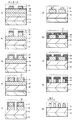
第1の実施の形態について説明する。図1(a)〜(j)は本実施形態に係る半導体装置の製造方法の工程を示す断面図である。なお、本実施形態および以下に示す実施形態においては、素子分離領域やゲート電極を加工する際のハードマスク、ダマシン構造の配線の溝形成などに使用することが可能なオルトケイ酸テトラエチル(以下、TEOSと略す)膜やシリコン窒化膜のラインアンドスペースパターン形成を行う際のハードマスクとなるアモルファスシリコン膜などのパターン形成を行う場合を説明するが、工程や材料を適宜使い分けることによって微細なパターン形成が必要な種々の膜に広く適用できることはいうまでもない。
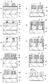
次に、第2の実施の形態について説明する。図4(a)〜(j)は本実施形態に係る半導体装置の製造方法の工程を示す断面図である。
次に、第3の実施の形態について説明する。図5(a)〜(f)は本実施形態に係る半導体装置の製造方法の工程を示す断面図である。
次に、第4の実施の形態について説明する。図6(a)〜(h)は本実施形態に係る半導体装置の製造方法の工程を示す断面図である。
次に、第5の実施の形態について説明する。図7(a)〜(e)は本実施形態に係る半導体装置の製造方法の工程を示す断面図である。
次に、第6の実施の形態について説明する。図8(a)〜(j)は本実施形態に係る半導体装置の製造方法の工程を示す断面図である。
Claims (2)
- パターニングすべき第1の膜上に、ラインとスペースの比率が1:1のパターンを有する膜を形成した後、ラインとスペースの比率が3:1となるように前記膜の両側に側壁を形成して、ラインとスペースの比率が3:1のパターンを形成する工程と、
前記ラインとスペースの比率が3:1のパターンをマスクとして前記第1の膜を加工する工程と、
前記第1の膜の加工後、前記ラインとスペースの比率が3:1のパターン両側の幅それぞれ1/3分を選択的に除去する工程と、
前記加工された第1の膜を、前記両側が除去されたパターン直下を除いて改質する工程と、
前記両側が除去されたパターンを除去する工程と、
前記第1の膜の非改質部分を選択的に除去して、ライン幅がリソグラフィの解像限界以下であるパターンを形成する工程と、
を含むことを特徴とする半導体装置の製造方法。 - パターニングすべき第1の膜上に少なくとも第2の膜を形成し、その上にラインとスペースの比率が1:1のパターンを有する第3の膜を形成した後、前記第3の膜をマスクとして前記第2の膜をテーパ加工してラインとスペースの比率が3:1のパターンを形成し、さらに、この第2の膜に形成されたパターンを前記パターニングすべき第1の膜まで転写する工程と、
前記第3の膜を除去する工程と、
前記第1の膜上に転写されたラインとスペースの比率が3:1のパターンを有する前記第2の膜の両側の幅それぞれ1/3分を選択的に除去する工程と、
前記第1の膜の露出した表面のみを酸化する工程と、
前記第2の膜を除去する工程と、
前記第1の膜の表面が酸化されていない部分を異方性エッチングにより除去して、ライン幅がリソグラフィの解像限界以下であるパターンを形成する工程と、
を含むことを特徴とする半導体装置の製造方法。
Priority Applications (2)
| Application Number | Priority Date | Filing Date | Title |
|---|---|---|---|
| JP2007233908A JP4621718B2 (ja) | 2007-09-10 | 2007-09-10 | 半導体装置の製造方法 |
| US12/208,010 US20090191712A1 (en) | 2007-09-10 | 2008-09-10 | Manufacturing method of semiconductor device |
Applications Claiming Priority (1)
| Application Number | Priority Date | Filing Date | Title |
|---|---|---|---|
| JP2007233908A JP4621718B2 (ja) | 2007-09-10 | 2007-09-10 | 半導体装置の製造方法 |
Publications (3)
| Publication Number | Publication Date |
|---|---|
| JP2009065093A JP2009065093A (ja) | 2009-03-26 |
| JP2009065093A5 JP2009065093A5 (ja) | 2009-10-22 |
| JP4621718B2 true JP4621718B2 (ja) | 2011-01-26 |
Family
ID=40559382
Family Applications (1)
| Application Number | Title | Priority Date | Filing Date |
|---|---|---|---|
| JP2007233908A Active JP4621718B2 (ja) | 2007-09-10 | 2007-09-10 | 半導体装置の製造方法 |
Country Status (2)
| Country | Link |
|---|---|
| US (1) | US20090191712A1 (ja) |
| JP (1) | JP4621718B2 (ja) |
Families Citing this family (2)
| Publication number | Priority date | Publication date | Assignee | Title |
|---|---|---|---|---|
| JP4901898B2 (ja) | 2009-03-30 | 2012-03-21 | 株式会社東芝 | 半導体装置の製造方法 |
| US9337197B1 (en) * | 2014-10-28 | 2016-05-10 | Globalfoundries Inc. | Semiconductor structure having FinFET ultra thin body and methods of fabrication thereof |
Citations (3)
| Publication number | Priority date | Publication date | Assignee | Title |
|---|---|---|---|---|
| JP2002280388A (ja) * | 2001-03-15 | 2002-09-27 | Toshiba Corp | 半導体装置の製造方法 |
| JP2004014652A (ja) * | 2002-06-04 | 2004-01-15 | Ricoh Co Ltd | 微細パターンの形成方法 |
| JP2007005377A (ja) * | 2005-06-21 | 2007-01-11 | Tokyo Electron Ltd | プラズマエッチング方法、制御プログラム、コンピュータ記憶媒体及びプラズマエッチング装置 |
Family Cites Families (6)
| Publication number | Priority date | Publication date | Assignee | Title |
|---|---|---|---|---|
| JPH0472622A (ja) * | 1990-07-13 | 1992-03-06 | Hitachi Ltd | 半導体装置およびその製造方法 |
| JPH08306698A (ja) * | 1995-05-10 | 1996-11-22 | Casio Comput Co Ltd | パターン形成方法 |
| DE10142590A1 (de) * | 2001-08-31 | 2003-04-03 | Infineon Technologies Ag | Verfahren zur Seitenwandverstärkung von Resiststrukturen und zur Herstellung von Strukturen mit reduzierter Strukturgröße |
| US6867116B1 (en) * | 2003-11-10 | 2005-03-15 | Macronix International Co., Ltd. | Fabrication method of sub-resolution pitch for integrated circuits |
| US7183205B2 (en) * | 2004-06-08 | 2007-02-27 | Macronix International Co., Ltd. | Method of pitch dimension shrinkage |
| US7465525B2 (en) * | 2005-05-10 | 2008-12-16 | Lam Research Corporation | Reticle alignment and overlay for multiple reticle process |
-
2007
- 2007-09-10 JP JP2007233908A patent/JP4621718B2/ja active Active
-
2008
- 2008-09-10 US US12/208,010 patent/US20090191712A1/en not_active Abandoned
Patent Citations (3)
| Publication number | Priority date | Publication date | Assignee | Title |
|---|---|---|---|---|
| JP2002280388A (ja) * | 2001-03-15 | 2002-09-27 | Toshiba Corp | 半導体装置の製造方法 |
| JP2004014652A (ja) * | 2002-06-04 | 2004-01-15 | Ricoh Co Ltd | 微細パターンの形成方法 |
| JP2007005377A (ja) * | 2005-06-21 | 2007-01-11 | Tokyo Electron Ltd | プラズマエッチング方法、制御プログラム、コンピュータ記憶媒体及びプラズマエッチング装置 |
Also Published As
| Publication number | Publication date |
|---|---|
| JP2009065093A (ja) | 2009-03-26 |
| US20090191712A1 (en) | 2009-07-30 |
Similar Documents
| Publication | Publication Date | Title |
|---|---|---|
| KR100640640B1 (ko) | 미세 피치의 하드마스크를 이용한 반도체 소자의 미세 패턴형성 방법 | |
| TWI356446B (en) | Methods to reduce the critical dimension of semico | |
| JP5122106B2 (ja) | 炭素含有膜エッチング方法及びこれを利用した半導体素子の製造方法 | |
| JP5492381B2 (ja) | ダブルパターニング工程を用いる半導体素子の微細パターン形成方法 | |
| JP2009152243A (ja) | 半導体装置の製造方法 | |
| US8222152B2 (en) | Method for fabricating hole pattern | |
| TWI390602B (zh) | 半導體裝置之製造方法 | |
| TWI335615B (en) | Method for fabricating semiconductor device using arf photolithography capable of protecting tapered profile of hard mask | |
| JP5100198B2 (ja) | 半導体素子の微細パターンの形成方法 | |
| JP2009071306A (ja) | 半導体素子の微細パターン形成方法 | |
| JP2009016813A (ja) | 微細パターンの形成方法 | |
| JPWO2007116515A1 (ja) | 半導体装置及びその製造方法、ドライエッチング方法、配線材料の作製方法、並びにエッチング装置 | |
| JP4621718B2 (ja) | 半導体装置の製造方法 | |
| TW200824002A (en) | Method for fabricating semiconductor device | |
| JP5164446B2 (ja) | 半導体素子の微細パターン形成方法 | |
| JP2009094379A (ja) | 半導体装置の製造方法 | |
| KR20070113604A (ko) | 반도체 소자의 미세패턴 형성방법 | |
| JP2008124399A (ja) | 半導体装置の製造方法 | |
| KR100912958B1 (ko) | 반도체 소자의 미세 패턴 제조 방법 | |
| JP2006032801A (ja) | 半導体装置の製造方法 | |
| KR20050068363A (ko) | 하드 마스크를 이용한 미세 패턴 형성 방법 | |
| JP4768732B2 (ja) | 半導体装置及びその製造方法、ドライエッチング方法、配線材料の作製方法、並びにエッチング装置 | |
| JP2002026020A (ja) | 半導体装置の製造方法 | |
| KR100626743B1 (ko) | 반도체 소자의 패턴 형성 방법 | |
| KR101103809B1 (ko) | 반도체 소자의 제조 방법 |
Legal Events
| Date | Code | Title | Description |
|---|---|---|---|
| A521 | Written amendment |
Free format text: JAPANESE INTERMEDIATE CODE: A523 Effective date: 20090909 |
|
| A621 | Written request for application examination |
Free format text: JAPANESE INTERMEDIATE CODE: A621 Effective date: 20090909 |
|
| A131 | Notification of reasons for refusal |
Free format text: JAPANESE INTERMEDIATE CODE: A131 Effective date: 20100316 |
|
| A521 | Written amendment |
Free format text: JAPANESE INTERMEDIATE CODE: A523 Effective date: 20100517 |
|
| RD02 | Notification of acceptance of power of attorney |
Free format text: JAPANESE INTERMEDIATE CODE: A7422 Effective date: 20100517 |
|
| A131 | Notification of reasons for refusal |
Free format text: JAPANESE INTERMEDIATE CODE: A131 Effective date: 20100706 |
|
| A521 | Written amendment |
Free format text: JAPANESE INTERMEDIATE CODE: A523 Effective date: 20100809 |
|
| TRDD | Decision of grant or rejection written | ||
| A01 | Written decision to grant a patent or to grant a registration (utility model) |
Free format text: JAPANESE INTERMEDIATE CODE: A01 Effective date: 20101005 |
|
| A01 | Written decision to grant a patent or to grant a registration (utility model) |
Free format text: JAPANESE INTERMEDIATE CODE: A01 |
|
| A61 | First payment of annual fees (during grant procedure) |
Free format text: JAPANESE INTERMEDIATE CODE: A61 Effective date: 20101101 |
|
| FPAY | Renewal fee payment (event date is renewal date of database) |
Free format text: PAYMENT UNTIL: 20131105 Year of fee payment: 3 |
|
| R151 | Written notification of patent or utility model registration |
Ref document number: 4621718 Country of ref document: JP Free format text: JAPANESE INTERMEDIATE CODE: R151 |
|
| FPAY | Renewal fee payment (event date is renewal date of database) |
Free format text: PAYMENT UNTIL: 20131105 Year of fee payment: 3 |
|
| S111 | Request for change of ownership or part of ownership |
Free format text: JAPANESE INTERMEDIATE CODE: R313111 |
|
| R350 | Written notification of registration of transfer |
Free format text: JAPANESE INTERMEDIATE CODE: R350 |
|
| S111 | Request for change of ownership or part of ownership |
Free format text: JAPANESE INTERMEDIATE CODE: R313111 |
|
| R350 | Written notification of registration of transfer |
Free format text: JAPANESE INTERMEDIATE CODE: R350 |