JP4618786B2 - 固体撮像装置の製造方法 - Google Patents
固体撮像装置の製造方法 Download PDFInfo
- Publication number
- JP4618786B2 JP4618786B2 JP2005021276A JP2005021276A JP4618786B2 JP 4618786 B2 JP4618786 B2 JP 4618786B2 JP 2005021276 A JP2005021276 A JP 2005021276A JP 2005021276 A JP2005021276 A JP 2005021276A JP 4618786 B2 JP4618786 B2 JP 4618786B2
- Authority
- JP
- Japan
- Prior art keywords
- film
- insulating film
- wiring
- imaging device
- state imaging
- Prior art date
- Legal status (The legal status is an assumption and is not a legal conclusion. Google has not performed a legal analysis and makes no representation as to the accuracy of the status listed.)
- Expired - Fee Related
Links
- 238000000034 method Methods 0.000 title claims description 54
- 238000003384 imaging method Methods 0.000 title claims description 40
- 238000004519 manufacturing process Methods 0.000 title claims description 25
- 229910052751 metal Inorganic materials 0.000 claims description 24
- 239000002184 metal Substances 0.000 claims description 24
- 238000002161 passivation Methods 0.000 claims description 22
- 239000000758 substrate Substances 0.000 claims description 22
- 238000005498 polishing Methods 0.000 claims description 18
- 229910052710 silicon Inorganic materials 0.000 claims description 12
- 239000010703 silicon Substances 0.000 claims description 12
- XUIMIQQOPSSXEZ-UHFFFAOYSA-N Silicon Chemical compound [Si] XUIMIQQOPSSXEZ-UHFFFAOYSA-N 0.000 claims description 11
- 229910052581 Si3N4 Inorganic materials 0.000 claims description 9
- 238000005229 chemical vapour deposition Methods 0.000 claims description 9
- HQVNEWCFYHHQES-UHFFFAOYSA-N silicon nitride Chemical compound N12[Si]34N5[Si]62N3[Si]51N64 HQVNEWCFYHHQES-UHFFFAOYSA-N 0.000 claims description 9
- 238000006243 chemical reaction Methods 0.000 claims description 7
- 238000000151 deposition Methods 0.000 claims description 6
- 238000001020 plasma etching Methods 0.000 claims description 6
- 230000008021 deposition Effects 0.000 claims description 3
- 239000000126 substance Substances 0.000 claims description 3
- WFKWXMTUELFFGS-UHFFFAOYSA-N tungsten Chemical compound [W] WFKWXMTUELFFGS-UHFFFAOYSA-N 0.000 description 22
- 229910052721 tungsten Inorganic materials 0.000 description 21
- 239000010937 tungsten Substances 0.000 description 21
- VYPSYNLAJGMNEJ-UHFFFAOYSA-N Silicium dioxide Chemical compound O=[Si]=O VYPSYNLAJGMNEJ-UHFFFAOYSA-N 0.000 description 7
- 238000000206 photolithography Methods 0.000 description 7
- 229910052814 silicon oxide Inorganic materials 0.000 description 7
- 238000005530 etching Methods 0.000 description 6
- 230000000149 penetrating effect Effects 0.000 description 6
- 230000035945 sensitivity Effects 0.000 description 6
- 238000003860 storage Methods 0.000 description 6
- 238000009826 distribution Methods 0.000 description 5
- 239000001257 hydrogen Substances 0.000 description 5
- 229910052739 hydrogen Inorganic materials 0.000 description 5
- 238000005268 plasma chemical vapour deposition Methods 0.000 description 5
- UFHFLCQGNIYNRP-UHFFFAOYSA-N Hydrogen Chemical compound [H][H] UFHFLCQGNIYNRP-UHFFFAOYSA-N 0.000 description 4
- 229910052782 aluminium Inorganic materials 0.000 description 4
- XAGFODPZIPBFFR-UHFFFAOYSA-N aluminium Chemical compound [Al] XAGFODPZIPBFFR-UHFFFAOYSA-N 0.000 description 4
- 238000005240 physical vapour deposition Methods 0.000 description 4
- 239000004065 semiconductor Substances 0.000 description 4
- 238000009792 diffusion process Methods 0.000 description 3
- 239000007789 gas Substances 0.000 description 3
- 230000003321 amplification Effects 0.000 description 2
- 230000015572 biosynthetic process Effects 0.000 description 2
- 239000003086 colorant Substances 0.000 description 2
- 230000006866 deterioration Effects 0.000 description 2
- 239000012535 impurity Substances 0.000 description 2
- 238000003199 nucleic acid amplification method Methods 0.000 description 2
- 230000002093 peripheral effect Effects 0.000 description 2
- 230000003595 spectral effect Effects 0.000 description 2
- 206010034960 Photophobia Diseases 0.000 description 1
- 238000009825 accumulation Methods 0.000 description 1
- 229910002065 alloy metal Inorganic materials 0.000 description 1
- 238000010586 diagram Methods 0.000 description 1
- 150000002431 hydrogen Chemical class 0.000 description 1
- 238000009413 insulation Methods 0.000 description 1
- 208000013469 light sensitivity Diseases 0.000 description 1
- 239000002994 raw material Substances 0.000 description 1
- 239000003870 refractory metal Substances 0.000 description 1
- 150000003376 silicon Chemical class 0.000 description 1
- 238000002230 thermal chemical vapour deposition Methods 0.000 description 1
- NXHILIPIEUBEPD-UHFFFAOYSA-H tungsten hexafluoride Chemical compound F[W](F)(F)(F)(F)F NXHILIPIEUBEPD-UHFFFAOYSA-H 0.000 description 1
Images


Classifications
-
- H—ELECTRICITY
- H01—ELECTRIC ELEMENTS
- H01L—SEMICONDUCTOR DEVICES NOT COVERED BY CLASS H10
- H01L27/00—Devices consisting of a plurality of semiconductor or other solid-state components formed in or on a common substrate
- H01L27/14—Devices consisting of a plurality of semiconductor or other solid-state components formed in or on a common substrate including semiconductor components sensitive to infrared radiation, light, electromagnetic radiation of shorter wavelength or corpuscular radiation and specially adapted either for the conversion of the energy of such radiation into electrical energy or for the control of electrical energy by such radiation
- H01L27/144—Devices controlled by radiation
- H01L27/146—Imager structures
- H01L27/14643—Photodiode arrays; MOS imagers
-
- H—ELECTRICITY
- H01—ELECTRIC ELEMENTS
- H01L—SEMICONDUCTOR DEVICES NOT COVERED BY CLASS H10
- H01L27/00—Devices consisting of a plurality of semiconductor or other solid-state components formed in or on a common substrate
- H01L27/14—Devices consisting of a plurality of semiconductor or other solid-state components formed in or on a common substrate including semiconductor components sensitive to infrared radiation, light, electromagnetic radiation of shorter wavelength or corpuscular radiation and specially adapted either for the conversion of the energy of such radiation into electrical energy or for the control of electrical energy by such radiation
- H01L27/144—Devices controlled by radiation
- H01L27/146—Imager structures
- H01L27/14601—Structural or functional details thereof
- H01L27/1462—Coatings
-
- H—ELECTRICITY
- H01—ELECTRIC ELEMENTS
- H01L—SEMICONDUCTOR DEVICES NOT COVERED BY CLASS H10
- H01L27/00—Devices consisting of a plurality of semiconductor or other solid-state components formed in or on a common substrate
- H01L27/14—Devices consisting of a plurality of semiconductor or other solid-state components formed in or on a common substrate including semiconductor components sensitive to infrared radiation, light, electromagnetic radiation of shorter wavelength or corpuscular radiation and specially adapted either for the conversion of the energy of such radiation into electrical energy or for the control of electrical energy by such radiation
- H01L27/144—Devices controlled by radiation
- H01L27/146—Imager structures
- H01L27/14601—Structural or functional details thereof
- H01L27/14625—Optical elements or arrangements associated with the device
- H01L27/14627—Microlenses
-
- H—ELECTRICITY
- H01—ELECTRIC ELEMENTS
- H01L—SEMICONDUCTOR DEVICES NOT COVERED BY CLASS H10
- H01L27/00—Devices consisting of a plurality of semiconductor or other solid-state components formed in or on a common substrate
- H01L27/14—Devices consisting of a plurality of semiconductor or other solid-state components formed in or on a common substrate including semiconductor components sensitive to infrared radiation, light, electromagnetic radiation of shorter wavelength or corpuscular radiation and specially adapted either for the conversion of the energy of such radiation into electrical energy or for the control of electrical energy by such radiation
- H01L27/144—Devices controlled by radiation
- H01L27/146—Imager structures
- H01L27/14601—Structural or functional details thereof
- H01L27/14636—Interconnect structures
-
- H—ELECTRICITY
- H01—ELECTRIC ELEMENTS
- H01L—SEMICONDUCTOR DEVICES NOT COVERED BY CLASS H10
- H01L27/00—Devices consisting of a plurality of semiconductor or other solid-state components formed in or on a common substrate
- H01L27/14—Devices consisting of a plurality of semiconductor or other solid-state components formed in or on a common substrate including semiconductor components sensitive to infrared radiation, light, electromagnetic radiation of shorter wavelength or corpuscular radiation and specially adapted either for the conversion of the energy of such radiation into electrical energy or for the control of electrical energy by such radiation
- H01L27/144—Devices controlled by radiation
- H01L27/146—Imager structures
- H01L27/14683—Processes or apparatus peculiar to the manufacture or treatment of these devices or parts thereof
- H01L27/14685—Process for coatings or optical elements
-
- H—ELECTRICITY
- H01—ELECTRIC ELEMENTS
- H01L—SEMICONDUCTOR DEVICES NOT COVERED BY CLASS H10
- H01L27/00—Devices consisting of a plurality of semiconductor or other solid-state components formed in or on a common substrate
- H01L27/14—Devices consisting of a plurality of semiconductor or other solid-state components formed in or on a common substrate including semiconductor components sensitive to infrared radiation, light, electromagnetic radiation of shorter wavelength or corpuscular radiation and specially adapted either for the conversion of the energy of such radiation into electrical energy or for the control of electrical energy by such radiation
- H01L27/144—Devices controlled by radiation
- H01L27/146—Imager structures
- H01L27/14683—Processes or apparatus peculiar to the manufacture or treatment of these devices or parts thereof
- H01L27/14689—MOS based technologies
Description
以下、本発明の固体撮像装置の製造方法に係る固体撮像装置の基本構造について説明する。図1には、単位素子の要部断面模式図を示す。固体撮像装置の一例としてCMOSエリアセンサを例に説明する。ここで、CMOSエリアセンサとは、撮像領域と周辺回路領域を略同一のプロセス(CMOSプロセス)で形成するセンサを指す。CMOSエリアセンサ10は、基板103に形成された光電変換素子であるフォトダイオード100と、光電変換素子からの電気信号を転送する転送MOSトランジスタ101と、転送MOSトランジスタ101等のMOSトランジスタの駆動用バイアスを与えるための配線、光電変換された電荷を周辺の信号処理回路へ転送するための配線、所望の電圧を供給するための電源配線、遮光を行なうための配線等を含む配線部102とを有している。また、画素に増幅機能を備える場合には、転送MOSトランジスタの他に、増幅用MOSトランジスタ、リセット用MOSトランジスタ、画素選択用MOSトランジスタ等を必要に応じて有している。フォトダイオード100と転送MOSトランジスタ101は、CMOSエリアセンサ10の撮像領域を形成している。N型シリコン基板103にはP型ウエル104が形成されている。P型ウエル104上に、N型電荷蓄積領域108が形成され、その上には、フォトダイオードを埋め込み構造とするための表面P型領域109が形成されている。また、転送MOSトランジスタのゲート電極107を介して、N型電荷蓄積領域108の反対側に転送MOSトランジスタ101のドレイン領域110が形成されている。N型不純物領域であるドレイン領域110は、転送された電荷を保持し、電圧に変換して出力するフローティングディフュージョンとしても機能する。他の単位素子との間はフィールド酸化膜105で分離されている。
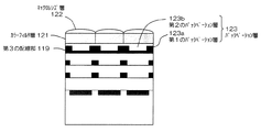
続いて、本発明の第2の実施形態に係る固体撮像装置の製造方法について説明する。図3には本実施形態に係るCMOSエリアセンサの単位素子の要部断面模式図を示す。本実施形態は、二層構造のパッシベーション膜123を形成することを特徴としている。基板103から第3の配線部119までの構造は、第1の実施形態に係るCMOSエリアセンサと同様である。パッシベーション膜123は、反射防止膜となる酸窒化シリコン膜からなる第1のパッシベーション膜123a上に、窒化シリコン膜からなる第2のパッシベーション膜123bが形成された二層構造である。
100 フォトダイオード部
101 MOSトランジスタ部
102 配線部
103 N型シリコン基板
104 P型ウエル
111 第1の絶縁膜
112 コンタクトプラグ
113 第1の配線部
114 第2の絶縁膜
115 ビアプラグ
116 第2の配線部
117 第3の絶縁膜
118 ビアプラグ
119 第3の配線部
131,133,135 接続孔
132,134,136 タングステン膜
Claims (8)
- 基板と、
前記基板に形成された、光電変換素子と、該光電変換素子からの電気信号を転送する手段とを有する撮像領域と、
前記撮像領域の上に、積層方向に互いに異なる高さに設けられた複数の配線部と、
積層方向に隣接する前記配線部同士の間、および前記撮像領域と該撮像領域に積層方向に隣接する前記配線部との間に設けられた複数の絶縁膜と、
各々が前記絶縁膜のひとつを貫通して設けられ、積層方向に隣接する前記配線部同士、または前記配線部と前記撮像領域の一部とを電気的に導通させる、複数の埋込プラグと、
を有する固体撮像装置の製造方法において、
前記埋込プラグを形成する工程は、
前記埋込プラグが形成される前記絶縁膜に接続孔を形成する工程と、
前記接続孔が形成された前記絶縁膜に、該接続孔の内部、および該絶縁膜の積層方向上面の少なくとも一部を覆うように金属膜を堆積させる金属膜堆積工程と、
前記堆積された金属膜を研磨して前記接続孔の内部を除く該金属膜を除去すると同時に前記絶縁膜を平坦化する金属膜除去工程とを有し、
前記金属膜除去工程は、積層方向最上部の前記埋込プラグについてはエッチバック法を用い、
他の前記埋込プラグについては化学的機械研磨法を用いることを特徴とする、固体撮像装置の製造方法。 - 前記積層方向最上部の前記埋込プラグを形成する工程は、前記金属膜堆積工程では化学気相成長法を用いる、請求項1に記載の固体撮像装置の製造方法。
- 前記積層方向最上部の前記絶縁膜の上部にパッシベーション層を設ける工程を有する、請求項1または2に記載の固体撮像装置の製造方法。
- 前記パッシベーション膜は、窒化シリコン膜である、請求項3に記載の固体撮像装置の製造方法。
- 前記パッシベーション膜と前記積層方向最上部の前記絶縁膜との間に、該パッシベーション膜と前記積層方向最上部の前記絶縁膜との界面における反射を低減する反射防止膜を形成する工程を有する、請求項4に記載の固体撮像装置の製造方法。
- 前記反射防止膜は酸窒化シリコン膜である、請求項5に記載の固体撮像装置の製造方法。
- 前記エッチバック法は、反応性イオンエッチング法である、請求項1から6のいずれか1項に記載の固体撮像装置の製造方法。
- 前記積層方向最上部の前記配線部は遮光配線として機能する、請求項1から7のいずれか1項に記載の固体撮像装置の製造方法。
Priority Applications (2)
| Application Number | Priority Date | Filing Date | Title |
|---|---|---|---|
| JP2005021276A JP4618786B2 (ja) | 2005-01-28 | 2005-01-28 | 固体撮像装置の製造方法 |
| US11/275,672 US7393715B2 (en) | 2005-01-28 | 2006-01-24 | Manufacturing method for image pickup apparatus |
Applications Claiming Priority (1)
| Application Number | Priority Date | Filing Date | Title |
|---|---|---|---|
| JP2005021276A JP4618786B2 (ja) | 2005-01-28 | 2005-01-28 | 固体撮像装置の製造方法 |
Publications (3)
| Publication Number | Publication Date |
|---|---|
| JP2006210685A JP2006210685A (ja) | 2006-08-10 |
| JP2006210685A5 JP2006210685A5 (ja) | 2008-02-14 |
| JP4618786B2 true JP4618786B2 (ja) | 2011-01-26 |
Family
ID=36757094
Family Applications (1)
| Application Number | Title | Priority Date | Filing Date |
|---|---|---|---|
| JP2005021276A Expired - Fee Related JP4618786B2 (ja) | 2005-01-28 | 2005-01-28 | 固体撮像装置の製造方法 |
Country Status (2)
| Country | Link |
|---|---|
| US (1) | US7393715B2 (ja) |
| JP (1) | JP4618786B2 (ja) |
Families Citing this family (22)
| Publication number | Priority date | Publication date | Assignee | Title |
|---|---|---|---|---|
| JP4646577B2 (ja) | 2004-09-01 | 2011-03-09 | キヤノン株式会社 | 光電変換装置、その製造方法及び撮像システム |
| US7592645B2 (en) * | 2004-12-08 | 2009-09-22 | Canon Kabushiki Kaisha | Photoelectric conversion device and method for producing photoelectric conversion device |
| JP2006237315A (ja) * | 2005-02-25 | 2006-09-07 | Matsushita Electric Ind Co Ltd | 固体撮像装置 |
| US7884434B2 (en) * | 2005-12-19 | 2011-02-08 | Canon Kabushiki Kaisha | Photoelectric conversion apparatus, producing method therefor, image pickup module and image pickup system |
| JP5305622B2 (ja) * | 2006-08-31 | 2013-10-02 | キヤノン株式会社 | 光電変換装置の製造方法 |
| JP4137161B1 (ja) | 2007-02-23 | 2008-08-20 | キヤノン株式会社 | 光電変換装置の製造方法 |
| JP4110192B1 (ja) * | 2007-02-23 | 2008-07-02 | キヤノン株式会社 | 光電変換装置及び光電変換装置を用いた撮像システム |
| JP5059476B2 (ja) * | 2007-04-23 | 2012-10-24 | ラピスセミコンダクタ株式会社 | 半導体装置、光測定装置、光検出装置、及び半導体装置の製造方法 |
| KR100881200B1 (ko) * | 2007-07-30 | 2009-02-05 | 삼성전자주식회사 | 씨모스 이미지 센서 및 그 제조방법 |
| JP2009043772A (ja) * | 2007-08-06 | 2009-02-26 | Panasonic Corp | 固体撮像装置及びその製造方法 |
| KR100922929B1 (ko) * | 2007-12-28 | 2009-10-22 | 주식회사 동부하이텍 | 이미지센서 및 그 제조방법 |
| JP5288823B2 (ja) * | 2008-02-18 | 2013-09-11 | キヤノン株式会社 | 光電変換装置、及び光電変換装置の製造方法 |
| JP5314914B2 (ja) * | 2008-04-04 | 2013-10-16 | キヤノン株式会社 | 光電変換装置、撮像システム、設計方法、及び光電変換装置の製造方法 |
| KR101045716B1 (ko) * | 2008-07-29 | 2011-06-30 | 주식회사 동부하이텍 | 이미지센서 및 그 제조방법 |
| JP2010073819A (ja) * | 2008-09-17 | 2010-04-02 | Canon Inc | 光電変換装置及び撮像システム |
| KR20100074966A (ko) * | 2008-12-24 | 2010-07-02 | 삼성전자주식회사 | 브리지 방지 금속 배선 구조를 갖는 시모스 이미지 센서 및제조 방법 |
| US8441052B2 (en) * | 2009-10-21 | 2013-05-14 | Hiok Nam Tay | Color-optimized image sensor |
| JP5704811B2 (ja) * | 2009-12-11 | 2015-04-22 | キヤノン株式会社 | 固体撮像装置の製造方法 |
| JP6230343B2 (ja) | 2013-09-06 | 2017-11-15 | キヤノン株式会社 | 固体撮像装置、その駆動方法及び撮像システム |
| JP2015144248A (ja) * | 2013-12-25 | 2015-08-06 | キヤノン株式会社 | 半導体装置、及びその製造方法 |
| JP2018082295A (ja) | 2016-11-16 | 2018-05-24 | キヤノン株式会社 | 撮像装置及び撮像システム |
| JP2021019058A (ja) | 2019-07-18 | 2021-02-15 | キヤノン株式会社 | 光電変換装置および機器 |
Citations (6)
| Publication number | Priority date | Publication date | Assignee | Title |
|---|---|---|---|---|
| JP2003204055A (ja) * | 2002-01-09 | 2003-07-18 | Sony Corp | 固体撮像装置およびその製造方法 |
| JP2003224249A (ja) * | 2002-01-28 | 2003-08-08 | Sony Corp | 半導体撮像装置及びその製造方法 |
| JP2004031918A (ja) * | 2002-04-12 | 2004-01-29 | Hitachi Ltd | 半導体装置 |
| JP2004165236A (ja) * | 2002-11-11 | 2004-06-10 | Sony Corp | 固体撮像装置の製造方法 |
| JP2004221527A (ja) * | 2003-01-16 | 2004-08-05 | Samsung Electronics Co Ltd | イメージ素子及びその製造方法 |
| JP2004281911A (ja) * | 2003-03-18 | 2004-10-07 | Sony Corp | 固体撮像装置及びその製造方法 |
Family Cites Families (16)
| Publication number | Priority date | Publication date | Assignee | Title |
|---|---|---|---|---|
| CA1270058C (en) * | 1984-12-28 | 1990-06-05 | CAMERA | |
| US4731685A (en) * | 1985-10-16 | 1988-03-15 | Ampex Corporation | Transducing head mounting on an unsupported length of spring |
| DE3856165T2 (de) * | 1987-01-29 | 1998-08-27 | Canon Kk | Photovoltaischer Wandler |
| US4959723A (en) * | 1987-11-06 | 1990-09-25 | Canon Kabushiki Kaisha | Solid state image pickup apparatus having multi-phase scanning pulse to read out accumulated signal |
| US5146339A (en) * | 1989-11-21 | 1992-09-08 | Canon Kabushiki Kaisha | Photoelectric converting apparatus employing Darlington transistor readout |
| CA2056087C (en) * | 1990-11-27 | 1998-01-27 | Masakazu Morishita | Photoelectric converting device and information processing apparatus employing the same |
| JP2000228509A (ja) * | 1999-02-05 | 2000-08-15 | Fujitsu Ltd | 半導体装置 |
| US6114243A (en) * | 1999-11-15 | 2000-09-05 | Chartered Semiconductor Manufacturing Ltd | Method to avoid copper contamination on the sidewall of a via or a dual damascene structure |
| JP3542545B2 (ja) | 2000-06-08 | 2004-07-14 | キヤノン株式会社 | 固体撮像装置 |
| JP2002231915A (ja) | 2001-01-31 | 2002-08-16 | Sony Corp | 固体撮像素子 |
| JP3840214B2 (ja) * | 2003-01-06 | 2006-11-01 | キヤノン株式会社 | 光電変換装置及び光電変換装置の製造方法及び同光電変換装置を用いたカメラ |
| JP4256347B2 (ja) * | 2003-04-30 | 2009-04-22 | 富士通マイクロエレクトロニクス株式会社 | 半導体装置の製造方法 |
| JP4383959B2 (ja) * | 2003-05-28 | 2009-12-16 | キヤノン株式会社 | 光電変換装置およびその製造方法 |
| JP4646577B2 (ja) * | 2004-09-01 | 2011-03-09 | キヤノン株式会社 | 光電変換装置、その製造方法及び撮像システム |
| US7592645B2 (en) * | 2004-12-08 | 2009-09-22 | Canon Kabushiki Kaisha | Photoelectric conversion device and method for producing photoelectric conversion device |
| JP2006261597A (ja) * | 2005-03-18 | 2006-09-28 | Canon Inc | 固体撮像装置、その製造方法及びカメラ |
-
2005
- 2005-01-28 JP JP2005021276A patent/JP4618786B2/ja not_active Expired - Fee Related
-
2006
- 2006-01-24 US US11/275,672 patent/US7393715B2/en not_active Expired - Fee Related
Patent Citations (6)
| Publication number | Priority date | Publication date | Assignee | Title |
|---|---|---|---|---|
| JP2003204055A (ja) * | 2002-01-09 | 2003-07-18 | Sony Corp | 固体撮像装置およびその製造方法 |
| JP2003224249A (ja) * | 2002-01-28 | 2003-08-08 | Sony Corp | 半導体撮像装置及びその製造方法 |
| JP2004031918A (ja) * | 2002-04-12 | 2004-01-29 | Hitachi Ltd | 半導体装置 |
| JP2004165236A (ja) * | 2002-11-11 | 2004-06-10 | Sony Corp | 固体撮像装置の製造方法 |
| JP2004221527A (ja) * | 2003-01-16 | 2004-08-05 | Samsung Electronics Co Ltd | イメージ素子及びその製造方法 |
| JP2004281911A (ja) * | 2003-03-18 | 2004-10-07 | Sony Corp | 固体撮像装置及びその製造方法 |
Also Published As
| Publication number | Publication date |
|---|---|
| US7393715B2 (en) | 2008-07-01 |
| JP2006210685A (ja) | 2006-08-10 |
| US20060172450A1 (en) | 2006-08-03 |
Similar Documents
| Publication | Publication Date | Title |
|---|---|---|
| JP4618786B2 (ja) | 固体撮像装置の製造方法 | |
| USRE46123E1 (en) | Solid-state image sensor and method of manufacturing the same | |
| TWI599025B (zh) | 半導體影像感測元件與其形成方法 | |
| JP5357441B2 (ja) | 固体撮像装置の製造方法 | |
| JP6061544B2 (ja) | 撮像装置の製造方法 | |
| US10134790B1 (en) | Image sensor and fabrication method therefor | |
| JP2016033972A (ja) | 撮像装置及び撮像システム | |
| JP2007048893A (ja) | 固体撮像素子およびその製造方法 | |
| JP5284438B2 (ja) | 固体撮像装置、及び固体撮像装置の製造方法 | |
| JP2009295918A (ja) | 固体撮像装置及びその製造方法 | |
| US20110159632A1 (en) | Method for manufacturing a solid-state image capturing element | |
| CN105826331B (zh) | 采用背面深沟槽隔离的背照式图像传感器的制作方法 | |
| US7462520B2 (en) | Methods of fabricating an image sensor | |
| US20090090989A1 (en) | Image Sensor and Method of Manufacturing the Same | |
| JP2006049834A (ja) | 固体撮像素子およびその製造方法 | |
| US8053268B2 (en) | Semiconductor device and method of manufacturing the same | |
| US7846761B2 (en) | Image sensor and method for manufacturing the same | |
| US20080054387A1 (en) | Image Sensor and Method for Manufacturing the Same | |
| KR20010061343A (ko) | 이미지센서 제조 방법 | |
| JP2010118661A (ja) | イメージセンサー及び前記イメージセンサーの製造方法 | |
| CN111916466A (zh) | 图像传感器及其形成方法 | |
| US20230136919A1 (en) | Image sensor and method of fabricating the same | |
| JP4705791B2 (ja) | 固体撮像素子の製造方法 | |
| JP2006351788A (ja) | 固体撮像素子およびその製造方法 | |
| US20220223634A1 (en) | Composite deep trench isolation structure in an image sensor |
Legal Events
| Date | Code | Title | Description |
|---|---|---|---|
| A521 | Request for written amendment filed |
Free format text: JAPANESE INTERMEDIATE CODE: A523 Effective date: 20071225 |
|
| A621 | Written request for application examination |
Free format text: JAPANESE INTERMEDIATE CODE: A621 Effective date: 20071225 |
|
| A131 | Notification of reasons for refusal |
Free format text: JAPANESE INTERMEDIATE CODE: A131 Effective date: 20100721 |
|
| A977 | Report on retrieval |
Free format text: JAPANESE INTERMEDIATE CODE: A971007 Effective date: 20100722 |
|
| A521 | Request for written amendment filed |
Free format text: JAPANESE INTERMEDIATE CODE: A523 Effective date: 20100921 |
|
| TRDD | Decision of grant or rejection written | ||
| A01 | Written decision to grant a patent or to grant a registration (utility model) |
Free format text: JAPANESE INTERMEDIATE CODE: A01 Effective date: 20101020 |
|
| A01 | Written decision to grant a patent or to grant a registration (utility model) |
Free format text: JAPANESE INTERMEDIATE CODE: A01 |
|
| A61 | First payment of annual fees (during grant procedure) |
Free format text: JAPANESE INTERMEDIATE CODE: A61 Effective date: 20101025 |
|
| FPAY | Renewal fee payment (event date is renewal date of database) |
Free format text: PAYMENT UNTIL: 20131105 Year of fee payment: 3 |
|
| R150 | Certificate of patent or registration of utility model |
Ref document number: 4618786 Country of ref document: JP Free format text: JAPANESE INTERMEDIATE CODE: R150 |
|
| LAPS | Cancellation because of no payment of annual fees |