JP4528626B2 - ボールグリッドアレイテンプレートを充填する装置及び方法 - Google Patents
ボールグリッドアレイテンプレートを充填する装置及び方法 Download PDFInfo
- Publication number
- JP4528626B2 JP4528626B2 JP2004545151A JP2004545151A JP4528626B2 JP 4528626 B2 JP4528626 B2 JP 4528626B2 JP 2004545151 A JP2004545151 A JP 2004545151A JP 2004545151 A JP2004545151 A JP 2004545151A JP 4528626 B2 JP4528626 B2 JP 4528626B2
- Authority
- JP
- Japan
- Prior art keywords
- ball
- base plate
- grid array
- solder
- ball grid
- Prior art date
- Legal status (The legal status is an assumption and is not a legal conclusion. Google has not performed a legal analysis and makes no representation as to the accuracy of the status listed.)
- Expired - Lifetime
Links
- 238000000034 method Methods 0.000 title claims description 25
- 229910000679 solder Inorganic materials 0.000 claims description 107
- 238000001514 detection method Methods 0.000 claims description 3
- 238000004891 communication Methods 0.000 claims description 2
- 230000004907 flux Effects 0.000 description 5
- 239000000758 substrate Substances 0.000 description 5
- 238000011109 contamination Methods 0.000 description 3
- 238000010586 diagram Methods 0.000 description 2
- 230000000284 resting effect Effects 0.000 description 2
- 230000003068 static effect Effects 0.000 description 2
- 238000012546 transfer Methods 0.000 description 2
- 230000002159 abnormal effect Effects 0.000 description 1
- 238000007796 conventional method Methods 0.000 description 1
- 238000000151 deposition Methods 0.000 description 1
- 238000013461 design Methods 0.000 description 1
- 238000005516 engineering process Methods 0.000 description 1
- 230000005484 gravity Effects 0.000 description 1
- 239000007788 liquid Substances 0.000 description 1
- 238000012544 monitoring process Methods 0.000 description 1
- 238000010408 sweeping Methods 0.000 description 1
Images


Classifications
-
- B—PERFORMING OPERATIONS; TRANSPORTING
- B23—MACHINE TOOLS; METAL-WORKING NOT OTHERWISE PROVIDED FOR
- B23K—SOLDERING OR UNSOLDERING; WELDING; CLADDING OR PLATING BY SOLDERING OR WELDING; CUTTING BY APPLYING HEAT LOCALLY, e.g. FLAME CUTTING; WORKING BY LASER BEAM
- B23K1/00—Soldering, e.g. brazing, or unsoldering
- B23K1/0008—Soldering, e.g. brazing, or unsoldering specially adapted for particular articles or work
- B23K1/0016—Brazing of electronic components
-
- B—PERFORMING OPERATIONS; TRANSPORTING
- B23—MACHINE TOOLS; METAL-WORKING NOT OTHERWISE PROVIDED FOR
- B23K—SOLDERING OR UNSOLDERING; WELDING; CLADDING OR PLATING BY SOLDERING OR WELDING; CUTTING BY APPLYING HEAT LOCALLY, e.g. FLAME CUTTING; WORKING BY LASER BEAM
- B23K3/00—Tools, devices, or special appurtenances for soldering, e.g. brazing, or unsoldering, not specially adapted for particular methods
- B23K3/06—Solder feeding devices; Solder melting pans
- B23K3/0607—Solder feeding devices
- B23K3/0623—Solder feeding devices for shaped solder piece feeding, e.g. preforms, bumps, balls, pellets, droplets
-
- H—ELECTRICITY
- H01—ELECTRIC ELEMENTS
- H01L—SEMICONDUCTOR DEVICES NOT COVERED BY CLASS H10
- H01L21/00—Processes or apparatus adapted for the manufacture or treatment of semiconductor or solid state devices or of parts thereof
- H01L21/02—Manufacture or treatment of semiconductor devices or of parts thereof
- H01L21/04—Manufacture or treatment of semiconductor devices or of parts thereof the devices having at least one potential-jump barrier or surface barrier, e.g. PN junction, depletion layer or carrier concentration layer
- H01L21/48—Manufacture or treatment of parts, e.g. containers, prior to assembly of the devices, using processes not provided for in a single one of the subgroups H01L21/06 - H01L21/326
- H01L21/4814—Conductive parts
- H01L21/4846—Leads on or in insulating or insulated substrates, e.g. metallisation
- H01L21/4853—Connection or disconnection of other leads to or from a metallisation, e.g. pins, wires, bumps
-
- H—ELECTRICITY
- H01—ELECTRIC ELEMENTS
- H01L—SEMICONDUCTOR DEVICES NOT COVERED BY CLASS H10
- H01L24/00—Arrangements for connecting or disconnecting semiconductor or solid-state bodies; Methods or apparatus related thereto
- H01L24/01—Means for bonding being attached to, or being formed on, the surface to be connected, e.g. chip-to-package, die-attach, "first-level" interconnects; Manufacturing methods related thereto
- H01L24/10—Bump connectors ; Manufacturing methods related thereto
- H01L24/11—Manufacturing methods
-
- B—PERFORMING OPERATIONS; TRANSPORTING
- B23—MACHINE TOOLS; METAL-WORKING NOT OTHERWISE PROVIDED FOR
- B23K—SOLDERING OR UNSOLDERING; WELDING; CLADDING OR PLATING BY SOLDERING OR WELDING; CUTTING BY APPLYING HEAT LOCALLY, e.g. FLAME CUTTING; WORKING BY LASER BEAM
- B23K2101/00—Articles made by soldering, welding or cutting
- B23K2101/36—Electric or electronic devices
- B23K2101/40—Semiconductor devices
-
- H—ELECTRICITY
- H01—ELECTRIC ELEMENTS
- H01L—SEMICONDUCTOR DEVICES NOT COVERED BY CLASS H10
- H01L2224/00—Indexing scheme for arrangements for connecting or disconnecting semiconductor or solid-state bodies and methods related thereto as covered by H01L24/00
- H01L2224/01—Means for bonding being attached to, or being formed on, the surface to be connected, e.g. chip-to-package, die-attach, "first-level" interconnects; Manufacturing methods related thereto
- H01L2224/10—Bump connectors; Manufacturing methods related thereto
- H01L2224/12—Structure, shape, material or disposition of the bump connectors prior to the connecting process
- H01L2224/13—Structure, shape, material or disposition of the bump connectors prior to the connecting process of an individual bump connector
- H01L2224/13001—Core members of the bump connector
- H01L2224/13099—Material
-
- H—ELECTRICITY
- H01—ELECTRIC ELEMENTS
- H01L—SEMICONDUCTOR DEVICES NOT COVERED BY CLASS H10
- H01L2924/00—Indexing scheme for arrangements or methods for connecting or disconnecting semiconductor or solid-state bodies as covered by H01L24/00
- H01L2924/01—Chemical elements
- H01L2924/01005—Boron [B]
-
- H—ELECTRICITY
- H01—ELECTRIC ELEMENTS
- H01L—SEMICONDUCTOR DEVICES NOT COVERED BY CLASS H10
- H01L2924/00—Indexing scheme for arrangements or methods for connecting or disconnecting semiconductor or solid-state bodies as covered by H01L24/00
- H01L2924/01—Chemical elements
- H01L2924/01006—Carbon [C]
-
- H—ELECTRICITY
- H01—ELECTRIC ELEMENTS
- H01L—SEMICONDUCTOR DEVICES NOT COVERED BY CLASS H10
- H01L2924/00—Indexing scheme for arrangements or methods for connecting or disconnecting semiconductor or solid-state bodies as covered by H01L24/00
- H01L2924/01—Chemical elements
- H01L2924/01027—Cobalt [Co]
-
- H—ELECTRICITY
- H01—ELECTRIC ELEMENTS
- H01L—SEMICONDUCTOR DEVICES NOT COVERED BY CLASS H10
- H01L2924/00—Indexing scheme for arrangements or methods for connecting or disconnecting semiconductor or solid-state bodies as covered by H01L24/00
- H01L2924/01—Chemical elements
- H01L2924/01033—Arsenic [As]
-
- H—ELECTRICITY
- H01—ELECTRIC ELEMENTS
- H01L—SEMICONDUCTOR DEVICES NOT COVERED BY CLASS H10
- H01L2924/00—Indexing scheme for arrangements or methods for connecting or disconnecting semiconductor or solid-state bodies as covered by H01L24/00
- H01L2924/01—Chemical elements
- H01L2924/01079—Gold [Au]
-
- H—ELECTRICITY
- H01—ELECTRIC ELEMENTS
- H01L—SEMICONDUCTOR DEVICES NOT COVERED BY CLASS H10
- H01L2924/00—Indexing scheme for arrangements or methods for connecting or disconnecting semiconductor or solid-state bodies as covered by H01L24/00
- H01L2924/01—Chemical elements
- H01L2924/01082—Lead [Pb]
-
- H—ELECTRICITY
- H01—ELECTRIC ELEMENTS
- H01L—SEMICONDUCTOR DEVICES NOT COVERED BY CLASS H10
- H01L2924/00—Indexing scheme for arrangements or methods for connecting or disconnecting semiconductor or solid-state bodies as covered by H01L24/00
- H01L2924/013—Alloys
- H01L2924/014—Solder alloys
-
- H—ELECTRICITY
- H05—ELECTRIC TECHNIQUES NOT OTHERWISE PROVIDED FOR
- H05K—PRINTED CIRCUITS; CASINGS OR CONSTRUCTIONAL DETAILS OF ELECTRIC APPARATUS; MANUFACTURE OF ASSEMBLAGES OF ELECTRICAL COMPONENTS
- H05K3/00—Apparatus or processes for manufacturing printed circuits
- H05K3/30—Assembling printed circuits with electric components, e.g. with resistor
- H05K3/32—Assembling printed circuits with electric components, e.g. with resistor electrically connecting electric components or wires to printed circuits
- H05K3/34—Assembling printed circuits with electric components, e.g. with resistor electrically connecting electric components or wires to printed circuits by soldering
- H05K3/3457—Solder materials or compositions; Methods of application thereof
- H05K3/3478—Applying solder preforms; Transferring prefabricated solder patterns
Description
発明の分野
本発明は一般に、ボールグリッドアレイ(BGA)に関し、特に、ボールグリッドアレイテンプレートにはんだボールを充填する装置及び方法に関する。
先行技術の説明
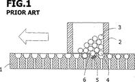
ボールグリッドアレイ技術は、今日、高密度IC部品を回路基板上に連結する上で一般的である。1997年8月12日に松下電器産業株式会社に付与された米国特許第5,655,704号明細書は、スイーピングビンがテンプレート又はステンシル上を通過したときにはんだボールをテンプレート又はステンシルに充填する方法を開示している。しかしながら、かかる方法は、設計それ自体並びにプロセスのばらつき、汚染又は粒子状異物に起因してはんだボールの損傷を非常に受けやすい。損傷の結果として、次にプロセスは実施できず、或いははんだボールをBGAパッケージ上に付着させる目的は、達成できない。
したがって、本発明の目的は、ボールグリッドアレイテンプレートをはんだボールで満たす装置及び方法を提供することにある。
本発明の更に別の目的は、位置決め穴を有するボールグリッドアレイテンプレートに複数の小形はんだボールう充填する装置であって、
軸線が制御装置に回転自在に取り付けられたベースプレートを有し、ボールグリッドアレイテンプレートは、ベースプレートと同時に回転するようベースプレートに取り付けられ、
ベースプレートの頂面上に摺動自在に設けられていて、ベースプレートと一緒に回転するボール供給ビンを有し、ボール供給ビンの摺動運動は、駆動手段、例えばモータによって制御され、ボールグリッドアレイテンプレートは、ベースプレートの軸線回りに回転し、ボール供給ビンは、実質的に矩形であって、3つの垂直側部で包囲され、ボールグリッドアレイテンプレートの近くに位置する第4の垂直側部は、ボールゲートであり、ボールゲートは、その軸線回りに回動し、常態では、ボールゲートの下面のところに位置決めされた停止ピン等、例えば停止縁部によって休止状態になっており、
ベースプレートからのボールゲートの高さとほぼ同じ高さ位置でベースプレートの両端部のところに位置決めされていて、ボールゲートの開放/閉鎖位置をモニタする検出装置を有し、
ボール供給ビンによって包囲された複数の小形はんだボールを有し、ベースプレートをボールグリッドアレイテンプレートに向かって傾斜させると、ボール供給ビンは、ボールグリッドアレイテンプレートに向かって摺動してこの上に位置し、そのようにした場合、テンプレート上の位置決め穴をはんだボールで満たし、次に、ベースプレートを逆方向に傾斜させると、ボール供給ビンは摺動して他端部に戻り、それと同時に、過剰のはんだボールが供給ビン内へ落下して戻ることを特徴とする装置を提供することにある。
本明細書には発明の特徴を記載した特許請求の範囲が別紙として添付されているが、本発明は、図面と関連して以下の説明を読むと一層よく理解されると考えられる。
図7〜図15は、本発明の装置の動作原理を示している。
Claims (13)
- はんだボール充填装置であって、
一端部にボールグリッドアレイテンプレートを備えたベースプレートを有し、はんだボールを受け入れる複数の位置決め穴がボールグリッドアレイテンプレートを貫通して設けられ、ベースプレートは、はんだボールをボールグリッドアレイテンプレートに向かって移動させる第1の回動方向とはんだボールをボールグリッドアレイテンプレートから遠ざける第1の回動方向とは逆の第2の回動方向との間でピボット回りの回動運動を行い、
ベースプレート上に設けられていて、はんだボールを収納保持し、ボールグリッドアレイテンプレート上に配置されるとはんだボールを位置決め穴のうち1以上内に配置するはんだボール供給ビンを有し、
はんだボール供給ビンは、一端部で後部側壁に、且つ反対側の端部で回動式ボールゲートにそれぞれ連結された2つの互いに反対側に位置する側壁を有し、第2の方向におけるベースプレートの回動中、ボールゲートは、ボールグリッドアレイテンプレートから遠ざからなかったはんだボールと接触時にベースプレートに対して回動し、
はんだボール供給ビンをベースプレートに沿ってボールグリッドアレイテンプレートに近づけたり遠ざけたりすることができるモータを有することを特徴とするはんだボール充填装置。 - 後部側壁は、ビンが摺動自在にベースプレート上で動くと、後部側壁がボールグリッドアレイテンプレート上を摺動しないような回動式ボールゲートに対する距離のところに配置されていることを特徴とする請求項1記載のはんだボール充填装置。
- ベースプレートから見て回動式ボールゲートの高さとほぼ同じ高さのところでベースプレートの端部の両方のところに位置決めされた検出装置を更に有していることを特徴とする請求項1記載の装置。
- 検出装置は、全通ビームセンサ又は合焦ビーム反射センサであることを特徴とする請求項3記載の装置。
- ベースプレートは、第1の回動方向に5〜40°の角度回動することを特徴とする請求項1記載の装置。
- ベースプレートは、第2の回動方向に20〜75°の角度回動することを特徴とする請求項1記載の装置。
- ボールグリッドアレイテンプレートの位置決め穴は、真空と連通していることを特徴とする請求項1記載の装置。
- ボールグリッドアレイテンプレートにはんだボールを充填する方法であって、ボールグリッドアレイテンプレートはベースプレートの一端部上に設けられ、複数の位置決め穴がボールグリッドアレイテンプレートを貫通して設けられ、ベースプレートは、第1の回動方向とこれとは逆の第2の回動方向との間で回動運動を行うことができ、はんだボール供給ビンがベースプレート上に設けられ、はんだボール供給ビンは、第1及び第2の回動方向にベースプレート上で摺動でき、前記方法は、
(a)はんだボールをはんだボール供給ビン内に用意する工程と、
(b)ベースプレートを第1の回動方向に回動させてビン内に入っているはんだボールが第1の回動方向に動くことができるようにする工程と、
(c)はんだボール供給ビンを第1の回動方向においてベースプレート上をボールグリッドアレイテンプレートまで動かしてはんだボールが位置決め穴のうち1以上を満たすことができるようにする工程と、
(d)ベースプレートを第2の回動方向に回動させてビン内に入っているはんだボールが第2の回動方向にボールグリッドアレイテンプレートから遠ざかることができるようにする工程と、
(e)はんだボール供給ビンを第2の回動方向でベースプレート上で動かす工程とを有し、
ビンは、はんだボールを、一端部で後部側壁に、且つ反対側の端部で回動式ボールゲートにそれぞれ連結された2つの互いに反対側に位置した側壁の間に保持でき、工程(e)の実施中、ボールゲートは、ボールグリッドアレイテンプレートから遠ざからなかったはんだボールとの接触時にベースプレートに対して回動することを特徴とする方法。 - ベースプレートを第1の回動方向に5〜40°の角度回動させることを特徴とする請求項8記載の方法。
- ベースプレートを第2の回動方向に20〜75°の角度回動させることを特徴とする請求項8記載の方法。
- 工程(e)の実施後、ベースプレートを水平位置まで回動させる工程を更に有していることを特徴とする請求項8記載の方法。
- 第1の回動方向は、時計回りの方向であることを特徴とする請求項8記載の方法。
- 第2の回動方向は、反時計回りの方向であることを特徴とする請求項8記載の方法。
Applications Claiming Priority (2)
| Application Number | Priority Date | Filing Date | Title |
|---|---|---|---|
| SG200206254 | 2002-10-14 | ||
| PCT/SG2003/000246 WO2004035253A1 (en) | 2002-10-14 | 2003-10-13 | An apparatus and method for filling a ball grid array template |
Publications (3)
| Publication Number | Publication Date |
|---|---|
| JP2006503437A JP2006503437A (ja) | 2006-01-26 |
| JP2006503437A5 JP2006503437A5 (ja) | 2007-02-15 |
| JP4528626B2 true JP4528626B2 (ja) | 2010-08-18 |
Family
ID=32105814
Family Applications (1)
| Application Number | Title | Priority Date | Filing Date |
|---|---|---|---|
| JP2004545151A Expired - Lifetime JP4528626B2 (ja) | 2002-10-14 | 2003-10-13 | ボールグリッドアレイテンプレートを充填する装置及び方法 |
Country Status (6)
| Country | Link |
|---|---|
| US (1) | US7458499B2 (ja) |
| JP (1) | JP4528626B2 (ja) |
| CN (1) | CN1703295A (ja) |
| AU (1) | AU2003273208A1 (ja) |
| TW (1) | TWI272708B (ja) |
| WO (1) | WO2004035253A1 (ja) |
Families Citing this family (23)
| Publication number | Priority date | Publication date | Assignee | Title |
|---|---|---|---|---|
| JP4576424B2 (ja) * | 2005-03-30 | 2010-11-10 | 富士通株式会社 | ボール捕捉装置、半田ボール配置装置、ボール捕捉方法、および半田ボール配置方法 |
| TWI458410B (zh) * | 2006-11-22 | 2014-10-21 | Rokko Ventures Pte Ltd | 植球裝置與方法之改良 |
| CN101276759B (zh) * | 2007-03-26 | 2012-10-10 | 矽品精密工业股份有限公司 | 焊球植球设备及其撷取装置 |
| US20080308612A1 (en) * | 2007-06-15 | 2008-12-18 | Best Inc. | Manual method for reballing using a solder preform |
| US7802901B2 (en) * | 2007-09-25 | 2010-09-28 | Cree, Inc. | LED multi-chip lighting units and related methods |
| JP5056491B2 (ja) * | 2007-11-02 | 2012-10-24 | イビデン株式会社 | 半田ボール搭載装置 |
| WO2009102281A1 (en) * | 2008-02-14 | 2009-08-20 | Aurigin Technology Pte Ltd | Apparatus and method for solder ball filing |
| US7780063B2 (en) * | 2008-05-15 | 2010-08-24 | International Business Machines Corporation | Techniques for arranging solder balls and forming bumps |
| SG157985A1 (en) * | 2008-06-24 | 2010-01-29 | Rokko Ventures Pte Ltd | Method and apparatus for solder ball placement |
| CN102122606B (zh) * | 2010-11-16 | 2012-07-18 | 上海微松工业自动化有限公司 | 一种晶圆级封装微球自动收集及供球循环设备 |
| US8813350B2 (en) * | 2011-06-03 | 2014-08-26 | Seagate Technology Llc | Solder ball pattern forming |
| CN102956513A (zh) * | 2011-08-18 | 2013-03-06 | 深南电路有限公司 | 一种球栅阵列器件的植球方法、系统及其夹具 |
| TWI476884B (zh) * | 2012-11-21 | 2015-03-11 | All Ring Tech Co Ltd | A Method and Device for Filling Ball Grid Array Fixture |
| TWI469295B (zh) * | 2012-11-21 | 2015-01-11 | All Ring Tech Co Ltd | A Method and Device for Filling Ball Grid Array Fixture |
| US8955735B2 (en) * | 2013-05-17 | 2015-02-17 | Zen Voce Corporation | Method for enhancing the yield rate of ball implanting of a substrate of an integrated circuit |
| CN103418875A (zh) * | 2013-08-20 | 2013-12-04 | 歌尔声学股份有限公司 | 自动植入锡球装置 |
| US9120170B2 (en) * | 2013-11-01 | 2015-09-01 | Zen Voce Corporation | Apparatus and method for placing and mounting solder balls on an integrated circuit substrate |
| CN104485300B (zh) * | 2014-12-10 | 2017-11-24 | 华进半导体封装先导技术研发中心有限公司 | 磁性非对称型柱或核球的植球治具及植球方法 |
| CN105855659B (zh) * | 2016-06-27 | 2017-12-19 | 上海嘉强自动化技术有限公司 | 一种微型锡球焊接的送料装置 |
| SG10201701738VA (en) * | 2017-03-03 | 2018-10-30 | Aurigin Tech Pte Ltd | Apparatus And Method For Filling A Ball Grid Array |
| CN109300815A (zh) * | 2018-10-12 | 2019-02-01 | 济南晶恒电子有限责任公司 | 圆柱形无脚器件引线自动装填机 |
| CN109436848B (zh) * | 2018-10-30 | 2020-09-29 | 立讯精密工业(滁州)有限公司 | 一种锡球送料机构 |
| US11247285B1 (en) * | 2020-04-03 | 2022-02-15 | Seagate Technology Llc | Fluidization of agglomerated solder microspheres |
Family Cites Families (9)
| Publication number | Priority date | Publication date | Assignee | Title |
|---|---|---|---|---|
| US5551216A (en) * | 1994-09-14 | 1996-09-03 | Vanguard Automation, Inc. | Method and apparatus for filling a ball grid array |
| JP2792596B2 (ja) * | 1994-11-07 | 1998-09-03 | キヤノン電子株式会社 | はんだチップの実装方法及び実装装置及び供給装置及び整列装置及び吸着ヘッド及び回路基板 |
| US5762258A (en) * | 1996-07-23 | 1998-06-09 | International Business Machines Corporation | Method of making an electronic package having spacer elements |
| US6604673B1 (en) | 1999-03-17 | 2003-08-12 | Novatec Sa | Filling device and method for filling balls in the apertures of a ball-receiving element |
| US6276598B1 (en) | 1999-07-13 | 2001-08-21 | Asm Assembly Automation Ltd. | Method and apparatus for ball placement |
| JP3552610B2 (ja) | 1999-10-22 | 2004-08-11 | 松下電器産業株式会社 | 導電性ボールの移載装置および移載方法並びに導電性ボールの供給装置および供給方法 |
| JP3619410B2 (ja) * | 1999-11-18 | 2005-02-09 | 株式会社ルネサステクノロジ | バンプ形成方法およびそのシステム |
| JP4233190B2 (ja) | 1999-11-30 | 2009-03-04 | 日立ビアメカニクス株式会社 | はんだボールの搭載方法およびその装置 |
| US6766938B2 (en) | 2002-01-08 | 2004-07-27 | Asm Assembly Automation Ltd. | Apparatus and method of placing solder balls onto a substrate |
-
2002
- 2002-11-06 TW TW091132644A patent/TWI272708B/zh not_active IP Right Cessation
-
2003
- 2003-10-13 AU AU2003273208A patent/AU2003273208A1/en not_active Abandoned
- 2003-10-13 WO PCT/SG2003/000246 patent/WO2004035253A1/en active Application Filing
- 2003-10-13 JP JP2004545151A patent/JP4528626B2/ja not_active Expired - Lifetime
- 2003-10-13 CN CNA2003801012631A patent/CN1703295A/zh active Pending
- 2003-10-13 US US10/531,611 patent/US7458499B2/en active Active
Also Published As
| Publication number | Publication date |
|---|---|
| CN1703295A (zh) | 2005-11-30 |
| WO2004035253A1 (en) | 2004-04-29 |
| US7458499B2 (en) | 2008-12-02 |
| US20060169743A1 (en) | 2006-08-03 |
| TWI272708B (en) | 2007-02-01 |
| JP2006503437A (ja) | 2006-01-26 |
| AU2003273208A1 (en) | 2004-05-04 |
| TW200406051A (en) | 2004-04-16 |
Similar Documents
| Publication | Publication Date | Title |
|---|---|---|
| JP4528626B2 (ja) | ボールグリッドアレイテンプレートを充填する装置及び方法 | |
| US5499487A (en) | Method and apparatus for filling a ball grid array | |
| US6766938B2 (en) | Apparatus and method of placing solder balls onto a substrate | |
| JP2001148395A (ja) | バンプ形成方法およびそのシステム | |
| US6119927A (en) | Method and apparatus for placing and attaching solder balls to substrates | |
| TW400628B (en) | Solder ball placement apparatus | |
| JP2006503437A5 (ja) | ||
| JP3962197B2 (ja) | バンプ形成システム | |
| JP4068304B2 (ja) | 半田材料製形状部品の配置、再溶融方法およびその装置 | |
| WO2009102281A1 (en) | Apparatus and method for solder ball filing | |
| MXPA97001966A (en) | Method and apparatus for filling a grid device for bo | |
| WO1996009744A2 (en) | Method and apparatus for filling a ball grid array | |
| JP4232861B2 (ja) | はんだボールの搭載方法 | |
| KR102507065B1 (ko) | 반도체칩 본딩장치 | |
| KR200286754Y1 (ko) | 반도체 패키지 제조 장비 | |
| JP3228264B2 (ja) | はんだボール搭載装置及び搭載方法 | |
| JPH09306919A (ja) | 半田ボール等の供給装置 | |
| JP2000077837A (ja) | 半田ボール搭載装置及び搭載方法 | |
| CN110023020B (zh) | 用于填充球栅阵列的设备和方法 | |
| JP2018170513A (ja) | ばら部品供給装置、部品実装装置およびばら部品供給方法 | |
| JP3395614B2 (ja) | 導電性ボールの移載装置および移載方法 | |
| JP3211802B2 (ja) | エキストラボールの検出方法 | |
| WO1998047330A1 (en) | Solder ball loading mechanism | |
| JP3301425B2 (ja) | 導電性ボールの搭載装置および搭載方法 | |
| JP3211803B2 (ja) | エキストラボールの検出方法 |
Legal Events
| Date | Code | Title | Description |
|---|---|---|---|
| A521 | Request for written amendment filed |
Free format text: JAPANESE INTERMEDIATE CODE: A523 Effective date: 20061013 |
|
| A621 | Written request for application examination |
Free format text: JAPANESE INTERMEDIATE CODE: A621 Effective date: 20061013 |
|
| A521 | Request for written amendment filed |
Free format text: JAPANESE INTERMEDIATE CODE: A523 Effective date: 20061221 |
|
| A977 | Report on retrieval |
Free format text: JAPANESE INTERMEDIATE CODE: A971007 Effective date: 20090331 |
|
| A131 | Notification of reasons for refusal |
Free format text: JAPANESE INTERMEDIATE CODE: A131 Effective date: 20091005 |
|
| A601 | Written request for extension of time |
Free format text: JAPANESE INTERMEDIATE CODE: A601 Effective date: 20091228 |
|
| A602 | Written permission of extension of time |
Free format text: JAPANESE INTERMEDIATE CODE: A602 Effective date: 20100108 |
|
| A521 | Request for written amendment filed |
Free format text: JAPANESE INTERMEDIATE CODE: A523 Effective date: 20100402 |
|
| TRDD | Decision of grant or rejection written | ||
| A01 | Written decision to grant a patent or to grant a registration (utility model) |
Free format text: JAPANESE INTERMEDIATE CODE: A01 Effective date: 20100524 |
|
| A01 | Written decision to grant a patent or to grant a registration (utility model) |
Free format text: JAPANESE INTERMEDIATE CODE: A01 |
|
| A61 | First payment of annual fees (during grant procedure) |
Free format text: JAPANESE INTERMEDIATE CODE: A61 Effective date: 20100607 |
|
| FPAY | Renewal fee payment (event date is renewal date of database) |
Free format text: PAYMENT UNTIL: 20130611 Year of fee payment: 3 |
|
| R150 | Certificate of patent or registration of utility model |
Free format text: JAPANESE INTERMEDIATE CODE: R150 Ref document number: 4528626 Country of ref document: JP Free format text: JAPANESE INTERMEDIATE CODE: R150 |
|
| FPAY | Renewal fee payment (event date is renewal date of database) |
Free format text: PAYMENT UNTIL: 20130611 Year of fee payment: 3 |
|
| FPAY | Renewal fee payment (event date is renewal date of database) |
Free format text: PAYMENT UNTIL: 20140611 Year of fee payment: 4 |
|
| R250 | Receipt of annual fees |
Free format text: JAPANESE INTERMEDIATE CODE: R250 |
|
| R250 | Receipt of annual fees |
Free format text: JAPANESE INTERMEDIATE CODE: R250 |
|
| R250 | Receipt of annual fees |
Free format text: JAPANESE INTERMEDIATE CODE: R250 |
|
| R250 | Receipt of annual fees |
Free format text: JAPANESE INTERMEDIATE CODE: R250 |
|
| R250 | Receipt of annual fees |
Free format text: JAPANESE INTERMEDIATE CODE: R250 |
|
| R250 | Receipt of annual fees |
Free format text: JAPANESE INTERMEDIATE CODE: R250 |
|
| R250 | Receipt of annual fees |
Free format text: JAPANESE INTERMEDIATE CODE: R250 |
|
| R250 | Receipt of annual fees |
Free format text: JAPANESE INTERMEDIATE CODE: R250 |
|
| R250 | Receipt of annual fees |
Free format text: JAPANESE INTERMEDIATE CODE: R250 |
|
| R250 | Receipt of annual fees |
Free format text: JAPANESE INTERMEDIATE CODE: R250 |
|
| R250 | Receipt of annual fees |
Free format text: JAPANESE INTERMEDIATE CODE: R250 |
|
| EXPY | Cancellation because of completion of term |