JP4528626B2 - Apparatus and method for filling a ball grid array template - Google Patents
Apparatus and method for filling a ball grid array template Download PDFInfo
- Publication number
- JP4528626B2 JP4528626B2 JP2004545151A JP2004545151A JP4528626B2 JP 4528626 B2 JP4528626 B2 JP 4528626B2 JP 2004545151 A JP2004545151 A JP 2004545151A JP 2004545151 A JP2004545151 A JP 2004545151A JP 4528626 B2 JP4528626 B2 JP 4528626B2
- Authority
- JP
- Japan
- Prior art keywords
- ball
- base plate
- grid array
- solder
- ball grid
- Prior art date
- Legal status (The legal status is an assumption and is not a legal conclusion. Google has not performed a legal analysis and makes no representation as to the accuracy of the status listed.)
- Expired - Lifetime
Links
- 238000000034 method Methods 0.000 title claims description 25
- 229910000679 solder Inorganic materials 0.000 claims description 107
- 238000001514 detection method Methods 0.000 claims description 3
- 238000004891 communication Methods 0.000 claims description 2
- 230000004907 flux Effects 0.000 description 5
- 239000000758 substrate Substances 0.000 description 5
- 238000011109 contamination Methods 0.000 description 3
- 238000010586 diagram Methods 0.000 description 2
- 230000000284 resting effect Effects 0.000 description 2
- 230000003068 static effect Effects 0.000 description 2
- 238000012546 transfer Methods 0.000 description 2
- 230000002159 abnormal effect Effects 0.000 description 1
- 238000007796 conventional method Methods 0.000 description 1
- 238000000151 deposition Methods 0.000 description 1
- 238000013461 design Methods 0.000 description 1
- 238000005516 engineering process Methods 0.000 description 1
- 230000005484 gravity Effects 0.000 description 1
- 239000007788 liquid Substances 0.000 description 1
- 238000012544 monitoring process Methods 0.000 description 1
- 238000010408 sweeping Methods 0.000 description 1
Images


Classifications
-
- B—PERFORMING OPERATIONS; TRANSPORTING
- B23—MACHINE TOOLS; METAL-WORKING NOT OTHERWISE PROVIDED FOR
- B23K—SOLDERING OR UNSOLDERING; WELDING; CLADDING OR PLATING BY SOLDERING OR WELDING; CUTTING BY APPLYING HEAT LOCALLY, e.g. FLAME CUTTING; WORKING BY LASER BEAM
- B23K1/00—Soldering, e.g. brazing, or unsoldering
- B23K1/0008—Soldering, e.g. brazing, or unsoldering specially adapted for particular articles or work
- B23K1/0016—Brazing of electronic components
-
- B—PERFORMING OPERATIONS; TRANSPORTING
- B23—MACHINE TOOLS; METAL-WORKING NOT OTHERWISE PROVIDED FOR
- B23K—SOLDERING OR UNSOLDERING; WELDING; CLADDING OR PLATING BY SOLDERING OR WELDING; CUTTING BY APPLYING HEAT LOCALLY, e.g. FLAME CUTTING; WORKING BY LASER BEAM
- B23K3/00—Tools, devices, or special appurtenances for soldering, e.g. brazing, or unsoldering, not specially adapted for particular methods
- B23K3/06—Solder feeding devices; Solder melting pans
- B23K3/0607—Solder feeding devices
- B23K3/0623—Solder feeding devices for shaped solder piece feeding, e.g. preforms, bumps, balls, pellets, droplets
-
- H—ELECTRICITY
- H01—ELECTRIC ELEMENTS
- H01L—SEMICONDUCTOR DEVICES NOT COVERED BY CLASS H10
- H01L21/00—Processes or apparatus adapted for the manufacture or treatment of semiconductor or solid state devices or of parts thereof
- H01L21/02—Manufacture or treatment of semiconductor devices or of parts thereof
- H01L21/04—Manufacture or treatment of semiconductor devices or of parts thereof the devices having at least one potential-jump barrier or surface barrier, e.g. PN junction, depletion layer or carrier concentration layer
- H01L21/48—Manufacture or treatment of parts, e.g. containers, prior to assembly of the devices, using processes not provided for in a single one of the subgroups H01L21/06 - H01L21/326
- H01L21/4814—Conductive parts
- H01L21/4846—Leads on or in insulating or insulated substrates, e.g. metallisation
- H01L21/4853—Connection or disconnection of other leads to or from a metallisation, e.g. pins, wires, bumps
-
- H—ELECTRICITY
- H01—ELECTRIC ELEMENTS
- H01L—SEMICONDUCTOR DEVICES NOT COVERED BY CLASS H10
- H01L24/00—Arrangements for connecting or disconnecting semiconductor or solid-state bodies; Methods or apparatus related thereto
- H01L24/01—Means for bonding being attached to, or being formed on, the surface to be connected, e.g. chip-to-package, die-attach, "first-level" interconnects; Manufacturing methods related thereto
- H01L24/10—Bump connectors ; Manufacturing methods related thereto
- H01L24/11—Manufacturing methods
-
- B—PERFORMING OPERATIONS; TRANSPORTING
- B23—MACHINE TOOLS; METAL-WORKING NOT OTHERWISE PROVIDED FOR
- B23K—SOLDERING OR UNSOLDERING; WELDING; CLADDING OR PLATING BY SOLDERING OR WELDING; CUTTING BY APPLYING HEAT LOCALLY, e.g. FLAME CUTTING; WORKING BY LASER BEAM
- B23K2101/00—Articles made by soldering, welding or cutting
- B23K2101/36—Electric or electronic devices
- B23K2101/40—Semiconductor devices
-
- H—ELECTRICITY
- H01—ELECTRIC ELEMENTS
- H01L—SEMICONDUCTOR DEVICES NOT COVERED BY CLASS H10
- H01L2224/00—Indexing scheme for arrangements for connecting or disconnecting semiconductor or solid-state bodies and methods related thereto as covered by H01L24/00
- H01L2224/01—Means for bonding being attached to, or being formed on, the surface to be connected, e.g. chip-to-package, die-attach, "first-level" interconnects; Manufacturing methods related thereto
- H01L2224/10—Bump connectors; Manufacturing methods related thereto
- H01L2224/12—Structure, shape, material or disposition of the bump connectors prior to the connecting process
- H01L2224/13—Structure, shape, material or disposition of the bump connectors prior to the connecting process of an individual bump connector
- H01L2224/13001—Core members of the bump connector
- H01L2224/13099—Material
-
- H—ELECTRICITY
- H01—ELECTRIC ELEMENTS
- H01L—SEMICONDUCTOR DEVICES NOT COVERED BY CLASS H10
- H01L2924/00—Indexing scheme for arrangements or methods for connecting or disconnecting semiconductor or solid-state bodies as covered by H01L24/00
- H01L2924/01—Chemical elements
- H01L2924/01005—Boron [B]
-
- H—ELECTRICITY
- H01—ELECTRIC ELEMENTS
- H01L—SEMICONDUCTOR DEVICES NOT COVERED BY CLASS H10
- H01L2924/00—Indexing scheme for arrangements or methods for connecting or disconnecting semiconductor or solid-state bodies as covered by H01L24/00
- H01L2924/01—Chemical elements
- H01L2924/01006—Carbon [C]
-
- H—ELECTRICITY
- H01—ELECTRIC ELEMENTS
- H01L—SEMICONDUCTOR DEVICES NOT COVERED BY CLASS H10
- H01L2924/00—Indexing scheme for arrangements or methods for connecting or disconnecting semiconductor or solid-state bodies as covered by H01L24/00
- H01L2924/01—Chemical elements
- H01L2924/01027—Cobalt [Co]
-
- H—ELECTRICITY
- H01—ELECTRIC ELEMENTS
- H01L—SEMICONDUCTOR DEVICES NOT COVERED BY CLASS H10
- H01L2924/00—Indexing scheme for arrangements or methods for connecting or disconnecting semiconductor or solid-state bodies as covered by H01L24/00
- H01L2924/01—Chemical elements
- H01L2924/01033—Arsenic [As]
-
- H—ELECTRICITY
- H01—ELECTRIC ELEMENTS
- H01L—SEMICONDUCTOR DEVICES NOT COVERED BY CLASS H10
- H01L2924/00—Indexing scheme for arrangements or methods for connecting or disconnecting semiconductor or solid-state bodies as covered by H01L24/00
- H01L2924/01—Chemical elements
- H01L2924/01079—Gold [Au]
-
- H—ELECTRICITY
- H01—ELECTRIC ELEMENTS
- H01L—SEMICONDUCTOR DEVICES NOT COVERED BY CLASS H10
- H01L2924/00—Indexing scheme for arrangements or methods for connecting or disconnecting semiconductor or solid-state bodies as covered by H01L24/00
- H01L2924/01—Chemical elements
- H01L2924/01082—Lead [Pb]
-
- H—ELECTRICITY
- H01—ELECTRIC ELEMENTS
- H01L—SEMICONDUCTOR DEVICES NOT COVERED BY CLASS H10
- H01L2924/00—Indexing scheme for arrangements or methods for connecting or disconnecting semiconductor or solid-state bodies as covered by H01L24/00
- H01L2924/013—Alloys
- H01L2924/014—Solder alloys
-
- H—ELECTRICITY
- H05—ELECTRIC TECHNIQUES NOT OTHERWISE PROVIDED FOR
- H05K—PRINTED CIRCUITS; CASINGS OR CONSTRUCTIONAL DETAILS OF ELECTRIC APPARATUS; MANUFACTURE OF ASSEMBLAGES OF ELECTRICAL COMPONENTS
- H05K3/00—Apparatus or processes for manufacturing printed circuits
- H05K3/30—Assembling printed circuits with electric components, e.g. with resistor
- H05K3/32—Assembling printed circuits with electric components, e.g. with resistor electrically connecting electric components or wires to printed circuits
- H05K3/34—Assembling printed circuits with electric components, e.g. with resistor electrically connecting electric components or wires to printed circuits by soldering
- H05K3/3457—Solder materials or compositions; Methods of application thereof
- H05K3/3478—Applying solder preforms; Transferring prefabricated solder patterns
Description
発明の背景
発明の分野
本発明は一般に、ボールグリッドアレイ(BGA)に関し、特に、ボールグリッドアレイテンプレートにはんだボールを充填する装置及び方法に関する。
先行技術の説明
ボールグリッドアレイ技術は、今日、高密度IC部品を回路基板上に連結する上で一般的である。1997年8月12日に松下電器産業株式会社に付与された米国特許第5,655,704号明細書は、スイーピングビンがテンプレート又はステンシル上を通過したときにはんだボールをテンプレート又はステンシルに充填する方法を開示している。しかしながら、かかる方法は、設計それ自体並びにプロセスのばらつき、汚染又は粒子状異物に起因してはんだボールの損傷を非常に受けやすい。損傷の結果として、次にプロセスは実施できず、或いははんだボールをBGAパッケージ上に付着させる目的は、達成できない。
The present invention relates generally to a ball grid array (BGA), and more particularly to an apparatus and method for filling a ball grid array template with solder balls.
DESCRIPTION OF THE PRIOR ART Ball grid array technology is common today for connecting high density IC components on a circuit board. US Pat. No. 5,655,704 granted to Matsushita Electric Industrial Co., Ltd. on August 12, 1997, fills a template or stencil with solder balls when the sweeping bin passes over the template or stencil. A method is disclosed. However, such methods are very susceptible to solder ball damage due to design variations as well as process variations, contamination, or particulate contamination. As a result of the damage, the next process cannot be performed or the purpose of depositing the solder balls on the BGA package cannot be achieved.
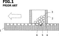
図1は、BGAテンプレートをはんだボールで満たす従来方法を示している。BGAテンプレート1は、複数のはんだボール3を受け入れる複数の穴を備えている。ボールビン2は、テンプレート1上を全体にわたって払ってはんだボール3をテンプレート1の穴の中に配置する。はんだボール3のこの配置ははんだボール3と穴が互いに整列したときにはいつでも起こるので、かかる配置は、はんだボール4がまさに落ち込もうとする特定の穴にボールビン2がまさに到達しようとしたときに起こる場合がある。図1に示すように、この結果として、ボール4がビン2によってだめになる場合がある。別の考えられる状況は、はんだボール6が異物5によって穴の中に嵌り込まない場合である。ビン2は、はんだボール6の頂部を剪断することになる。
FIG. 1 shows a conventional method of filling a BGA template with solder balls. The
図2は、米国特許第5,655,704号明細書に開示されたはんだボール取付け装置を示す斜視図である。図2に示すように、はんだボールは、ステンシル7を通って基板10上に配置される。基板上のフラックスドット11が、はんだボール9を定位置に保持する。しかしながら、これらフラックスドット11が液状ペーストなので、ドット11の体積又は高さは、フラックスドット12の場合量が過剰であれば様々である場合がある。これにより、はんだボール13は、ステンシル7から突き出てはんだボールビン8がボール13上を通っている時に頂部が剪断される。潜在的に、フラックスドットが存在しない場合があり、はんだボールは、通常の高さよりも低く落下し、はんだボール14がビン8によって剪断されることになる。
FIG. 2 is a perspective view showing a solder ball mounting apparatus disclosed in US Pat. No. 5,655,704. As shown in FIG. 2, the solder balls are disposed on the
1996年3月19日にバンガード・オートメーション・インコーポレイテッドに付与された米国特許第5,499,487号明細書は、はんだボールをボールグリッドアレイの状態で配置する装置を開示している。この装置は、内側フェース及び外側フェースを備えていて、水平軸線回りに回転自在なホイールと、ボールグリッドアレイをホイールの内側フェースに取り付ける手段と、ツーリングジグをボールグリッドアレイの位置に対応する位置でホイールの外側フェースに取り付ける手段と、ホイールの底部にはんだボールのリザーバを形成する手段と、ホイールを制御自在に回転させてツーリングジグをジグに設けられた凹部をはんだボールで満たしたり凹部を占めなかった過剰のはんだボールをアレイの表面から除くような仕方でリザーバを通って動かす手段とを有し、内側フェースと外側フェースは、ツーリングジグがリザーバ内のはんだボールに係合することができ、他方ボールグリッドアレイがはんだボールに係合しないような距離互いに分離されている。 U.S. Pat. No. 5,499,487 issued to Vanguard Automation, Inc. on March 19, 1996 discloses an apparatus for placing solder balls in a ball grid array. The device comprises an inner face and an outer face, a wheel rotatable around a horizontal axis, means for attaching the ball grid array to the inner face of the wheel, and a tooling jig at a position corresponding to the position of the ball grid array. A means to attach to the outer face of the wheel, a means to form a solder ball reservoir at the bottom of the wheel, and a wheel that can be controlled to rotate so that the tooling jig does not fill or occupy the recess provided in the jig. Means to move the excess solder balls through the reservoir in such a way as to remove them from the surface of the array, the inner face and the outer face allowing the tooling jig to engage the solder balls in the reservoir, The distance between the ball grid array so that it does not engage the solder balls It is separated.
米国特許第5,551,216号明細書は、ボールグリッドアレイを充填する方法及び装置に関する。この装置は、はんだボールのリザーバと、はんだボールを受け入れるアレイ上に配置された穴を備えるツーリングプレートとを有する。米国特許第6,276,598号明細書は、ボール配置のための方法及び装置に関する。この方法及び装置は、はんだボールをボールグリッドアレイパッケージに移送するのに特に適している。 U.S. Pat. No. 5,551,216 relates to a method and apparatus for filling a ball grid array. The apparatus includes a solder ball reservoir and a tooling plate with holes disposed on the array for receiving the solder balls. US Pat. No. 6,276,598 relates to a method and apparatus for ball placement. This method and apparatus is particularly suitable for transferring solder balls to a ball grid array package.
上述の米国特許第5,499,487号明細書、第5,551,216号明細書及び第6,276,598号明細書に開示された方法は、はんだボールを受け入れる穴のところに真空吸引法式を用い又は用いないで傾斜したテンプレート15上にはんだボール17を自由に流す方式を利用している。この方法は、過剰のはんだボール18及びはんだボール19が静的な力、穴のところの真空漏れ又は基板への取付けの際に用いられるフラックスのようにねばねばしている場合のある異物に起因してテンプレートの表面上又は穴の周りに留まるのを阻止することはない。これら特許文献では、ボールピックヘッド16又はボールグリッドアレイ基板20をテンプレート上に前進させる次の作業の結果として、ピックヘッドの各穴のところ又はボールグリッドアレイ上の各電極のところではんだボール又は多数のボールがだめになる場合がある(図3及び図4に示されている)。
The methods disclosed in the aforementioned U.S. Pat. Nos. 5,499,487, 5,551,216 and 6,276,598 provide vacuum suction at the holes that accept the solder balls. A method is used in which the
1999年7月6日にRSVIバンガード・インコーポレイテッドに付与された米国特許第5,918,792号明細書は、ボールグリッドアレイ及びかかるアレイの金属化パッド又はドットのパターン上にはんだボールを配置する方法を開示している。この装置は、アレイのキャリヤのための細長い凹部が形成された細長いホルダと、凹部の上に位置し、案内レールによって支持されたステンシルと、ステンシルに接触する平らな底面を有し、ステンシルに沿って運動可能な剛性材料のブロックと、ブロックをステンシルに沿って動かしてはんだボールに接触しているビンをステンシルに形成された孔上に動かして孔を満たすようにする手段とを有する。 US Pat. No. 5,918,792 issued to RSVI Vanguard, Inc. on July 6, 1999, places solder balls on a ball grid array and a pattern of metallized pads or dots in such an array. A method is disclosed. The apparatus has an elongate holder formed with an elongate recess for the carrier of the array, a stencil positioned over the recess and supported by a guide rail, and a flat bottom surface in contact with the stencil, along the stencil. And a means for moving the block along the stencil to move the bottle in contact with the solder ball over the hole formed in the stencil to fill the hole.
発明の概要
したがって、本発明の目的は、ボールグリッドアレイテンプレートをはんだボールで満たす装置及び方法を提供することにある。
本発明の更に別の目的は、位置決め穴を有するボールグリッドアレイテンプレートに複数の小形はんだボールう充填する装置であって、
軸線が制御装置に回転自在に取り付けられたベースプレートを有し、ボールグリッドアレイテンプレートは、ベースプレートと同時に回転するようベースプレートに取り付けられ、
ベースプレートの頂面上に摺動自在に設けられていて、ベースプレートと一緒に回転するボール供給ビンを有し、ボール供給ビンの摺動運動は、駆動手段、例えばモータによって制御され、ボールグリッドアレイテンプレートは、ベースプレートの軸線回りに回転し、ボール供給ビンは、実質的に矩形であって、3つの垂直側部で包囲され、ボールグリッドアレイテンプレートの近くに位置する第4の垂直側部は、ボールゲートであり、ボールゲートは、その軸線回りに回動し、常態では、ボールゲートの下面のところに位置決めされた停止ピン等、例えば停止縁部によって休止状態になっており、
ベースプレートからのボールゲートの高さとほぼ同じ高さ位置でベースプレートの両端部のところに位置決めされていて、ボールゲートの開放/閉鎖位置をモニタする検出装置を有し、
ボール供給ビンによって包囲された複数の小形はんだボールを有し、ベースプレートをボールグリッドアレイテンプレートに向かって傾斜させると、ボール供給ビンは、ボールグリッドアレイテンプレートに向かって摺動してこの上に位置し、そのようにした場合、テンプレート上の位置決め穴をはんだボールで満たし、次に、ベースプレートを逆方向に傾斜させると、ボール供給ビンは摺動して他端部に戻り、それと同時に、過剰のはんだボールが供給ビン内へ落下して戻ることを特徴とする装置を提供することにある。
SUMMARY OF THE INVENTION Accordingly, it is an object of the present invention to provide an apparatus and method for filling a ball grid array template with solder balls.
Still another object of the present invention is an apparatus for filling a ball grid array template having positioning holes into a plurality of small solder balls,
The axis has a base plate rotatably attached to the controller, and the ball grid array template is attached to the base plate to rotate simultaneously with the base plate;
A ball supply bin which is slidably provided on the top surface of the base plate and rotates together with the base plate, and the sliding movement of the ball supply bin is controlled by a driving means, for example, a motor; Rotates about the axis of the base plate, the ball supply bin is substantially rectangular and is surrounded by three vertical sides, and the fourth vertical side located near the ball grid array template is a ball It is a gate, the ball gate rotates around its axis, and is normally in a resting state by a stop pin, for example, a stop edge positioned at the lower surface of the ball gate,
Positioned at both ends of the base plate at approximately the same height as the height of the ball gate from the base plate and having a detection device for monitoring the open / closed position of the ball gate;
Having a plurality of small solder balls surrounded by a ball supply bin and tilting the base plate toward the ball grid array template, the ball supply bin slides toward the ball grid array template and sits on it. In such a case, when the positioning hole on the template is filled with solder balls and then the base plate is tilted in the opposite direction, the ball supply bin slides back to the other end and at the same time excess solder It is an object of the present invention to provide an apparatus characterized in that a ball falls into a supply bin and returns.
本発明の更に別の目的は、複数の位置決め穴を有するボールグリッドアレイテンプレート上にはんだボールを充填する方法であって、前記ボールグリッドアレイテンプレートを回動ベースプレートの一端部に位置決めする工程と、ベースプレートの一端部のところに摺動自在に位置決めされ、ベースプレート上で摺動可能なボール供給ビン内に複数のはんだボールを導入する工程と、ベースプレートを時計回りに回転させ、ボール供給ビンがボールグリッドアレイテンプレートに向かって摺動してボール供給ビン内に入っているはんだボールがテンプレートの位置決め穴をそれぞれ一つずつ満たすことができ、ボール供給ビンの摺動運動は、駆動手段、例えばモータによって制御されるようにする工程と、ベースプレートを反時計回りに回転させ、ボール供給ビンを摺動させてその初期位置に戻し、そのようにする際、過剰のはんだボールをボールグリッドアレイテンプレート上から除くようにする工程とを有する方法を提供することにある。 Still another object of the present invention is a method of filling solder balls onto a ball grid array template having a plurality of positioning holes, the step of positioning the ball grid array template at one end of a rotating base plate, and a base plate A step of introducing a plurality of solder balls into a ball supply bin slidably positioned at one end of the base plate and slidable on the base plate, and rotating the base plate clockwise so that the ball supply bin is in a ball grid array. The solder balls that slide toward the template and enter the ball supply bin can fill the positioning holes of the template one by one, and the sliding movement of the ball supply bin is controlled by driving means, for example, a motor. And the base plate is rotated counterclockwise Was returned to its initial position by sliding the ball supplying bottle, when to do so is to provide a method and a step of the excess solder balls to exclude from the ball grid array on the template.
本発明の別の目的は、真空によりはんだボールを除去するようボールグリッドアレイテンプレート上に下降し、ボールグリッドアレイ基板に移送するボールピックヘッドを更に有していることを特徴とするボールグリッドアレイテンプレートにはんだボールを充填する装置を提供することにある。 Another object of the present invention is to provide a ball grid array template further comprising a ball pick head that descends onto the ball grid array template and removes the solder balls by vacuum and transfers it to the ball grid array substrate. An object of the present invention is to provide an apparatus for filling solder balls.
本発明の更に別の目的は、ベースプレートを水平上で5〜40°の角度、時計回りの方向に傾けることを特徴とするボールグリッドアレイテンプレートにはんだボールを充填する方法を提供することにある。 It is still another object of the present invention to provide a method of filling a ball grid array template with solder balls, wherein the base plate is tilted in the clockwise direction at an angle of 5 to 40 degrees horizontally.
本発明の更に別の目的は、ベースプレートを水平の下で20〜75°の角度、反時計回りの方向に傾けることを特徴とするボールグリッドアレイテンプレートにはんだボールを充填する方法を提供することにある。 Still another object of the present invention is to provide a method of filling a ball grid array template with solder balls, characterized in that the base plate is tilted in the counterclockwise direction at an angle of 20-75 ° under the horizontal. is there.
次に、本発明の実施形態を添付の図面を参照して一例として説明する。 Embodiments of the present invention will now be described by way of example with reference to the accompanying drawings.
発明の詳細な説明
本明細書には発明の特徴を記載した特許請求の範囲が別紙として添付されているが、本発明は、図面と関連して以下の説明を読むと一層よく理解されると考えられる。
DETAILED DESCRIPTION OF THE INVENTION While the specification is accompanied by the appended claims that set forth the features of the invention, the invention will be better understood when the following description is read in conjunction with the drawings. Conceivable.
今図5を参照すると、本発明に従ってはんだボールをボールグリッドアレイテンプレート上に充填する装置が示されている。この装置は、軸線2が制御装置に回転自在に取り付けられたベースプレート1と、ベースプレート1の一端部の頂面に取り付けられていて、ベースプレート1が時計回り又は反時計回りに回転(傾斜)すると、ベースプレート1と同時に回転するようになるボールグリッドアレイテンプレート3と、ボールグリッドアレイテンプレート3の位置に対応したベースプレート1の他端部の頂面上に摺動自在に設けられていて、モータによって駆動され、ベースプレート1がベースプレート1の軸線2回りに回転している間、ベースプレート1に沿って動くことができる実質的に矩形の形をしたボール供給ビン4とを有する。この好ましい実施形態によれば、ボール供給ビン4は、3つの垂直側部で包囲され、ボールグリッドアレイテンプレート3の近くに位置した第4の垂直側部は、ボールゲート5を備えている。ボールゲート5は、その軸線6回りに回動し、常態では、ベースプレート1が時計回り又は反時計回りに回転すると、ボールゲート5の下面のところに配置された停止ピン7によって休止状態になっている。ボールグリッドアレイテンプレート3は、頂面にはんだボール10を保持する複数の位置決め穴12を備え、1つの位置決め穴12は、図5に示すようにはんだボール10を1つしか受け入れない。 検出装置8、例えば全通ビームセンサ又は合焦ビーム反射センサが、ベースプレート1から見てボールゲート5の高さとほぼ同じ高さのところでベースプレート1の端部の両方のところに位置決めされた状態で支持されていて、ボールゲート5の開放/閉鎖位置をモニタするようになっている。ボールゲート5が開放位置にあれば、これにより作動に異常のあるらしいことが分かる。ボールゲート5は、ボールゲート5の重量が軸線6回りに回動するような仕方で設計されており、この重量により、ボールゲート5ははんだボール11をボール供給ビン4内に収容する閉鎖壁を形成するようになる。
Referring now to FIG. 5, an apparatus for filling solder ball onto a ball grid array template in accordance with the present invention is shown. This device has a
図5に示すように、複数の小形はんだボール(ばらのまま)11が、ボール供給ビン4によって包囲されている。ボールピックヘッド9をボールテンプレート3の上方に位置決めし、これを下降させて真空作用によりボールグリッドアレイテンプレート3上のはんだボール10を除いてこれらをBGA基板19に移送するようになっている(図15参照)。
As shown in FIG. 5, a plurality of small solder balls (as loose pieces) 11 are surrounded by the
本発明によれば、真空18は、ボールグリッドアレイテンプレート3の個々の位置決め穴12と連通した状態でボールグリッドアレイテンプレート3の下に設けられたチャンバ13に提供され、はんだボール10の充填を助けるようになっている(図7及び図8参照)。
図7〜図15は、本発明の装置の動作原理を示している。
In accordance with the present invention, a
7 to 15 show the principle of operation of the device of the present invention.
この装置の最初の作動時、はんだボール10が位置決め穴12には存在しない状態でベースプレート1は、ボールグリッドアレイテンプレート3と共に水平位置にある(図6に示すように)。図6に示すように、はんだボール11は、ボール供給ビン4内に入っており、ボールゲート5は、閉鎖位置にある。
During initial operation of the apparatus, the
図7を参照すると、ベースプレート1は、水平より上方に約5°〜40°まで時計回りに傾斜し又はこれを回転させる。回転角度は、ボール供給ビン4内のはんだボール11がボールゲート5に向かって散らばって次の工程におけるボールグリッドアレイテンプレート3全体上へのボールの配置の可能性を最高に高めることができるかどうかで決まる。ボールゲート5は、はんだボール11を供給ビン4内に保持する閉鎖壁を形成する。
Referring to FIG. 7, the
図8に示すように、ボール供給ビン4がボールグリッドアレイテンプレート3上でテンプレート3に向かって摺動し、このようにする際、供給ビン4内のはんだボール11は、テンプレート3の表面の位置決め穴12内に入れられる。チャンバ13に連結された真空手段18が、はんだボール10をテンプレート3の位置決め穴12内に充填するのを助ける。
As shown in FIG. 8, the
図9を参照すると、次にベースプレート1を水平より下へ約20°〜75°まで反時計回りに傾斜させ又は回転させる。同様に、回転角度は、ボール供給ビン4内のはんだボール11がボールゲート5からビン4の遠方端部に向かって重力の作用で且つボールゲート5を軸線6回りに回動させる回転トルクとバランスを取る量だけ自由に落下できるかどうかで決定される。
Referring to FIG. 9, the
はんだボール11が代表的には非常に小さく、直径が0.2mmという小形であるということにより、符号14で示す幾つかの残りのはんだボールは、静電荷、湿度、汚染又は真空漏れに起因してベースプレート1の表面15、ボールグリッドアレイテンプレート3又は位置決め穴12周りにくっつく場合がある。
Due to the fact that the
図10に示すように、この角度配向状態では、ボール供給ビン4は、後方に摺動し、そのようにする際、過剰の残りのはんだボール14を払い去る。位置決め穴12内に入っているはんだボール10は、定位置に位置したままであり、チャンバ13内の真空18又は位置決め穴12の深さにより保持される。
As shown in FIG. 10, in this angular orientation state, the
Claims (13)
一端部にボールグリッドアレイテンプレートを備えたベースプレートを有し、はんだボールを受け入れる複数の位置決め穴がボールグリッドアレイテンプレートを貫通して設けられ、ベースプレートは、はんだボールをボールグリッドアレイテンプレートに向かって移動させる第1の回動方向とはんだボールをボールグリッドアレイテンプレートから遠ざける第1の回動方向とは逆の第2の回動方向との間でピボット回りの回動運動を行い、
ベースプレート上に設けられていて、はんだボールを収納保持し、ボールグリッドアレイテンプレート上に配置されるとはんだボールを位置決め穴のうち1以上内に配置するはんだボール供給ビンを有し、
はんだボール供給ビンは、一端部で後部側壁に、且つ反対側の端部で回動式ボールゲートにそれぞれ連結された2つの互いに反対側に位置する側壁を有し、第2の方向におけるベースプレートの回動中、ボールゲートは、ボールグリッドアレイテンプレートから遠ざからなかったはんだボールと接触時にベースプレートに対して回動し、
はんだボール供給ビンをベースプレートに沿ってボールグリッドアレイテンプレートに近づけたり遠ざけたりすることができるモータを有することを特徴とするはんだボール充填装置。A solder ball filling device,
A base plate having a ball grid array template at one end and a plurality of positioning holes for receiving solder balls are provided through the ball grid array template, the base plate moving the solder balls toward the ball grid array template Performing a pivoting movement between the first pivoting direction and the second pivoting direction opposite to the first pivoting direction to move the solder ball away from the ball grid array template;
A solder ball supply bin that is provided on the base plate and stores and holds the solder balls, and when placed on the ball grid array template, places the solder balls in one or more of the positioning holes;
The solder ball supply bin has two opposite side walls connected to the rear side wall at one end and to the pivoting ball gate at the opposite end, respectively, and the base plate in the second direction. During rotation, the ball gate rotates relative to the base plate when in contact with the solder balls that have not moved away from the ball grid array template,
A solder ball filling apparatus comprising a motor capable of moving a solder ball supply bin toward and away from a ball grid array template along a base plate.
(a)はんだボールをはんだボール供給ビン内に用意する工程と、
(b)ベースプレートを第1の回動方向に回動させてビン内に入っているはんだボールが第1の回動方向に動くことができるようにする工程と、
(c)はんだボール供給ビンを第1の回動方向においてベースプレート上をボールグリッドアレイテンプレートまで動かしてはんだボールが位置決め穴のうち1以上を満たすことができるようにする工程と、
(d)ベースプレートを第2の回動方向に回動させてビン内に入っているはんだボールが第2の回動方向にボールグリッドアレイテンプレートから遠ざかることができるようにする工程と、
(e)はんだボール供給ビンを第2の回動方向でベースプレート上で動かす工程とを有し、
ビンは、はんだボールを、一端部で後部側壁に、且つ反対側の端部で回動式ボールゲートにそれぞれ連結された2つの互いに反対側に位置した側壁の間に保持でき、工程(e)の実施中、ボールゲートは、ボールグリッドアレイテンプレートから遠ざからなかったはんだボールとの接触時にベースプレートに対して回動することを特徴とする方法。A method of filling a ball grid array template with solder balls, wherein the ball grid array template is provided on one end of a base plate, a plurality of positioning holes are provided through the ball grid array template, And a second rotation direction opposite to the rotation direction, and a solder ball supply bin is provided on the base plate, and the solder ball supply bin includes the first and second solder ball supply bins. Can slide on the base plate in two rotational directions,
(A) preparing a solder ball in a solder ball supply bin;
(B) rotating the base plate in the first rotation direction so that the solder balls contained in the bin can move in the first rotation direction;
(C) moving the solder ball supply bin on the base plate in the first rotational direction to the ball grid array template so that the solder balls can fill one or more of the positioning holes;
(D) rotating the base plate in the second rotation direction so that the solder balls contained in the bin can be moved away from the ball grid array template in the second rotation direction;
(E) it possesses a step of moving on the base plate with the solder ball supply bins second rotational direction,
The bin can hold a solder ball between two opposite side walls connected to the rear side wall at one end and to the pivoting ball gate at the opposite end, step (e) During the operation, the ball gate is rotated with respect to the base plate when in contact with the solder balls that have not been moved away from the ball grid array template .
Applications Claiming Priority (2)
| Application Number | Priority Date | Filing Date | Title |
|---|---|---|---|
| SG200206254 | 2002-10-14 | ||
| PCT/SG2003/000246 WO2004035253A1 (en) | 2002-10-14 | 2003-10-13 | An apparatus and method for filling a ball grid array template |
Publications (3)
| Publication Number | Publication Date |
|---|---|
| JP2006503437A JP2006503437A (en) | 2006-01-26 |
| JP2006503437A5 JP2006503437A5 (en) | 2007-02-15 |
| JP4528626B2 true JP4528626B2 (en) | 2010-08-18 |
Family
ID=32105814
Family Applications (1)
| Application Number | Title | Priority Date | Filing Date |
|---|---|---|---|
| JP2004545151A Expired - Lifetime JP4528626B2 (en) | 2002-10-14 | 2003-10-13 | Apparatus and method for filling a ball grid array template |
Country Status (6)
| Country | Link |
|---|---|
| US (1) | US7458499B2 (en) |
| JP (1) | JP4528626B2 (en) |
| CN (1) | CN1703295A (en) |
| AU (1) | AU2003273208A1 (en) |
| TW (1) | TWI272708B (en) |
| WO (1) | WO2004035253A1 (en) |
Families Citing this family (23)
| Publication number | Priority date | Publication date | Assignee | Title |
|---|---|---|---|---|
| WO2006103766A1 (en) * | 2005-03-30 | 2006-10-05 | Fujitsu Limited | Ball capturing device, solder ball arrangement device, ball capturing method, and solder ball arranging method |
| KR20090096706A (en) * | 2006-11-22 | 2009-09-14 | 록코 벤처스 피티이 리미티드 | An improved ball mounting apparatus and method |
| CN101276759B (en) * | 2007-03-26 | 2012-10-10 | 矽品精密工业股份有限公司 | Equipment for soldering and planting ball as well as acquisition apparatus |
| US20080308612A1 (en) * | 2007-06-15 | 2008-12-18 | Best Inc. | Manual method for reballing using a solder preform |
| US7802901B2 (en) * | 2007-09-25 | 2010-09-28 | Cree, Inc. | LED multi-chip lighting units and related methods |
| JP5056491B2 (en) * | 2007-11-02 | 2012-10-24 | イビデン株式会社 | Solder ball mounting device |
| WO2009102281A1 (en) * | 2008-02-14 | 2009-08-20 | Aurigin Technology Pte Ltd | Apparatus and method for solder ball filing |
| US7780063B2 (en) * | 2008-05-15 | 2010-08-24 | International Business Machines Corporation | Techniques for arranging solder balls and forming bumps |
| SG157985A1 (en) * | 2008-06-24 | 2010-01-29 | Rokko Ventures Pte Ltd | Method and apparatus for solder ball placement |
| CN102122606B (en) * | 2010-11-16 | 2012-07-18 | 上海微松工业自动化有限公司 | Wafer-level package micro-ball automatic collection, supply and circulation equipment |
| US8813350B2 (en) * | 2011-06-03 | 2014-08-26 | Seagate Technology Llc | Solder ball pattern forming |
| CN102956513A (en) * | 2011-08-18 | 2013-03-06 | 深南电路有限公司 | Method, system and fixture for ball attachment in ball grid array devices |
| TWI476884B (en) * | 2012-11-21 | 2015-03-11 | All Ring Tech Co Ltd | A Method and Device for Filling Ball Grid Array Fixture |
| TWI469295B (en) * | 2012-11-21 | 2015-01-11 | All Ring Tech Co Ltd | A Method and Device for Filling Ball Grid Array Fixture |
| US8955735B2 (en) * | 2013-05-17 | 2015-02-17 | Zen Voce Corporation | Method for enhancing the yield rate of ball implanting of a substrate of an integrated circuit |
| CN103418875A (en) * | 2013-08-20 | 2013-12-04 | 歌尔声学股份有限公司 | Automatic solder ball implantation device |
| US9120170B2 (en) * | 2013-11-01 | 2015-09-01 | Zen Voce Corporation | Apparatus and method for placing and mounting solder balls on an integrated circuit substrate |
| CN104485300B (en) * | 2014-12-10 | 2017-11-24 | 华进半导体封装先导技术研发中心有限公司 | The plant ball tool and ball-establishing method of the asymmetric post of magnetic or caryosphere |
| CN105855659B (en) * | 2016-06-27 | 2017-12-19 | 上海嘉强自动化技术有限公司 | A kind of feed device of miniature tin ball bonding |
| SG10201701738VA (en) * | 2017-03-03 | 2018-10-30 | Aurigin Tech Pte Ltd | Apparatus And Method For Filling A Ball Grid Array |
| CN109300815A (en) * | 2018-10-12 | 2019-02-01 | 济南晶恒电子有限责任公司 | Cylinder is without foot device wire automatic filling machine |
| CN109436848B (en) * | 2018-10-30 | 2020-09-29 | 立讯精密工业(滁州)有限公司 | Tin ball feeding mechanism |
| US11247285B1 (en) * | 2020-04-03 | 2022-02-15 | Seagate Technology Llc | Fluidization of agglomerated solder microspheres |
Family Cites Families (9)
| Publication number | Priority date | Publication date | Assignee | Title |
|---|---|---|---|---|
| US5551216A (en) * | 1994-09-14 | 1996-09-03 | Vanguard Automation, Inc. | Method and apparatus for filling a ball grid array |
| JP2792596B2 (en) * | 1994-11-07 | 1998-09-03 | キヤノン電子株式会社 | Solder chip mounting method, mounting device, supply device, alignment device, suction head, and circuit board |
| US5762258A (en) * | 1996-07-23 | 1998-06-09 | International Business Machines Corporation | Method of making an electronic package having spacer elements |
| EP1163080B1 (en) | 1999-03-17 | 2005-05-11 | Novatec S.A. | Filling device and method for filling balls in the apertures of a ball-receiving element |
| US6276598B1 (en) * | 1999-07-13 | 2001-08-21 | Asm Assembly Automation Ltd. | Method and apparatus for ball placement |
| JP3552610B2 (en) * | 1999-10-22 | 2004-08-11 | 松下電器産業株式会社 | Apparatus and method for transferring conductive balls, and apparatus and method for supplying conductive balls |
| JP3619410B2 (en) * | 1999-11-18 | 2005-02-09 | 株式会社ルネサステクノロジ | Bump forming method and system |
| JP4233190B2 (en) | 1999-11-30 | 2009-03-04 | 日立ビアメカニクス株式会社 | Solder ball mounting method and apparatus |
| US6766938B2 (en) | 2002-01-08 | 2004-07-27 | Asm Assembly Automation Ltd. | Apparatus and method of placing solder balls onto a substrate |
-
2002
- 2002-11-06 TW TW091132644A patent/TWI272708B/en not_active IP Right Cessation
-
2003
- 2003-10-13 US US10/531,611 patent/US7458499B2/en active Active
- 2003-10-13 AU AU2003273208A patent/AU2003273208A1/en not_active Abandoned
- 2003-10-13 JP JP2004545151A patent/JP4528626B2/en not_active Expired - Lifetime
- 2003-10-13 WO PCT/SG2003/000246 patent/WO2004035253A1/en active Application Filing
- 2003-10-13 CN CNA2003801012631A patent/CN1703295A/en active Pending
Also Published As
| Publication number | Publication date |
|---|---|
| CN1703295A (en) | 2005-11-30 |
| AU2003273208A1 (en) | 2004-05-04 |
| WO2004035253A1 (en) | 2004-04-29 |
| US20060169743A1 (en) | 2006-08-03 |
| JP2006503437A (en) | 2006-01-26 |
| US7458499B2 (en) | 2008-12-02 |
| TWI272708B (en) | 2007-02-01 |
| TW200406051A (en) | 2004-04-16 |
Similar Documents
| Publication | Publication Date | Title |
|---|---|---|
| JP4528626B2 (en) | Apparatus and method for filling a ball grid array template | |
| US5499487A (en) | Method and apparatus for filling a ball grid array | |
| US6766938B2 (en) | Apparatus and method of placing solder balls onto a substrate | |
| JP2001148395A (en) | Bump forming method and its system | |
| US6119927A (en) | Method and apparatus for placing and attaching solder balls to substrates | |
| TW400628B (en) | Solder ball placement apparatus | |
| JP2006503437A5 (en) | ||
| JP3962197B2 (en) | Bump forming system | |
| JP4068304B2 (en) | Solder material shaped parts placement, remelting method and apparatus thereof | |
| US6087623A (en) | Semiconductor device marking apparatus using a rotating stopper | |
| WO2009102281A1 (en) | Apparatus and method for solder ball filing | |
| WO1996009744A2 (en) | Method and apparatus for filling a ball grid array | |
| JP4232861B2 (en) | Solder ball mounting method | |
| KR20200000102A (en) | Particle removing tip and index type particle removing apparatus using the same | |
| KR102507065B1 (en) | Semiconductor Bonding Apparatus | |
| KR200286754Y1 (en) | Semiconductor Package Manufacturing Equipment | |
| JP3228264B2 (en) | Solder ball mounting device and mounting method | |
| JPH09306919A (en) | Feeding apparatus for solder ball or the like | |
| JP2000077837A (en) | Solder ball mounting equipment and mounting method | |
| CN110023020B (en) | Apparatus and method for filling a ball grid array | |
| JP2018170513A (en) | Bulk component supply device, component mounting device, and bulk component supply method | |
| JP3395614B2 (en) | Apparatus and method for transferring conductive balls | |
| JP3211802B2 (en) | Extra ball detection method | |
| JP3301425B2 (en) | Apparatus and method for mounting conductive ball | |
| JP3211803B2 (en) | Extra ball detection method |
Legal Events
| Date | Code | Title | Description |
|---|---|---|---|
| A521 | Request for written amendment filed |
Free format text: JAPANESE INTERMEDIATE CODE: A523 Effective date: 20061013 |
|
| A621 | Written request for application examination |
Free format text: JAPANESE INTERMEDIATE CODE: A621 Effective date: 20061013 |
|
| A521 | Request for written amendment filed |
Free format text: JAPANESE INTERMEDIATE CODE: A523 Effective date: 20061221 |
|
| A977 | Report on retrieval |
Free format text: JAPANESE INTERMEDIATE CODE: A971007 Effective date: 20090331 |
|
| A131 | Notification of reasons for refusal |
Free format text: JAPANESE INTERMEDIATE CODE: A131 Effective date: 20091005 |
|
| A601 | Written request for extension of time |
Free format text: JAPANESE INTERMEDIATE CODE: A601 Effective date: 20091228 |
|
| A602 | Written permission of extension of time |
Free format text: JAPANESE INTERMEDIATE CODE: A602 Effective date: 20100108 |
|
| A521 | Request for written amendment filed |
Free format text: JAPANESE INTERMEDIATE CODE: A523 Effective date: 20100402 |
|
| TRDD | Decision of grant or rejection written | ||
| A01 | Written decision to grant a patent or to grant a registration (utility model) |
Free format text: JAPANESE INTERMEDIATE CODE: A01 Effective date: 20100524 |
|
| A01 | Written decision to grant a patent or to grant a registration (utility model) |
Free format text: JAPANESE INTERMEDIATE CODE: A01 |
|
| A61 | First payment of annual fees (during grant procedure) |
Free format text: JAPANESE INTERMEDIATE CODE: A61 Effective date: 20100607 |
|
| FPAY | Renewal fee payment (event date is renewal date of database) |
Free format text: PAYMENT UNTIL: 20130611 Year of fee payment: 3 |
|
| R150 | Certificate of patent or registration of utility model |
Free format text: JAPANESE INTERMEDIATE CODE: R150 Ref document number: 4528626 Country of ref document: JP Free format text: JAPANESE INTERMEDIATE CODE: R150 |
|
| FPAY | Renewal fee payment (event date is renewal date of database) |
Free format text: PAYMENT UNTIL: 20130611 Year of fee payment: 3 |
|
| FPAY | Renewal fee payment (event date is renewal date of database) |
Free format text: PAYMENT UNTIL: 20140611 Year of fee payment: 4 |
|
| R250 | Receipt of annual fees |
Free format text: JAPANESE INTERMEDIATE CODE: R250 |
|
| R250 | Receipt of annual fees |
Free format text: JAPANESE INTERMEDIATE CODE: R250 |
|
| R250 | Receipt of annual fees |
Free format text: JAPANESE INTERMEDIATE CODE: R250 |
|
| R250 | Receipt of annual fees |
Free format text: JAPANESE INTERMEDIATE CODE: R250 |
|
| R250 | Receipt of annual fees |
Free format text: JAPANESE INTERMEDIATE CODE: R250 |
|
| R250 | Receipt of annual fees |
Free format text: JAPANESE INTERMEDIATE CODE: R250 |
|
| R250 | Receipt of annual fees |
Free format text: JAPANESE INTERMEDIATE CODE: R250 |
|
| R250 | Receipt of annual fees |
Free format text: JAPANESE INTERMEDIATE CODE: R250 |
|
| R250 | Receipt of annual fees |
Free format text: JAPANESE INTERMEDIATE CODE: R250 |
|
| R250 | Receipt of annual fees |
Free format text: JAPANESE INTERMEDIATE CODE: R250 |
|
| R250 | Receipt of annual fees |
Free format text: JAPANESE INTERMEDIATE CODE: R250 |
|
| EXPY | Cancellation because of completion of term |