JP4389978B2 - 表示装置および表示装置の製造方法 - Google Patents
表示装置および表示装置の製造方法 Download PDFInfo
- Publication number
- JP4389978B2 JP4389978B2 JP2007177991A JP2007177991A JP4389978B2 JP 4389978 B2 JP4389978 B2 JP 4389978B2 JP 2007177991 A JP2007177991 A JP 2007177991A JP 2007177991 A JP2007177991 A JP 2007177991A JP 4389978 B2 JP4389978 B2 JP 4389978B2
- Authority
- JP
- Japan
- Prior art keywords
- display device
- pixel
- insulating film
- connection hole
- interlayer insulating
- Prior art date
- Legal status (The legal status is an assumption and is not a legal conclusion. Google has not performed a legal analysis and makes no representation as to the accuracy of the status listed.)
- Expired - Fee Related
Links
Images


Classifications
-
- G—PHYSICS
- G02—OPTICS
- G02F—OPTICAL DEVICES OR ARRANGEMENTS FOR THE CONTROL OF LIGHT BY MODIFICATION OF THE OPTICAL PROPERTIES OF THE MEDIA OF THE ELEMENTS INVOLVED THEREIN; NON-LINEAR OPTICS; FREQUENCY-CHANGING OF LIGHT; OPTICAL LOGIC ELEMENTS; OPTICAL ANALOGUE/DIGITAL CONVERTERS
- G02F1/00—Devices or arrangements for the control of the intensity, colour, phase, polarisation or direction of light arriving from an independent light source, e.g. switching, gating or modulating; Non-linear optics
- G02F1/01—Devices or arrangements for the control of the intensity, colour, phase, polarisation or direction of light arriving from an independent light source, e.g. switching, gating or modulating; Non-linear optics for the control of the intensity, phase, polarisation or colour
- G02F1/13—Devices or arrangements for the control of the intensity, colour, phase, polarisation or direction of light arriving from an independent light source, e.g. switching, gating or modulating; Non-linear optics for the control of the intensity, phase, polarisation or colour based on liquid crystals, e.g. single liquid crystal display cells
- G02F1/133—Constructional arrangements; Operation of liquid crystal cells; Circuit arrangements
- G02F1/136—Liquid crystal cells structurally associated with a semi-conducting layer or substrate, e.g. cells forming part of an integrated circuit
- G02F1/1362—Active matrix addressed cells
- G02F1/136213—Storage capacitors associated with the pixel electrode
-
- G—PHYSICS
- G02—OPTICS
- G02F—OPTICAL DEVICES OR ARRANGEMENTS FOR THE CONTROL OF LIGHT BY MODIFICATION OF THE OPTICAL PROPERTIES OF THE MEDIA OF THE ELEMENTS INVOLVED THEREIN; NON-LINEAR OPTICS; FREQUENCY-CHANGING OF LIGHT; OPTICAL LOGIC ELEMENTS; OPTICAL ANALOGUE/DIGITAL CONVERTERS
- G02F1/00—Devices or arrangements for the control of the intensity, colour, phase, polarisation or direction of light arriving from an independent light source, e.g. switching, gating or modulating; Non-linear optics
- G02F1/01—Devices or arrangements for the control of the intensity, colour, phase, polarisation or direction of light arriving from an independent light source, e.g. switching, gating or modulating; Non-linear optics for the control of the intensity, phase, polarisation or colour
- G02F1/13—Devices or arrangements for the control of the intensity, colour, phase, polarisation or direction of light arriving from an independent light source, e.g. switching, gating or modulating; Non-linear optics for the control of the intensity, phase, polarisation or colour based on liquid crystals, e.g. single liquid crystal display cells
- G02F1/133—Constructional arrangements; Operation of liquid crystal cells; Circuit arrangements
- G02F1/136—Liquid crystal cells structurally associated with a semi-conducting layer or substrate, e.g. cells forming part of an integrated circuit
- G02F1/1362—Active matrix addressed cells
- G02F1/136286—Wiring, e.g. gate line, drain line
- G02F1/136295—Materials; Compositions; Manufacture processes
-
- G—PHYSICS
- G02—OPTICS
- G02F—OPTICAL DEVICES OR ARRANGEMENTS FOR THE CONTROL OF LIGHT BY MODIFICATION OF THE OPTICAL PROPERTIES OF THE MEDIA OF THE ELEMENTS INVOLVED THEREIN; NON-LINEAR OPTICS; FREQUENCY-CHANGING OF LIGHT; OPTICAL LOGIC ELEMENTS; OPTICAL ANALOGUE/DIGITAL CONVERTERS
- G02F1/00—Devices or arrangements for the control of the intensity, colour, phase, polarisation or direction of light arriving from an independent light source, e.g. switching, gating or modulating; Non-linear optics
- G02F1/01—Devices or arrangements for the control of the intensity, colour, phase, polarisation or direction of light arriving from an independent light source, e.g. switching, gating or modulating; Non-linear optics for the control of the intensity, phase, polarisation or colour
- G02F1/13—Devices or arrangements for the control of the intensity, colour, phase, polarisation or direction of light arriving from an independent light source, e.g. switching, gating or modulating; Non-linear optics for the control of the intensity, phase, polarisation or colour based on liquid crystals, e.g. single liquid crystal display cells
- G02F1/133—Constructional arrangements; Operation of liquid crystal cells; Circuit arrangements
- G02F1/1333—Constructional arrangements; Manufacturing methods
- G02F1/133305—Flexible substrates, e.g. plastics, organic film
-
- G—PHYSICS
- G09—EDUCATION; CRYPTOGRAPHY; DISPLAY; ADVERTISING; SEALS
- G09G—ARRANGEMENTS OR CIRCUITS FOR CONTROL OF INDICATING DEVICES USING STATIC MEANS TO PRESENT VARIABLE INFORMATION
- G09G2300/00—Aspects of the constitution of display devices
- G09G2300/04—Structural and physical details of display devices
- G09G2300/0421—Structural details of the set of electrodes
- G09G2300/043—Compensation electrodes or other additional electrodes in matrix displays related to distortions or compensation signals, e.g. for modifying TFT threshold voltage in column driver
-
- G—PHYSICS
- G09—EDUCATION; CRYPTOGRAPHY; DISPLAY; ADVERTISING; SEALS
- G09G—ARRANGEMENTS OR CIRCUITS FOR CONTROL OF INDICATING DEVICES USING STATIC MEANS TO PRESENT VARIABLE INFORMATION
- G09G2300/00—Aspects of the constitution of display devices
- G09G2300/04—Structural and physical details of display devices
- G09G2300/0439—Pixel structures
-
- G—PHYSICS
- G09—EDUCATION; CRYPTOGRAPHY; DISPLAY; ADVERTISING; SEALS
- G09G—ARRANGEMENTS OR CIRCUITS FOR CONTROL OF INDICATING DEVICES USING STATIC MEANS TO PRESENT VARIABLE INFORMATION
- G09G2300/00—Aspects of the constitution of display devices
- G09G2300/08—Active matrix structure, i.e. with use of active elements, inclusive of non-linear two terminal elements, in the pixels together with light emitting or modulating elements
- G09G2300/0809—Several active elements per pixel in active matrix panels
-
- G—PHYSICS
- G09—EDUCATION; CRYPTOGRAPHY; DISPLAY; ADVERTISING; SEALS
- G09G—ARRANGEMENTS OR CIRCUITS FOR CONTROL OF INDICATING DEVICES USING STATIC MEANS TO PRESENT VARIABLE INFORMATION
- G09G3/00—Control arrangements or circuits, of interest only in connection with visual indicators other than cathode-ray tubes
- G09G3/20—Control arrangements or circuits, of interest only in connection with visual indicators other than cathode-ray tubes for presentation of an assembly of a number of characters, e.g. a page, by composing the assembly by combination of individual elements arranged in a matrix no fixed position being assigned to or needed to be assigned to the individual characters or partial characters
- G09G3/22—Control arrangements or circuits, of interest only in connection with visual indicators other than cathode-ray tubes for presentation of an assembly of a number of characters, e.g. a page, by composing the assembly by combination of individual elements arranged in a matrix no fixed position being assigned to or needed to be assigned to the individual characters or partial characters using controlled light sources
- G09G3/30—Control arrangements or circuits, of interest only in connection with visual indicators other than cathode-ray tubes for presentation of an assembly of a number of characters, e.g. a page, by composing the assembly by combination of individual elements arranged in a matrix no fixed position being assigned to or needed to be assigned to the individual characters or partial characters using controlled light sources using electroluminescent panels
- G09G3/32—Control arrangements or circuits, of interest only in connection with visual indicators other than cathode-ray tubes for presentation of an assembly of a number of characters, e.g. a page, by composing the assembly by combination of individual elements arranged in a matrix no fixed position being assigned to or needed to be assigned to the individual characters or partial characters using controlled light sources using electroluminescent panels semiconductive, e.g. using light-emitting diodes [LED]
- G09G3/3208—Control arrangements or circuits, of interest only in connection with visual indicators other than cathode-ray tubes for presentation of an assembly of a number of characters, e.g. a page, by composing the assembly by combination of individual elements arranged in a matrix no fixed position being assigned to or needed to be assigned to the individual characters or partial characters using controlled light sources using electroluminescent panels semiconductive, e.g. using light-emitting diodes [LED] organic, e.g. using organic light-emitting diodes [OLED]
- G09G3/3225—Control arrangements or circuits, of interest only in connection with visual indicators other than cathode-ray tubes for presentation of an assembly of a number of characters, e.g. a page, by composing the assembly by combination of individual elements arranged in a matrix no fixed position being assigned to or needed to be assigned to the individual characters or partial characters using controlled light sources using electroluminescent panels semiconductive, e.g. using light-emitting diodes [LED] organic, e.g. using organic light-emitting diodes [OLED] using an active matrix
-
- H—ELECTRICITY
- H01—ELECTRIC ELEMENTS
- H01L—SEMICONDUCTOR DEVICES NOT COVERED BY CLASS H10
- H01L27/00—Devices consisting of a plurality of semiconductor or other solid-state components formed in or on a common substrate
- H01L27/02—Devices consisting of a plurality of semiconductor or other solid-state components formed in or on a common substrate including semiconductor components specially adapted for rectifying, oscillating, amplifying or switching and having at least one potential-jump barrier or surface barrier; including integrated passive circuit elements with at least one potential-jump barrier or surface barrier
- H01L27/12—Devices consisting of a plurality of semiconductor or other solid-state components formed in or on a common substrate including semiconductor components specially adapted for rectifying, oscillating, amplifying or switching and having at least one potential-jump barrier or surface barrier; including integrated passive circuit elements with at least one potential-jump barrier or surface barrier the substrate being other than a semiconductor body, e.g. an insulating body
- H01L27/1214—Devices consisting of a plurality of semiconductor or other solid-state components formed in or on a common substrate including semiconductor components specially adapted for rectifying, oscillating, amplifying or switching and having at least one potential-jump barrier or surface barrier; including integrated passive circuit elements with at least one potential-jump barrier or surface barrier the substrate being other than a semiconductor body, e.g. an insulating body comprising a plurality of TFTs formed on a non-semiconducting substrate, e.g. driving circuits for AMLCDs
- H01L27/124—Devices consisting of a plurality of semiconductor or other solid-state components formed in or on a common substrate including semiconductor components specially adapted for rectifying, oscillating, amplifying or switching and having at least one potential-jump barrier or surface barrier; including integrated passive circuit elements with at least one potential-jump barrier or surface barrier the substrate being other than a semiconductor body, e.g. an insulating body comprising a plurality of TFTs formed on a non-semiconducting substrate, e.g. driving circuits for AMLCDs with a particular composition, shape or layout of the wiring layers specially adapted to the circuit arrangement, e.g. scanning lines in LCD pixel circuits
Description
ここでは、アクティブマトリックス型の表示装置における画素電極のスイッチング素子としてボトムゲート型の薄膜トランジスタを用いた構成を説明する。
図1は、第1実施形態の表示装置1の回路構成の一例を示す図である。先ずこの図に基づいて、表示装置1の回路構成を説明する。
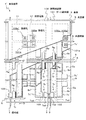
図2には第1実施形態の表示装置1の要部平面図を示し、図3には図2のA−A’断面図およびB−B’断面図を示す。以下、これらの図に基づいて表示装置1の層構成を説明する。尚、ここでは一例として150dpiの画素を想定し、一画素aが170μm角程度としたレイアウトの層構成を説明する。
図4には、上記表示装置1の製造工程図を示す。この製造工程図は、図2のA−A’断面に対応する図であり、以下図4と共に図2の平面図を参照して表示装置1の製造方法を説明する。尚、図2を用いたレイアウトの詳細な説明の重複は省略する。
ここでは、アクティブマトリックス型の表示装置における画素電極のスイッチング素子としてトップゲート型の薄膜トランジスタを用いた表示装置の構成を説明する。
第2実施形態の表示装置の回路構成は、第1実施形態において図1を用いて説明したと同様であって良く、ここでの重複する説明は省略する。
図5には第2実施形態の表示装置1’の要部平面図を示し、図6には図5のC−C’断面図およびD−D’断面図を示す。以下、これらの図に基づいて表示装置1’の層構成を説明する。尚、ここでは一例として150dpiの画素を想定し、一画素aが170μm角程度としたレイアウトの層構成を説明する。
図7には、上記表示装置1’の製造工程図を示す。この製造工程図は、図5のC−C’断面に対応する図であり、以下図7と共に図5の平面図を参照して表示装置1’の製造方法を説明する。尚、図5を用いたレイアウトの詳細な説明の重複は省略する。
Claims (11)
- 基板上に配列形成された画素電極スイッチング用の画素回路と、当該画素回路を覆う層間絶縁膜とを備えた表示装置において、
前記層間絶縁膜は、前記画素回路の接続部分を底部に露出させた接続孔を備え、
前記接続孔の底部には、前記画素回路のうち隣接する複数の画素回路の各接続部分が露出している
ことを特徴とする表示装置。 - 請求項1記載の表示装置において、
前記層間絶縁膜上には、前記接続孔の底部において前記各画素回路にそれぞれ独立して接続された複数の画素電極が配列している
ことを特徴とする表示装置。 - 請求項2記載の表示装置において、
前記隣接する複数の画素回路における前記画素電極との接続部分が、隣接する画素間の中央に配置されている
ことを特徴とする表示装置。 - 請求項1記載の表示装置において、
前記画素回路は、複数の走査線と複数の信号線との各交差部に配置され、
前記走査線の延設方向に隣接して配置された画素回路が、前記信号線に対して線対称にレイアウトされると共に、
前記接続孔が、前記走査線の延設方向に隣接して配置された複数の画素回路にまたがって配置されている
ことを特徴とする表示装置。 - 請求項1記載の表示装置において、
前記画素回路は、複数の走査線と複数の信号線との各交差部に配置され、
前記信号線の延設方向に隣接して配置された画素回路が、前記走査線に対して線対称にレイアウトされると共に、
前記接続孔が、前記信号線の延設方向に隣接して配置された複数の画素回路にまたがって配置されている
ことを特徴とする表示装置。 - 請求項1記載の表示装置において、
前記画素回路は、複数の走査線と複数の信号線との各交差部に配置され、
前記走査線の延設方向に隣接して配置された画素回路が、前記信号線に対して線対称にレイアウトされ、
前記信号線の延設方向に隣接して配置された画素回路が、前記走査線に対して線対称にレイアウトされると共に、
前記接続孔が、前記信号線の延方方向と前記走査線の延設方向とに隣接して配置された複数の画素回路にまたがって配置されている
ことを特徴とする表示装置。 - 請求項5,6のうちの1項に記載の表示装置において、
前記画素回路に接続される共通配線が、隣接して配置される2本の走査線間に配置された2つの画素回路で共有されている
ことを特徴とする表示装置。 - 請求項1記載の表示装置において、
前記層間絶縁膜は、有機材料で構成されている
ことを特徴とする表示装置。 - 基板上に画素電極スイッチング用の画素回路を配列形成する工程と、前記画素回路における接続部分を底部に露出させた接続孔を備えた層間絶縁膜を前記基板上に形成する工程とを行う表示装置の製造方法において、
前記接続孔の底部には、前記画素回路のうち隣接する複数の画素回路の各接続部分を露出させる
ことを特徴とする表示装置の製造方法。 - 請求項9記載の表示装置の製造方法において、
前記層間絶縁膜を形成した後、前記接続孔の底部において前記各画素回路にそれぞれ独立して接続された複数の画素電極を当該層間絶縁膜上に配列形成する
ことを特徴とする表示装置の製造方法。 - 請求項9記載の表示装置の製造方法において、
前記層間絶縁膜の形成は、印刷法を適用して行われる
ことを特徴とする表示装置の製造方法。
Priority Applications (4)
| Application Number | Priority Date | Filing Date | Title |
|---|---|---|---|
| JP2007177991A JP4389978B2 (ja) | 2007-07-06 | 2007-07-06 | 表示装置および表示装置の製造方法 |
| US12/144,747 US7786484B2 (en) | 2007-07-06 | 2008-06-24 | Display device having a portion of a pixel circuit exposed by a connection hole |
| KR1020080064846A KR20090004746A (ko) | 2007-07-06 | 2008-07-04 | 표시 장치 및 그 제조 방법 |
| CN2008101305482A CN101339343B (zh) | 2007-07-06 | 2008-07-07 | 显示装置及其制造方法 |
Applications Claiming Priority (1)
| Application Number | Priority Date | Filing Date | Title |
|---|---|---|---|
| JP2007177991A JP4389978B2 (ja) | 2007-07-06 | 2007-07-06 | 表示装置および表示装置の製造方法 |
Publications (2)
| Publication Number | Publication Date |
|---|---|
| JP2009015098A JP2009015098A (ja) | 2009-01-22 |
| JP4389978B2 true JP4389978B2 (ja) | 2009-12-24 |
Family
ID=40213441
Family Applications (1)
| Application Number | Title | Priority Date | Filing Date |
|---|---|---|---|
| JP2007177991A Expired - Fee Related JP4389978B2 (ja) | 2007-07-06 | 2007-07-06 | 表示装置および表示装置の製造方法 |
Country Status (4)
| Country | Link |
|---|---|
| US (1) | US7786484B2 (ja) |
| JP (1) | JP4389978B2 (ja) |
| KR (1) | KR20090004746A (ja) |
| CN (1) | CN101339343B (ja) |
Families Citing this family (9)
| Publication number | Priority date | Publication date | Assignee | Title |
|---|---|---|---|---|
| JP5251068B2 (ja) * | 2007-10-17 | 2013-07-31 | 株式会社リコー | アクティブマトリクス基板及び電子表示装置 |
| JP5376287B2 (ja) * | 2008-08-06 | 2013-12-25 | セイコーエプソン株式会社 | 回路基板、電気光学装置、電子機器 |
| CN103176652B (zh) * | 2013-03-08 | 2015-05-13 | 南昌欧菲光科技有限公司 | 触摸屏及其制造方法 |
| JP6225511B2 (ja) * | 2013-07-02 | 2017-11-08 | セイコーエプソン株式会社 | 表示装置及び電子機器 |
| KR101555753B1 (ko) * | 2013-11-18 | 2015-09-30 | 서울대학교산학협력단 | 단일 공정의 부식 방지된 구리 페이스트 제조와 다이폴 태그 안테나로의 응용 |
| CN104062821B (zh) * | 2014-06-05 | 2017-01-04 | 厦门天马微电子有限公司 | 一种薄膜晶体管阵列基板、显示面板和显示装置 |
| CN111357392A (zh) * | 2017-11-28 | 2020-06-30 | 堺显示器制品株式会社 | 有机el发光元件及其制造方法 |
| WO2021161528A1 (ja) * | 2020-02-14 | 2021-08-19 | シャープ株式会社 | 表示装置 |
| CN112711157B (zh) * | 2021-01-05 | 2023-11-28 | 武汉华星光电技术有限公司 | 一种阵列基板、阵列基板制程方法及显示面板 |
Family Cites Families (12)
| Publication number | Priority date | Publication date | Assignee | Title |
|---|---|---|---|---|
| SG54485A1 (en) * | 1996-03-29 | 1998-11-16 | Toshiba Kk | File managing method requiring a change in key data and ic card device using the method |
| US7308699B1 (en) * | 1998-09-15 | 2007-12-11 | Intel Corporation | Maintaining access to a video stack after an application crash |
| JP3683463B2 (ja) * | 1999-03-11 | 2005-08-17 | シャープ株式会社 | アクティブマトリクス基板、その製造方法、及び、該基板を用いたイメージセンサ |
| JP2001311960A (ja) | 2000-02-24 | 2001-11-09 | Seiko Epson Corp | 液晶装置及びこれを用いた電子機器 |
| JP3620490B2 (ja) | 2000-11-22 | 2005-02-16 | ソニー株式会社 | アクティブマトリクス型表示装置 |
| JP2002244576A (ja) | 2001-02-21 | 2002-08-30 | Sony Corp | 表示装置の製造方法、表示装置及び液晶表示装置 |
| JP2004334155A (ja) | 2002-09-30 | 2004-11-25 | Seiko Epson Corp | 電気光学装置および電子機器 |
| JP4590839B2 (ja) | 2003-08-01 | 2010-12-01 | ソニー株式会社 | 半導体基板、液晶表示装置及びプロジェクタ |
| KR101019045B1 (ko) * | 2003-11-25 | 2011-03-04 | 엘지디스플레이 주식회사 | 액정표시장치용 어레이기판과 그 제조방법 |
| JP4389737B2 (ja) * | 2004-09-22 | 2009-12-24 | セイコーエプソン株式会社 | 固体撮像装置及びその駆動方法 |
| KR101208724B1 (ko) * | 2005-01-03 | 2012-12-06 | 삼성디스플레이 주식회사 | 어레이 기판 및 이를 구비한 표시 패널 |
| JP5073194B2 (ja) | 2005-03-14 | 2012-11-14 | 株式会社リコー | フラットパネルディスプレイおよびその作製方法 |
-
2007
- 2007-07-06 JP JP2007177991A patent/JP4389978B2/ja not_active Expired - Fee Related
-
2008
- 2008-06-24 US US12/144,747 patent/US7786484B2/en not_active Expired - Fee Related
- 2008-07-04 KR KR1020080064846A patent/KR20090004746A/ko not_active Application Discontinuation
- 2008-07-07 CN CN2008101305482A patent/CN101339343B/zh not_active Expired - Fee Related
Also Published As
| Publication number | Publication date |
|---|---|
| CN101339343A (zh) | 2009-01-07 |
| CN101339343B (zh) | 2010-09-01 |
| KR20090004746A (ko) | 2009-01-12 |
| JP2009015098A (ja) | 2009-01-22 |
| US7786484B2 (en) | 2010-08-31 |
| US20090008713A1 (en) | 2009-01-08 |
Similar Documents
| Publication | Publication Date | Title |
|---|---|---|
| JP4389978B2 (ja) | 表示装置および表示装置の製造方法 | |
| JP5521270B2 (ja) | 薄膜トランジスタアレイ、薄膜トランジスタアレイの製造方法、および薄膜トランジスタアレイを用いたアクティブマトリクス型ディスプレイ | |
| US8598570B2 (en) | Organic transistor array, display device and method of fabricating display device | |
| US8258514B2 (en) | Semiconductor device and display apparatus using the semiconductor device | |
| JP2007281188A (ja) | トランジスタ、画素電極基板、電気光学装置、電子機器及び半導体素子の製造方法 | |
| US8642364B2 (en) | Thin film transistor structure, method of manufacturing the same, and electronic device | |
| JP6070073B2 (ja) | 薄膜トランジスタアレイ | |
| JP2009157069A (ja) | 薄膜トランジスタアレイ及びその製造方法 | |
| US20070295960A1 (en) | Semiconductor device, electro-optical device, electronic apparatus, and method of producing semiconductor device | |
| JP2007193267A (ja) | 薄膜トランジスタ装置及びその製造方法及び薄膜トランジスタアレイ及び薄膜トランジスタディスプレイ | |
| JP2007012669A (ja) | 薄膜トランジスタアレイとディスプレイ及び薄膜トランジスタアレイの製造方法 | |
| US9735381B2 (en) | Thin film transistor array and manufacturing method of the same | |
| US10629654B2 (en) | Thin film transistor array formed substrate, image display device substrate and manufacturing method of thin film transistor array formed substrate | |
| JP6331644B2 (ja) | 薄膜トランジスタアレイおよびその製造方法 | |
| WO2016208414A1 (ja) | 素子基板および素子基板の製造方法ならびに表示装置 | |
| JP2020088117A (ja) | 薄膜トランジスタアレイ基板、画像表示装置用基板、画像表示装置、およびこれらの製造方法 | |
| JP2005142277A (ja) | パターンの形成方法、電気光学装置の製造方法、デバイスの製造方法、電子機器 | |
| WO2014068916A1 (ja) | 薄膜トランジスタ | |
| JP2017203880A (ja) | 薄膜トランジスタアレイ、表示装置及び薄膜トランジスタアレイの製造方法 | |
| JP6627437B2 (ja) | 薄膜トランジスタアレイ基板の製造方法 | |
| JP2018182114A (ja) | 薄膜トランジスタアレイ、その製造方法、及び画像表示装置 |
Legal Events
| Date | Code | Title | Description |
|---|---|---|---|
| A977 | Report on retrieval |
Free format text: JAPANESE INTERMEDIATE CODE: A971007 Effective date: 20090626 |
|
| A131 | Notification of reasons for refusal |
Free format text: JAPANESE INTERMEDIATE CODE: A131 Effective date: 20090707 |
|
| A521 | Written amendment |
Free format text: JAPANESE INTERMEDIATE CODE: A523 Effective date: 20090820 |
|
| TRDD | Decision of grant or rejection written | ||
| A01 | Written decision to grant a patent or to grant a registration (utility model) |
Free format text: JAPANESE INTERMEDIATE CODE: A01 Effective date: 20090915 |
|
| A01 | Written decision to grant a patent or to grant a registration (utility model) |
Free format text: JAPANESE INTERMEDIATE CODE: A01 |
|
| A61 | First payment of annual fees (during grant procedure) |
Free format text: JAPANESE INTERMEDIATE CODE: A61 Effective date: 20090928 |
|
| FPAY | Renewal fee payment (event date is renewal date of database) |
Free format text: PAYMENT UNTIL: 20121016 Year of fee payment: 3 |
|
| FPAY | Renewal fee payment (event date is renewal date of database) |
Free format text: PAYMENT UNTIL: 20121016 Year of fee payment: 3 |
|
| FPAY | Renewal fee payment (event date is renewal date of database) |
Free format text: PAYMENT UNTIL: 20131016 Year of fee payment: 4 |
|
| R250 | Receipt of annual fees |
Free format text: JAPANESE INTERMEDIATE CODE: R250 |
|
| R250 | Receipt of annual fees |
Free format text: JAPANESE INTERMEDIATE CODE: R250 |
|
| LAPS | Cancellation because of no payment of annual fees |