JP4212552B2 - 半導体装置 - Google Patents
半導体装置 Download PDFInfo
- Publication number
- JP4212552B2 JP4212552B2 JP2004371056A JP2004371056A JP4212552B2 JP 4212552 B2 JP4212552 B2 JP 4212552B2 JP 2004371056 A JP2004371056 A JP 2004371056A JP 2004371056 A JP2004371056 A JP 2004371056A JP 4212552 B2 JP4212552 B2 JP 4212552B2
- Authority
- JP
- Japan
- Prior art keywords
- region
- semiconductor
- trench
- type
- gate
- Prior art date
- Legal status (The legal status is an assumption and is not a legal conclusion. Google has not performed a legal analysis and makes no representation as to the accuracy of the status listed.)
- Expired - Fee Related
Links
Images


Classifications
-
- H—ELECTRICITY
- H10—SEMICONDUCTOR DEVICES; ELECTRIC SOLID-STATE DEVICES NOT OTHERWISE PROVIDED FOR
- H10D—INORGANIC ELECTRIC SEMICONDUCTOR DEVICES
- H10D30/00—Field-effect transistors [FET]
- H10D30/60—Insulated-gate field-effect transistors [IGFET]
- H10D30/64—Double-diffused metal-oxide semiconductor [DMOS] FETs
- H10D30/66—Vertical DMOS [VDMOS] FETs
- H10D30/668—Vertical DMOS [VDMOS] FETs having trench gate electrodes, e.g. UMOS transistors
-
- H—ELECTRICITY
- H10—SEMICONDUCTOR DEVICES; ELECTRIC SOLID-STATE DEVICES NOT OTHERWISE PROVIDED FOR
- H10D—INORGANIC ELECTRIC SEMICONDUCTOR DEVICES
- H10D62/00—Semiconductor bodies, or regions thereof, of devices having potential barriers
- H10D62/10—Shapes, relative sizes or dispositions of the regions of the semiconductor bodies; Shapes of the semiconductor bodies
- H10D62/124—Shapes, relative sizes or dispositions of the regions of semiconductor bodies or of junctions between the regions
- H10D62/126—Top-view geometrical layouts of the regions or the junctions
- H10D62/127—Top-view geometrical layouts of the regions or the junctions of cellular field-effect devices, e.g. multicellular DMOS transistors or IGBTs
Landscapes
- Electrodes Of Semiconductors (AREA)
- Metal-Oxide And Bipolar Metal-Oxide Semiconductor Integrated Circuits (AREA)
Description
Claims (5)
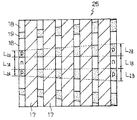
- 第1導電型の第1の半導体層と、
前記第1の半導体層上に設けられた第2導電型の第2の半導体層と、
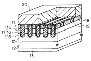
前記第2の半導体層を貫通して前記第1の半導体層に達するトレンチと、前記トレンチ内に絶縁膜を介して充填された導電材とを有するトレンチ・ゲートと、
前記第2の半導体層上に前記トレンチ・ゲートの前記導電材と前記絶縁膜を介して隣接形成された第1導電型の第3の半導体領域と、
前記第2の半導体層上に前記第3の半導体領域と前記トレンチ・ゲートに沿って交互に配置されるように隣接形成された第2導電型の第4の半導体領域とを具備し、
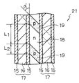
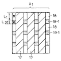
前記第3の半導体領域および前記第4の半導体領域は、前記トレンチ・ゲートの長手方向に対して傾きを持って配置されていることを特徴とする半導体装置。 - 請求項1記載の半導体装置において、
前記第3の半導体領域と前記第4の半導体領域との界面と前記トレンチ・ゲートの長手方向とが成す角度をαとしたとき、前記第3の半導体領域と前記第4の半導体領域は前記角度αが10〜75°の範囲となるように配置されていることを特徴とする半導体装置。 - 第1導電型の第1の半導体層と、
前記第1の半導体層上に設けられた第2導電型の第2の半導体層と、
前記第2の半導体層を貫通して前記第1の半導体層に達するトレンチと、前記トレンチ内に絶縁膜を介して充填された導電材とを有するトレンチ・ゲートと、
前記第2の半導体層上に前記トレンチ・ゲートの前記導電材と前記絶縁膜を介して隣接形成された第1導電型の第3の半導体領域と、
前記第2の半導体層上に前記第3の半導体領域と前記トレンチ・ゲートに沿って交互に配置されるように隣接形成された第2導電型の第4の半導体領域とを具備し、
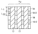
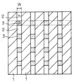
前記第4の半導体領域は、実効素子領域における前記第4の半導体領域の占める割合が、駆動電圧が印加されるゲート信号入力端子領域に近い領域より遠い領域の方が大きくなるように形成されていることを特徴とする半導体装置。 - 第1導電型の第1の半導体層と、
前記第1の半導体層上に設けられた第2導電型の第2の半導体層と、
前記第2の半導体層を貫通して前記第1の半導体層に達するトレンチと、前記トレンチ内に絶縁膜を介して充填された導電材とを有するトレンチ・ゲートと、
前記第2の半導体層上に前記トレンチ・ゲートの前記導電材と前記絶縁膜を介して隣接形成された第1導電型の第3の半導体領域と、
前記第2の半導体層上に前記第3の半導体領域と前記トレンチ・ゲートに沿って交互に配置されるように隣接形成された第2導電型の第4の半導体領域とを具備し、
前記第3の半導体領域および前記第4の半導体領域は少なくとも一部が前記トレンチ・ゲートの長手方向に対して傾きを持って配置されており、かつ前記第4の半導体領域は実効素子領域における前記第4の半導体領域の占める割合が、駆動電圧が印加されるゲート信号入力端子領域に近い領域より遠い領域の方が大きくなるように形成されていることを特徴とする半導体装置。 - 請求項3または請求項4記載の半導体装置において、
前記第3の半導体領域が前記トレンチ・ゲートと接する部分の長さをL1、前記第4の半導体領域が前記トレンチ・ゲートと接する部分の長さをL2、これらの長さ比をL2/L1としたとき、前記第4の半導体領域は前記入力端子領域に近い領域から前記入力端子領域から遠い領域に向けて、前記長さ比L2/L1が連続的に増加するように形成されていることを特徴とする半導体装置。
Priority Applications (2)
| Application Number | Priority Date | Filing Date | Title |
|---|---|---|---|
| JP2004371056A JP4212552B2 (ja) | 2004-12-22 | 2004-12-22 | 半導体装置 |
| US11/305,202 US7400007B2 (en) | 2004-12-22 | 2005-12-19 | Semiconductor device |
Applications Claiming Priority (1)
| Application Number | Priority Date | Filing Date | Title |
|---|---|---|---|
| JP2004371056A JP4212552B2 (ja) | 2004-12-22 | 2004-12-22 | 半導体装置 |
Publications (2)
| Publication Number | Publication Date |
|---|---|
| JP2006179664A JP2006179664A (ja) | 2006-07-06 |
| JP4212552B2 true JP4212552B2 (ja) | 2009-01-21 |
Family
ID=36683002
Family Applications (1)
| Application Number | Title | Priority Date | Filing Date |
|---|---|---|---|
| JP2004371056A Expired - Fee Related JP4212552B2 (ja) | 2004-12-22 | 2004-12-22 | 半導体装置 |
Country Status (2)
| Country | Link |
|---|---|
| US (1) | US7400007B2 (ja) |
| JP (1) | JP4212552B2 (ja) |
Families Citing this family (4)
| Publication number | Priority date | Publication date | Assignee | Title |
|---|---|---|---|---|
| US8084909B2 (en) * | 2009-04-09 | 2011-12-27 | Goodzeit Carl L | Dual armature motor/generator with flux linkage |
| WO2012017878A1 (ja) * | 2010-08-02 | 2012-02-09 | 日産自動車株式会社 | 半導体装置 |
| CN104995737B (zh) * | 2013-02-13 | 2017-10-27 | 丰田自动车株式会社 | 半导体装置 |
| CN116110962B (zh) * | 2023-04-03 | 2025-10-24 | 重庆云潼科技有限公司 | 一种高抗短路能力的载流子存储沟槽栅igbt器件 |
Family Cites Families (5)
| Publication number | Priority date | Publication date | Assignee | Title |
|---|---|---|---|---|
| US5448083A (en) * | 1991-08-08 | 1995-09-05 | Kabushiki Kaisha Toshiba | Insulated-gate semiconductor device |
| DE69233105T2 (de) * | 1991-08-08 | 2004-05-06 | Kabushiki Kaisha Toshiba, Kawasaki | Bipolartransistor mit isoliertem Graben-Gate |
| JP3384198B2 (ja) * | 1995-07-21 | 2003-03-10 | 三菱電機株式会社 | 絶縁ゲート型半導体装置およびその製造方法 |
| JP3329707B2 (ja) * | 1997-09-30 | 2002-09-30 | 株式会社東芝 | 半導体装置 |
| JP4421144B2 (ja) * | 2001-06-29 | 2010-02-24 | 株式会社東芝 | 半導体装置 |
-
2004
- 2004-12-22 JP JP2004371056A patent/JP4212552B2/ja not_active Expired - Fee Related
-
2005
- 2005-12-19 US US11/305,202 patent/US7400007B2/en not_active Expired - Fee Related
Also Published As
| Publication number | Publication date |
|---|---|
| JP2006179664A (ja) | 2006-07-06 |
| US20060157778A1 (en) | 2006-07-20 |
| US7400007B2 (en) | 2008-07-15 |
Similar Documents
| Publication | Publication Date | Title |
|---|---|---|
| JP4967236B2 (ja) | 半導体素子 | |
| US9024382B2 (en) | Semiconductor device | |
| JP6323556B2 (ja) | 半導体装置 | |
| WO2014163058A1 (ja) | 半導体装置 | |
| JP2015213141A (ja) | 縦型半導体装置およびその製造方法 | |
| JP5297706B2 (ja) | 半導体装置 | |
| WO2013179648A1 (ja) | 半導体装置 | |
| CN104465718B (zh) | 半导体装置 | |
| JP5652409B2 (ja) | 半導体素子 | |
| JP6183550B2 (ja) | 半導体装置 | |
| JP2008277352A (ja) | 半導体装置 | |
| CN107731892A (zh) | 半导体装置 | |
| JP7256771B2 (ja) | 半導体装置 | |
| JP2004241768A (ja) | 半導体素子 | |
| JP2006245477A (ja) | 半導体装置 | |
| JP5217158B2 (ja) | 半導体装置 | |
| JP4212552B2 (ja) | 半導体装置 | |
| JP2016096307A (ja) | 半導体装置 | |
| JP2005150348A (ja) | 半導体装置 | |
| JP2012099696A (ja) | 半導体装置 | |
| JP7387501B2 (ja) | 半導体装置およびその制御方法 | |
| JP6177300B2 (ja) | 半導体装置 | |
| JP6089070B2 (ja) | 半導体装置 | |
| JP2009071082A (ja) | 半導体装置 | |
| JP2025090230A (ja) | 半導体装置 |
Legal Events
| Date | Code | Title | Description |
|---|---|---|---|
| A977 | Report on retrieval |
Free format text: JAPANESE INTERMEDIATE CODE: A971007 Effective date: 20081009 |
|
| TRDD | Decision of grant or rejection written | ||
| A01 | Written decision to grant a patent or to grant a registration (utility model) |
Free format text: JAPANESE INTERMEDIATE CODE: A01 Effective date: 20081021 |
|
| A01 | Written decision to grant a patent or to grant a registration (utility model) |
Free format text: JAPANESE INTERMEDIATE CODE: A01 |
|
| A61 | First payment of annual fees (during grant procedure) |
Free format text: JAPANESE INTERMEDIATE CODE: A61 Effective date: 20081028 |
|
| FPAY | Renewal fee payment (event date is renewal date of database) |
Free format text: PAYMENT UNTIL: 20111107 Year of fee payment: 3 |
|
| FPAY | Renewal fee payment (event date is renewal date of database) |
Free format text: PAYMENT UNTIL: 20111107 Year of fee payment: 3 |
|
| FPAY | Renewal fee payment (event date is renewal date of database) |
Free format text: PAYMENT UNTIL: 20121107 Year of fee payment: 4 |
|
| FPAY | Renewal fee payment (event date is renewal date of database) |
Free format text: PAYMENT UNTIL: 20131107 Year of fee payment: 5 |
|
| R250 | Receipt of annual fees |
Free format text: JAPANESE INTERMEDIATE CODE: R250 |
|
| LAPS | Cancellation because of no payment of annual fees |