JP4212552B2 - Semiconductor device - Google Patents
Semiconductor device Download PDFInfo
- Publication number
- JP4212552B2 JP4212552B2 JP2004371056A JP2004371056A JP4212552B2 JP 4212552 B2 JP4212552 B2 JP 4212552B2 JP 2004371056 A JP2004371056 A JP 2004371056A JP 2004371056 A JP2004371056 A JP 2004371056A JP 4212552 B2 JP4212552 B2 JP 4212552B2
- Authority
- JP
- Japan
- Prior art keywords
- region
- semiconductor
- trench
- type
- gate
- Prior art date
- Legal status (The legal status is an assumption and is not a legal conclusion. Google has not performed a legal analysis and makes no representation as to the accuracy of the status listed.)
- Expired - Fee Related
Links
Images


Classifications
-
- H—ELECTRICITY
- H10—SEMICONDUCTOR DEVICES; ELECTRIC SOLID-STATE DEVICES NOT OTHERWISE PROVIDED FOR
- H10D—INORGANIC ELECTRIC SEMICONDUCTOR DEVICES
- H10D30/00—Field-effect transistors [FET]
- H10D30/60—Insulated-gate field-effect transistors [IGFET]
- H10D30/64—Double-diffused metal-oxide semiconductor [DMOS] FETs
- H10D30/66—Vertical DMOS [VDMOS] FETs
- H10D30/668—Vertical DMOS [VDMOS] FETs having trench gate electrodes, e.g. UMOS transistors
-
- H—ELECTRICITY
- H10—SEMICONDUCTOR DEVICES; ELECTRIC SOLID-STATE DEVICES NOT OTHERWISE PROVIDED FOR
- H10D—INORGANIC ELECTRIC SEMICONDUCTOR DEVICES
- H10D62/00—Semiconductor bodies, or regions thereof, of devices having potential barriers
- H10D62/10—Shapes, relative sizes or dispositions of the regions of the semiconductor bodies; Shapes of the semiconductor bodies
- H10D62/124—Shapes, relative sizes or dispositions of the regions of semiconductor bodies or of junctions between the regions
- H10D62/126—Top-view geometrical layouts of the regions or the junctions
- H10D62/127—Top-view geometrical layouts of the regions or the junctions of cellular field-effect devices, e.g. multicellular DMOS transistors or IGBTs
Landscapes
- Electrodes Of Semiconductors (AREA)
- Metal-Oxide And Bipolar Metal-Oxide Semiconductor Integrated Circuits (AREA)
Description
本発明は半導体装置に係り、特に縦型MOS(Metal-Oxide-Semiconductor)ゲート構造を有する半導体装置に関する。 The present invention relates to a semiconductor device, and more particularly to a semiconductor device having a vertical MOS (Metal-Oxide-Semiconductor) gate structure.
半導体上方にトレンチ(trench:溝)を形成し、これを利用したトレンチ・ゲート構造は、IGBT(Insulated Gate Bipolar Transistor)やMOS−FET(Metal Oxide Semiconductor - Field Effect Transistor)等の半導体素子に応用されており、特に電力用途等に有利な構造である。例えば、トレンチ・ゲート構造を有するMOSFETはスイッチング速度が速く、また電流容量が大きく、数10V〜300V程度の耐圧が得られるため、携帯型端末やパーソナル・コンピュータ等のスイッチング電源等に利用されつつある。 A trench (trench) is formed above the semiconductor, and the trench gate structure using this is applied to semiconductor elements such as IGBT (Insulated Gate Bipolar Transistor) and MOS-FET (Metal Oxide Semiconductor-Field Effect Transistor). In particular, this structure is advantageous for power applications. For example, a MOSFET having a trench gate structure has a high switching speed, a large current capacity, and a withstand voltage of about several tens of volts to 300 volts, so that it is being used as a switching power source for portable terminals and personal computers. .
このようなトレンチ・ゲート構造を有するパワー半導体装置について、nチャネル型トレンチMOSFETを一例として説明する。トレンチMOSFETにおいて、例えばn型ドリフト層とp型ベース層とが積層形成された半導体ウェーハに、p型ベース層を貫通してn型ドリフト層に達するトレンチが形成される。トレンチ内にはゲート絶縁膜を介してゲート電極材が形成され、これらによりトレンチ・ゲートが構成される。n型ドリフト層の裏面側にはn+型ドレイン領域を介してドレイン電極が形成される。 A power semiconductor device having such a trench-gate structure will be described using an n-channel trench MOSFET as an example. In the trench MOSFET, for example, a trench reaching the n-type drift layer through the p-type base layer is formed in a semiconductor wafer in which an n-type drift layer and a p-type base layer are stacked. A gate electrode material is formed in the trench with a gate insulating film interposed therebetween, thereby forming a trench gate. A drain electrode is formed on the back side of the n-type drift layer via an n + -type drain region.
一方、p型ベース層の上にはn+型ソース領域とこれに隣接して形成されたp+型領域とが設けられる。さらに、これらの上部にはソース電極が形成される。従来のMOSFETにおいては、例えば図8に示すように、トレンチ・ゲート1に隣接させたn+型ソース領域2をそれぞれトレンチの形成方向(奥行き方向)に沿って形成し、さらにこれらn+型ソース領域2間にp+型領域3を形成した構造が一般的に採用されている(例えば特許文献1の図6参照)。しかし、このような構造ではトレンチ間隔がn+型ソース領域2とp+型領域3の幅に規制されることから、トレンチ間隔の狭小化に限界がある。
On the other hand, an n + type source region and a p + type region formed adjacent thereto are provided on the p type base layer. Further, a source electrode is formed on these. In the conventional MOSFET, for example, as shown in FIG. 8, n + -
一方、微細化技術の進歩に伴って、トレンチ間距離Wは1μm以下とすることが可能になっている。そこで、例えば図9に示すように、トレンチ・ゲート1間にn+型ソース領域2とp+型領域3とをトレンチの形成方向に沿って交互に隣接配置した構造、言い換えるとトレンチ・ゲート1と、交互に配置したn+型ソース領域2およびp+型領域3とを直交させた構造が提案されている。例えば、特許文献2には上記したような素子上部構造を適用したIGBTが記載されている。また、特許文献3にはトレンチ・ゲートに沿ったソース領域からインジェクタ領域までの長さが、これらの間の最短距離より長くなるようにトレンチ・ゲートを配置した素子構造が記載されている。
On the other hand, with the progress of miniaturization technology, the inter-trench distance W can be set to 1 μm or less. Therefore, for example, as shown in FIG. 9, a structure in which n + -
上述したような素子上部構造(図9)を適用したパワーMOSFETにおいては、ゲート電極材に所定の電圧を印加すると、p型ベース層のうちのゲート絶縁膜に隣接した領域に反転層が形成され、ソース電極とドレイン電極との間でオン状態が形成される。このようなパワーMOSFETではトレンチ間隔を微細化することによって、素子実効面積に占める電流通路(チャネル)の割合を増加させることができる。従って、パワーMOSFETのオン状態での抵抗を低減することが可能となる。
しかしながら、図9に示したn+型ソース領域2とp+型領域3の配置構造において、オン抵抗を低減するためにはトレンチ・ゲート1間の素子領域に対するn+型ソース領域2が占める割合を大きくする必要がある。このときの最も大きな問題点としてはアバランシェ破壊が挙げられる。これは、インダクタンス負荷駆動直後にパワーMOSFETがオンからオフに移行する際に生じるブレイクダウン電流によって、任意のセルにおけるp型ベース層で大きく電圧降下が発生することに起因する。
However, in the arrangement structure of the n + -
すなわち、n+型ソース領域/p型ベース層/n型ドリフト層からなる寄生npnバイポーラトランジスタがオンすると大電流が流れる。この寄生バイポーラトランジスタが動作したセルは、動作しないセルと比較して耐圧が低下するため、電流はこのセルに集中して流れることになり、デバイス破壊に至る。図9に示した素子上部構造において、n+型ソース領域2の幅を広くするということは、チャネル近傍でブレイクダウンが生じた際に、p型ベース層を流れるホール電流がp+型領域3に流れ込むまでの道のりに高い抵抗が配置されていることに等しい。この抵抗が大きいと寄生npnバイポーラトランジスタがオンしやすくなり、その結果としてアバランシェ破壊に至りやすい。
That is, a large current flows when a parasitic npn bipolar transistor comprising n + type source region / p type base layer / n type drift layer is turned on. A cell in which the parasitic bipolar transistor is operated has a lower breakdown voltage than a cell that does not operate, so that current flows in a concentrated manner in the cell, resulting in device destruction. In the device upper structure shown in FIG. 9, increasing the width of the n + -
本発明はこのような課題に対処するためになされたものであって、縦型MOSゲート構造(トレンチ・ゲート構造)を有する半導体装置の素子上部構造に基づくオン抵抗の低減効果を阻害することなく、アバランシェ耐量を高めることを可能にした半導体装置を提供することを目的としている。 The present invention has been made to cope with such a problem, and does not hinder the on-resistance reduction effect based on the element upper structure of a semiconductor device having a vertical MOS gate structure (trench gate structure). An object of the present invention is to provide a semiconductor device capable of increasing the avalanche resistance.
本発明の一態様に係る半導体装置は、第1導電型の第1の半導体層と、前記第1の半導体層上に設けられた第2導電型の第2の半導体層と、前記第2の半導体層を貫通して前記第1の半導体層に達するトレンチと、前記トレンチ内に絶縁膜を介して充填された導電材とを有するトレンチ・ゲートと、前記第2の半導体層上に前記トレンチ・ゲートの前記導電材と前記絶縁膜を介して隣接形成された第1導電型の第3の半導体領域と、前記第2の半導体層上に前記第3の半導体領域と前記トレンチ・ゲートに沿って交互に配置されるように隣接形成された第2導電型の第4の半導体領域とを具備し、前記第3の半導体領域および前記第4の半導体領域は、前記トレンチ・ゲートの長手方向に対して傾きを持って交差するように配置されていることを特徴している。 A semiconductor device according to one embodiment of the present invention includes a first conductive type first semiconductor layer, a second conductive type second semiconductor layer provided over the first semiconductor layer, and the second conductive type. A trench gate having a trench penetrating the semiconductor layer and reaching the first semiconductor layer; a conductive material filled in the trench through an insulating film; and the trench gate on the second semiconductor layer. A third semiconductor region of a first conductivity type formed adjacent to the conductive material of the gate via the insulating film; and the third semiconductor region on the second semiconductor layer along the trench gate A fourth semiconductor region of the second conductivity type adjacently formed so as to be alternately arranged, and the third semiconductor region and the fourth semiconductor region are arranged in a longitudinal direction of the trench gate. Placed so that they intersect with an inclination. It has been characterized.
本発明の他の態様に係る半導体装置は、第1導電型の第1の半導体層と、前記第1の半導体層上に設けられた第2導電型の第2の半導体層と、前記第2の半導体層を貫通して前記第1の半導体層に達するトレンチと、前記トレンチ内に絶縁膜を介して充填された導電材とを有するトレンチ・ゲートと、前記第2の半導体層上に前記トレンチ・ゲートの前記導電材と前記絶縁膜を介して隣接形成された第1導電型の第3の半導体領域と、前記第2の半導体層上に前記第3の半導体領域と前記トレンチ・ゲートに沿って交互に配置されるように隣接形成された第2導電型の第4の半導体領域とを具備し、前記第4の半導体領域は、実効素子領域における前記第4の半導体領域の占める割合が、駆動電圧が印加されるゲート信号入力端子領域に近い領域より遠い領域の方が大きくなるように形成されていることを特徴としている。 A semiconductor device according to another aspect of the present invention includes a first conductive type first semiconductor layer, a second conductive type second semiconductor layer provided on the first semiconductor layer, and the second conductive type. A trench gate having a trench reaching the first semiconductor layer through the semiconductor layer, a conductive material filled in the trench through an insulating film, and the trench on the second semiconductor layer A third semiconductor region of the first conductivity type formed adjacent to the conductive material of the gate via the insulating film, and along the third semiconductor region and the trench gate on the second semiconductor layer; And a fourth semiconductor region of the second conductivity type adjacently formed so as to be alternately arranged, and the fourth semiconductor region has a ratio of the fourth semiconductor region in the effective element region, Close to the gate signal input terminal area where the drive voltage is applied Is characterized in that towards the farther than frequency region is formed to be larger.
本発明のさらに他の態様に係る半導体装置は、第1導電型の第1の半導体層と、前記第1の半導体層上に設けられた第2導電型の第2の半導体層と、前記第2の半導体層を貫通して前記第1の半導体層に達するトレンチと、前記トレンチ内に絶縁膜を介して充填された導電材とを有するトレンチ・ゲートと、前記第2の半導体層上に前記トレンチ・ゲートの前記導電材と前記絶縁膜を介して隣接形成された第1導電型の第3の半導体領域と、前記第2の半導体層上に前記第3の半導体領域と前記トレンチ・ゲートに沿って交互に配置されるように隣接形成された第2導電型の第4の半導体領域とを具備し、前記第3の半導体領域および前記第4の半導体領域は少なくとも一部が前記トレンチ・ゲートの長手方向に対して傾きを持って交差するように配置されており、かつ前記第4の半導体領域は実効素子領域における前記第4の半導体領域の占める割合が、駆動電圧が印加されるゲート信号入力端子領域に近い領域より遠い領域の方が大きくなるように形成されていることを特徴としている。 A semiconductor device according to still another aspect of the present invention includes a first conductivity type first semiconductor layer, a second conductivity type second semiconductor layer provided on the first semiconductor layer, and the first conductivity type. A trench gate having a trench reaching the first semiconductor layer through the two semiconductor layers, a conductive material filled in the trench through an insulating film, and the trench on the second semiconductor layer. A third semiconductor region of a first conductivity type formed adjacent to the conductive material of the trench gate via the insulating film; and the third semiconductor region and the trench gate on the second semiconductor layer. And a fourth semiconductor region of a second conductivity type adjacently formed so as to be alternately disposed along the trench, at least a part of the third semiconductor region and the fourth semiconductor region being the trench gate Intersect with the longitudinal direction of The ratio of the fourth semiconductor region in the effective element region to the fourth semiconductor region is larger in the region farther than the region close to the gate signal input terminal region to which the drive voltage is applied. It is characterized by being formed.
本発明の一態様に係る半導体装置は、第3の半導体領域および第4の半導体領域をトレンチ・ゲートの長手方向に対して傾きを持って交差させているため、ブレイクダウン電流に対する第3の半導体領域直下のもぐり抵抗を低減することができる。これによって、寄生npnバイポーラトランジスタの駆動が抑制されることから、オン抵抗の低減効果を阻害することなく、アバランシェ耐量を高めることが可能となる。 In the semiconductor device according to one embodiment of the present invention, since the third semiconductor region and the fourth semiconductor region intersect with each other with an inclination with respect to the longitudinal direction of the trench gate, the third semiconductor against the breakdown current The drilling resistance directly under the region can be reduced. As a result, the driving of the parasitic npn bipolar transistor is suppressed, so that the avalanche resistance can be increased without hindering the effect of reducing the on-resistance.
本発明の他の態様に係る半導体装置は、実効素子領域における第4の半導体領域の占める割合をゲート信号入力端子領域に近い領域より遠い領域の方が大きくなるように設定しているため、オン抵抗の低減効果を損なうことなく、オフタイミングのずれ等により電流が集中しやすい領域(ゲート信号入力端子領域から遠い領域)のアバランシェ耐量を高めることが可能となる。 In the semiconductor device according to another aspect of the present invention, the proportion of the fourth semiconductor region in the effective element region is set so that the region far from the region close to the gate signal input terminal region is larger. Without impairing the effect of reducing the resistance, it is possible to increase the avalanche resistance in a region where current is likely to concentrate due to a shift in off timing or the like (region far from the gate signal input terminal region).
本発明のさらに他の態様に係る半導体装置によれば、寄生npnバイポーラトランジスタの駆動を抑制すると共に、電流集中に対する耐性を高めることによって、オン抵抗の低減効果を損なうことなく、アバランシェ耐量を高めることが可能となる。 According to the semiconductor device according to still another aspect of the present invention, it is possible to increase the avalanche resistance without impairing the on-resistance reduction effect by suppressing the driving of the parasitic npn bipolar transistor and increasing the resistance against current concentration. Is possible.
以下、本発明を実施するための形態について、図面を参照して説明する。なお、以下では本発明の実施形態を図面に基づいて述べるが、それらの図面は図解のみの目的のために提供されるものであり、本発明はそれらの図面に限定するものではない。 Hereinafter, embodiments for carrying out the present invention will be described with reference to the drawings. In the following, embodiments of the present invention will be described with reference to the drawings. However, the drawings are provided for the purpose of illustration only, and the present invention is not limited to the drawings.
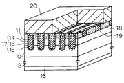
まず図1を参照して、本発明の実施形態による半導体装置の基本構造について述べる。図1は本発明の半導体装置を適用したnチャネル型トレンチMOSFETの要部基本構造を一部断面で示す斜視図である。なお、図1は半導体ウェーハ上に並列形成された複数の素子単位のうちの一部を抜き出して斜め上方から眺めた斜視図であって、MOSFET表面の配置を理解しやすいようにソース電極の一部を取り除いた状態を示している。 First, a basic structure of a semiconductor device according to an embodiment of the present invention will be described with reference to FIG. FIG. 1 is a perspective view, partially in section, showing a basic structure of a main part of an n-channel trench MOSFET to which a semiconductor device of the present invention is applied. FIG. 1 is a perspective view of a part of a plurality of element units formed in parallel on a semiconductor wafer and viewed from obliquely above, and shows a source electrode so that the arrangement of the MOSFET surface can be easily understood. The part is removed.
図1において、10はn型ドリフト層であり、このn型ドリフト層10上にはp型ベース層11が積層形成されている。n型ドリフト層10の下側にはn+型ドレイン領域12が存在しており、その裏面側にはドレイン電極13が形成されている。なお、これらの構造は、例えばn+型半導体ウェーハ(12)上にn-型層(n型ドリフト層10)とp型層(p型ベース層11)とを順に積層形成することにより作製される。
In FIG. 1,
上記したn型ドリフト層10やp型ベース層11を有する半導体ウェーハの表面側には、p型ベース層11を貫通してn型ドリフト層10に達するトレンチ14が形成されている。トレンチ14内には、その内壁面に形成されたゲート絶縁膜15を介してゲート電極材16が充填されており、これらによりトレンチ・ゲート17が構成されている。ゲート電極材17には、例えばポリシリコンのような導電材が用いられる。
A
一方、p型ベース層11上にはn+型ソース領域18とp+型領域19とが形成されている。これらn+型ソース領域18とp+型領域19は、トレンチ・ゲート17間の素子領域内に形成されており、さらにトレンチ・ゲート17の長手方向(トレンチ14の形成方向/図中奥行き方向)に沿って交互に隣接して配置されている。n+型ソース領域18はトレンチ・ゲート17のゲート電極材16とゲート絶縁膜15を介して隣接している。さらに、n+型ソース領域18およびp+型領域19の上部には、これらと接続するソース電極20が形成されている。
On the other hand, an n +
上述したトレンチ・ゲート17は、例えば以下のようにして作製される。まず、素子上面に一方向のトレンチ14を並行に形成する。トレンチ14の内壁面にゲート絶縁膜15を形成した後、ゲート電極材16を充填し、さらにゲート電極材16の上部もゲート絶縁膜15で覆うことによって、トレンチ・ゲート17を作製する。次いで、p型ベース層11上にトレンチ・ゲート17と交差するように、n+型ソース領域18となる領域とp+型領域19となる領域を、それぞれストライプ状に交互に隣接させて形成する。なお、各ストライプ領域はトレンチ・ゲート17で分断されることで、トレンチ・ゲート17間の素子領域に交互に隣接形成されたn+型ソース領域18およびp+型領域19となる。
The above-described
このような素子構造を有するパワーMOSFETにおいて、ゲート電極材16に所定の電圧を印加すると、p型ベース層11のうちのゲート絶縁膜15に隣接した領域に反転層が形成され、ソース電極20とドレイン電極13との間でオン状態が形成される。また、パワーMOSFETのオンからオフへの移行時にチャネル近傍でブレイクダウンが生じた際に、p型ベース層11を流れるホール電流はp+型領域19に流れ込む。
In a power MOSFET having such an element structure, when a predetermined voltage is applied to the
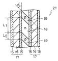
本発明の半導体装置を適用した第1の実施形態によるパワーMOSFETは、上述した基本構造(図1に示したトレンチ・ゲート構造を有するMOSFETの基本構造)を有し、かつ図2および図3に示すように、n+型ソース領域18とp+型領域19とがトレンチ・ゲート17の長手方向に対して傾きを持って交差するように配置されている。図2は第1の実施形態によるパワーMOSFET21の素子上部構造(ソース電極20を取り除いた部分の構造)を示す平面図であり、図3はパワーMOSFET21のトレンチ・ゲート17とn+型ソース領域18およびp+型領域19とが存在する部分を平面方向(横方向)に切断した要部拡大断面図である。
The power MOSFET according to the first embodiment to which the semiconductor device of the present invention is applied has the basic structure described above (the basic structure of the MOSFET having the trench-gate structure shown in FIG. 1), and FIGS. As shown, the n +
すなわち、トレンチ・ゲート17はn+型ソース領域18およびp+型領域19の形成方向に対して角度αを持って交差するように配置されている。n+型ソース領域18およびp+型領域19の形成方向とは、上述したようにトレンチ14を形成する前の状態における各ストライプ領域の形成方向を示すものであり、このn+型ソース領域18およびp+型領域19の形成方向に対してトレンチ・ゲート17の長手方向(トレンチ14の形成方向)は角度αで示される傾きを持って交差している。言い換えると、n+型ソース領域18とp+型領域19との界面は、トレンチ・ゲート17の長手方向に対して角度αだけ傾いた状態で配置されている。
That is, the
上記したように、n+型ソース領域18およびp+型領域19をトレンチ・ゲート17の長手方向に対して傾きを持って交差するように配置することによって、n+型ソース領域18の下部に位置するp型ベース層11の各部からp+型領域19までの距離を短縮することができる。このp型ベース層11からp+型領域19までの距離の短縮は、チャネル近傍で生じたブレイクダウン電流に対するn+型ソース領域18直下のもぐり抵抗が低減されることを意味する。このように、n+型ソース領域18直下のもぐり抵抗を低減することで、前述した寄生npnバイポーラトランジスタの駆動に基づく電流集中が低減されることから、寄生npnバイポーラトランジスタの駆動に起因するアバランシェ破壊の発生を抑制することが可能となる。
As described above, the n + -
このようなn+型ソース領域18およびp+型領域19の斜め配置に基づくアバランシェ耐量の向上効果は、図3に示すn+型ソース領域18の基準長さ(トレンチ・ゲート17と接する部分の長さ)L1とp+型領域19の基準長さ(トレンチ・ゲート17と接する部分の長さ)L2との比率を、従来の直交構造と同一とした上で実現される。従って、トレンチ間距離Wを一定とした場合、トレンチ・ゲート17間の素子領域に対してn+型ソース領域18が占める割合を維持してオン抵抗の低減を図った上で、アバランシェ耐量を高めることができる。これによって、トレンチ・ゲート構造を有するパワーMOSFET21の実用性や信頼性等を向上させることが可能となる。なお、L1とL2との比率は任意に設定可能であり、例えばL1:L2=2:1〜5:1の範囲とされる。
The effect of improving the avalanche resistance based on the oblique arrangement of the n +
上述したn+型ソース領域18およびp+型領域19の形成方向とトレンチ・ゲート17の長手方向とが成す角度αは、従来の直交構造に対してもぐり抵抗の低減効果が得られる範囲で任意に設定可能である。半導体製造技術におけるマスクアラインメントの精度は±1°以下であるため、このようなアラインメント精度を超える範囲で角度αを設定することができる。ただし、角度αが大きすぎると従来の直交構造と比較した場合のアバランシェ耐量の向上効果が不十分となるため、角度αは75°以下とすることが好ましい。一方、角度αが小さすぎると各領域18、19の形状が不安定になり、特性の低下等を招くおそれがあるため、角度αは10°以上とすることが好ましい。
The angle α formed by the formation direction of the n + -
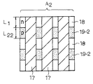
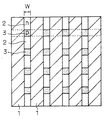
次に、本発明の第2の実施形態による半導体装置について説明する。本発明の半導体装置を適用した第2の実施形態によるパワーMOSFETは、上述した基本構造(図1に示したトレンチ・ゲート構造を有するMOSFETの基本構造)を有し、かつ図4ないし図6に示すように、実効素子領域におけるp+型領域19の占める割合に基づいて複数の領域A1、A2が設定されている。図4は第2の実施形態によるパワーMOSFET22の平面図である。図4において、23はゲート電極、24は駆動電圧が印加されるゲート信号入力端子領域である。すなわち、ゲート電極23には領域24に接続された外部端子からゲート信号が入力され、パワーMOSFET22のオン・オフ動作が制御される。
Next, a semiconductor device according to a second embodiment of the present invention will be described. The power MOSFET according to the second embodiment to which the semiconductor device of the present invention is applied has the basic structure described above (the basic structure of the MOSFET having the trench-gate structure shown in FIG. 1), and FIGS. As shown, a plurality of regions A 1 and A 2 are set based on the proportion of the p + -
ここで、アバランシェ破壊に至る原因は、前述した寄生npnバイポーラトランジスタの駆動に起因する場合に加えて、パワーMOSFETのゲートが不均一にオフすることに起因する場合が考えられる。つまり、ゲートがオンしている状態ではチャネルに電流が流れているが、ゲート信号入力端子領域24にオフの信号が入ったとき、ゲート信号入力端子領域24に近いセルと遠いセルとではオフのタイミングにずれが生じる場合がある。これはメタル層とポリシリコン等の導電材からなるゲート電位のネットワークが、ゲート信号入力端子領域24から遠い部分でゲート抵抗の増加により遅延が生じるためである。
Here, the cause of the avalanche breakdown can be attributed to the case where the gate of the power MOSFET is turned off non-uniformly in addition to the case where the parasitic npn bipolar transistor is driven. In other words, a current flows through the channel when the gate is on, but when an off signal is input to the gate signal
インダクタンス負荷駆動直後のオンからオフへの過渡状態において、ゲート抵抗の増加に基づく遅延が生じると、オフしているセルとオンしているセルとが同時に存在することとなる。この場合、遅れてオフしたセルにブレイクダウン電流が集中し、アバランシェ破壊に至りやすい。このような理由でゲート信号入力端子領域24から遠いセルでは電流集中が生じやすい。ゲート信号入力端子領域24からの距離に基づくオフ時の電流集中を抑制してアバランシェ破壊を防ぐためには、ゲート電位のネットワークの抵抗を低減し、パワーMOSFET全体を均一にオン・オフさせることが考えられる。
In the transient state from on to off immediately after the inductance load is driven, if a delay occurs due to an increase in the gate resistance, an off cell and an on cell exist at the same time. In this case, the breakdown current concentrates on the cell that is turned off late, and the avalanche breakdown is likely to occur. For this reason, current concentration tends to occur in cells far from the gate signal
そこで、第2の実施形態によるパワーMOSFET(トレンチ・ゲート構造を有するMOSFET)においては、ゲート信号入力端子領域24からの距離に基づいて実効素子領域におけるp+型領域19の占める割合を設定している。すなわち、実効素子領域におけるp+型領域19の占める割合が、ゲート信号入力端子領域24に近い領域A1より遠い領域A2の方が大きくなるように設定されている。このように、p+型領域19の占める割合を大きくすることによって、アバランシェ耐量を高めることができる。従って、ゲート信号入力端子領域24から遠い領域A2、すなわちオフタイミングに遅れが生じやすい領域A2において、オフタイミングの遅れによるブレイクダウン電流の集中が生じたとしても、領域A2でのアバランシェ破壊を抑制することが可能となる。
Therefore, in the power MOSFET (MOSFET having a trench / gate structure) according to the second embodiment, the proportion of the p + -
トレンチ間距離Wを一定とした場合、ゲート信号入力端子領域24に近い領域A1はオン抵抗の低減効果が得られるように、n+型ソース領域18の基準長さ(トレンチ・ゲート17と接する部分の長さ)L1とp+型領域19-1の基準長さ(トレンチ・ゲート17と接する部分の長さ)L21との比率の設定されている。一方、ゲート信号入力端子領域24から遠い領域A2はアバランシェ耐量を高めるように、n+型ソース領域18の基準長さL1とp+型領域19-2の基準長さL22との比率の設定されている。
When the inter-trench distance W is constant, the region A 1 close to the gate signal
具体的には、n+型ソース領域18の基準長さL1を一定とした場合、領域A2のp+型領域19-2の基準長さL22は領域A1のp+型領域19-1の基準長さより長く設定されている。これによって、ゲート信号入力端子領域24から遠い領域A2におけるp+型領域19の占める割合を、ゲート信号入力端子領域24に近い領域A1のそれより大きくすることができる。また、p+型領域19の基準長さL2を一定とし、n+型ソース領域18の基準長さL1を変化させることによっても同様な効果が得られる。
Specifically, n + -type source when the reference length L 1 of the
このように、領域A2におけるp+型領域19の割合を領域A1のそれより大きくすることによって、オフタイミングのずれによる電流集中に対するアバランシェ耐量を高めることができる。また、素子領域全体の大半を占める領域A1はスイッチングが早く、かつn+型ソース領域18が占める割合を大きくすることで、オン抵抗の低減を図ることができる。従って、オン抵抗の低減を図った上で、パワーMOSFET22全体としてのアバランシェ耐量を高めることが可能となる。これはトレンチ・ゲート構造を有するパワーMOSFET22の実用性や信頼性等の向上に大きく寄与するものである。
Thus, by making the ratio of the p + -
ここで、領域A2におけるn+型ソース領域18の基準長さL1とp+型領域19-2の基準長さL22との比率は、上記した条件を満足させることが可能な範囲内で、目的とするオン抵抗とアバランシェ耐量との兼合いに基づいて任意に設定可能である。例えば、領域A2におけるL1とL21との比率をL1:L21=2:1〜5:1とした場合、領域A2におけるL1とL22との比率はL1:L22=2:1〜1:2とすることが好ましい。また、領域A2の設定範囲についても同様であり、目的とするオン抵抗とアバランシェ耐量との兼合いに基づいて任意に設定可能である。これらオン抵抗とアバランシェ耐量のバランスを考慮すると、領域A2の面積は素子領域全体の5〜30%の範囲とすることが好ましい。
Here, the ratio between the reference length L 1 of the n + -
なお、実効素子領域におけるp+型領域19の占める割合が異なる領域は、図4に示したように2箇所の領域(領域A1と領域A2)に限られるものではなく、例えば3箇所もしくはそれ以上の領域を設定することも可能である。この場合、p+型領域19の占める割合はゲート信号入力端子領域24からの距離に基づいて徐々に増加させることが好ましい。さらに、p+型領域19の占める割合は、ゲート信号入力端子領域24に近い部分から遠い部分に向けて連続的に変化させることも可能である。
Note that the regions in which the proportion of the p + -
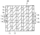
次に、本発明の第3の実施形態による半導体装置について説明する。本発明の半導体装置を適用した第3の実施形態によるパワーMOSFETは、前述した基本構造(図1に示したトレンチ・ゲート構造を有するMOSFETの基本構造)を有し、かつ図7に示す素子上部構造を有している。図7は図2と同様に、第3の実施形態によるパワーMOSFET25の素子上部構造(ソース電極20を取り除いた部分の構造)を示す平面図である。
Next, a semiconductor device according to a third embodiment of the present invention will be described. The power MOSFET according to the third embodiment to which the semiconductor device of the present invention is applied has the basic structure described above (basic structure of the MOSFET having the trench-gate structure shown in FIG. 1), and the upper portion of the element shown in FIG. It has a structure. FIG. 7 is a plan view showing the element upper structure (the structure of the portion from which the
図7に示すパワーMOSFET25の素子上部構造において、n+型ソース領域18およびp+型領域19の形成方向は、実効素子領域におけるp+型領域19の占める割合がゲート信号入力端子領域に近い領域(図中左側端部領域)より遠い領域(図中右端部領域)の方が大きくなるように、トレンチ・ゲート17の長手方向(トレンチ14の形成方向)に対して少なくとも一部が傾きを持っている。すなわち、n+型ソース領域18の基準長さL1とp+型領域19の基準長さL2との比率(L2/L1)は、ゲート信号入力端子領域に近い領域(L2A/L1A)から遠い領域(L2B/L1B)に向けて連続的に増加している。これによって、第2の実施形態と同様にオフタイミングのずれによる電流集中に対するアバランシェ耐量を高めることができる。
In the element upper structure of the
さらに、n+型ソース領域18およびp+型領域19の形成方向とトレンチ・ゲート17の長手方向とが傾きを持って配置されていることから、n+型ソース領域18とp+型領域19との界面の少なくとも一部はトレンチ・ゲート17の長手方向に対して傾いた状態で配置されている。これによって、第1の実施形態と同様にチャネル近傍で生じたブレイクダウン電流に対するn+型ソース領域18直下のもぐり抵抗が低減されることから、寄生npnバイポーラトランジスタの駆動を抑制することができる。
Further, since the formation direction of the n +
このように、第3の実施形態によるパワーMOSFET25においては、オフタイミングのずれによる電流集中に対するアバランシェ耐量の向上と寄生npnバイポーラトランジスタの駆動に基づく電流集中の緩和を共に実現することができる。これによって、パワーMOSFET25のオン抵抗の低減を図った上で、アバランシェ破壊の発生をより効果的に抑制することが可能となる。なお、パワーMOSFET25におけるL1とL2との比率や各領域18、19の形成角度等の具体的な条件は、第1および第2の実施形態と同様とすることが好ましい。
As described above, in the
10…n型ドリフト層、11…p型ベース層、12…n+型ドレイン領域、13…ドレイン電極、14…トレンチ、15…ゲート絶縁膜、16…ゲート電極材、17…トレンチ・ゲート、18…n+型ソース領域、19…p+型領域、20…ソース電極、21、22、25…パワーMOSFET、23…ゲート電極、24…ゲート信号入力端子領域。
DESCRIPTION OF
Claims (5)
前記第1の半導体層上に設けられた第2導電型の第2の半導体層と、
前記第2の半導体層を貫通して前記第1の半導体層に達するトレンチと、前記トレンチ内に絶縁膜を介して充填された導電材とを有するトレンチ・ゲートと、
前記第2の半導体層上に前記トレンチ・ゲートの前記導電材と前記絶縁膜を介して隣接形成された第1導電型の第3の半導体領域と、
前記第2の半導体層上に前記第3の半導体領域と前記トレンチ・ゲートに沿って交互に配置されるように隣接形成された第2導電型の第4の半導体領域とを具備し、
前記第3の半導体領域および前記第4の半導体領域は、前記トレンチ・ゲートの長手方向に対して傾きを持って配置されていることを特徴とする半導体装置。 A first semiconductor layer of a first conductivity type;
A second semiconductor layer of a second conductivity type provided on the first semiconductor layer;
A trench gate having a trench that penetrates the second semiconductor layer and reaches the first semiconductor layer; and a conductive material filled in the trench through an insulating film;
A third semiconductor region of a first conductivity type formed adjacent to the conductive material of the trench gate via the insulating film on the second semiconductor layer;
A second conductive type fourth semiconductor region formed adjacent to the third semiconductor region and alternately arranged along the trench gate on the second semiconductor layer;
It said third semiconductor region and said fourth semiconductor region is a semiconductor device characterized by being placed with an inclination to the longitudinal direction of the trench gate.
前記第3の半導体領域と前記第4の半導体領域との界面と前記トレンチ・ゲートの長手方向とが成す角度をαとしたとき、前記第3の半導体領域と前記第4の半導体領域は前記角度αが10〜75°の範囲となるように配置されていることを特徴とする半導体装置。When the angle formed by the interface between the third semiconductor region and the fourth semiconductor region and the longitudinal direction of the trench gate is α, the third semiconductor region and the fourth semiconductor region are at the angle. A semiconductor device, wherein α is arranged to be in a range of 10 to 75 °.
前記第1の半導体層上に設けられた第2導電型の第2の半導体層と、
前記第2の半導体層を貫通して前記第1の半導体層に達するトレンチと、前記トレンチ内に絶縁膜を介して充填された導電材とを有するトレンチ・ゲートと、
前記第2の半導体層上に前記トレンチ・ゲートの前記導電材と前記絶縁膜を介して隣接形成された第1導電型の第3の半導体領域と、
前記第2の半導体層上に前記第3の半導体領域と前記トレンチ・ゲートに沿って交互に配置されるように隣接形成された第2導電型の第4の半導体領域とを具備し、
前記第4の半導体領域は、実効素子領域における前記第4の半導体領域の占める割合が、駆動電圧が印加されるゲート信号入力端子領域に近い領域より遠い領域の方が大きくなるように形成されていることを特徴とする半導体装置。 A first semiconductor layer of a first conductivity type;
A second semiconductor layer of a second conductivity type provided on the first semiconductor layer;
A trench gate having a trench that penetrates the second semiconductor layer and reaches the first semiconductor layer; and a conductive material filled in the trench through an insulating film;
A third semiconductor region of a first conductivity type formed adjacent to the conductive material of the trench gate via the insulating film on the second semiconductor layer;
A second conductive type fourth semiconductor region formed adjacent to the third semiconductor region and alternately arranged along the trench gate on the second semiconductor layer;
The fourth semiconductor region is formed such that a ratio of the fourth semiconductor region in the effective element region is larger in a region far from a region near the gate signal input terminal region to which the driving voltage is applied. A semiconductor device characterized by comprising:
前記第1の半導体層上に設けられた第2導電型の第2の半導体層と、
前記第2の半導体層を貫通して前記第1の半導体層に達するトレンチと、前記トレンチ内に絶縁膜を介して充填された導電材とを有するトレンチ・ゲートと、
前記第2の半導体層上に前記トレンチ・ゲートの前記導電材と前記絶縁膜を介して隣接形成された第1導電型の第3の半導体領域と、
前記第2の半導体層上に前記第3の半導体領域と前記トレンチ・ゲートに沿って交互に配置されるように隣接形成された第2導電型の第4の半導体領域とを具備し、
前記第3の半導体領域および前記第4の半導体領域は少なくとも一部が前記トレンチ・ゲートの長手方向に対して傾きを持って配置されており、かつ前記第4の半導体領域は実効素子領域における前記第4の半導体領域の占める割合が、駆動電圧が印加されるゲート信号入力端子領域に近い領域より遠い領域の方が大きくなるように形成されていることを特徴とする半導体装置。 A first semiconductor layer of a first conductivity type;
A second semiconductor layer of a second conductivity type provided on the first semiconductor layer;
A trench gate having a trench that penetrates the second semiconductor layer and reaches the first semiconductor layer; and a conductive material filled in the trench through an insulating film;
A third semiconductor region of a first conductivity type formed adjacent to the conductive material of the trench gate via the insulating film on the second semiconductor layer;
A second conductive type fourth semiconductor region formed adjacent to the third semiconductor region and alternately arranged along the trench gate on the second semiconductor layer;
In the third semiconductor region and said fourth semiconductor region is placed with an inclination of at least part of the longitudinal direction of the trench gate, and said fourth semiconductor region is effective element region The semiconductor device is characterized in that a ratio of the fourth semiconductor region is larger in a region far from a region close to a gate signal input terminal region to which a driving voltage is applied.
前記第3の半導体領域が前記トレンチ・ゲートと接する部分の長さをL1、前記第4の半導体領域が前記トレンチ・ゲートと接する部分の長さをL2、これらの長さ比をL2/L1としたとき、前記第4の半導体領域は前記入力端子領域に近い領域から前記入力端子領域から遠い領域に向けて、前記長さ比L2/L1が連続的に増加するように形成されていることを特徴とする半導体装置。 The semiconductor device according to claim 3 or 4,
The length of the portion where the third semiconductor region is in contact with the trench gate is L1, the length of the portion where the fourth semiconductor region is in contact with the trench gate is L2, and the length ratio is L2 / L1. Then, the fourth semiconductor region is formed so that the length ratio L2 / L1 continuously increases from a region close to the input terminal region to a region far from the input terminal region. A featured semiconductor device.
Priority Applications (2)
| Application Number | Priority Date | Filing Date | Title |
|---|---|---|---|
| JP2004371056A JP4212552B2 (en) | 2004-12-22 | 2004-12-22 | Semiconductor device |
| US11/305,202 US7400007B2 (en) | 2004-12-22 | 2005-12-19 | Semiconductor device |
Applications Claiming Priority (1)
| Application Number | Priority Date | Filing Date | Title |
|---|---|---|---|
| JP2004371056A JP4212552B2 (en) | 2004-12-22 | 2004-12-22 | Semiconductor device |
Publications (2)
| Publication Number | Publication Date |
|---|---|
| JP2006179664A JP2006179664A (en) | 2006-07-06 |
| JP4212552B2 true JP4212552B2 (en) | 2009-01-21 |
Family
ID=36683002
Family Applications (1)
| Application Number | Title | Priority Date | Filing Date |
|---|---|---|---|
| JP2004371056A Expired - Fee Related JP4212552B2 (en) | 2004-12-22 | 2004-12-22 | Semiconductor device |
Country Status (2)
| Country | Link |
|---|---|
| US (1) | US7400007B2 (en) |
| JP (1) | JP4212552B2 (en) |
Families Citing this family (4)
| Publication number | Priority date | Publication date | Assignee | Title |
|---|---|---|---|---|
| US8084909B2 (en) * | 2009-04-09 | 2011-12-27 | Goodzeit Carl L | Dual armature motor/generator with flux linkage |
| WO2012017878A1 (en) * | 2010-08-02 | 2012-02-09 | 日産自動車株式会社 | Semiconductor device |
| CN104995737B (en) * | 2013-02-13 | 2017-10-27 | 丰田自动车株式会社 | Semiconductor device with a plurality of semiconductor chips |
| CN116110962B (en) * | 2023-04-03 | 2025-10-24 | 重庆云潼科技有限公司 | A carrier storage trench gate IGBT device with high short-circuit resistance |
Family Cites Families (5)
| Publication number | Priority date | Publication date | Assignee | Title |
|---|---|---|---|---|
| US5448083A (en) * | 1991-08-08 | 1995-09-05 | Kabushiki Kaisha Toshiba | Insulated-gate semiconductor device |
| DE69233105T2 (en) * | 1991-08-08 | 2004-05-06 | Kabushiki Kaisha Toshiba, Kawasaki | Insulated trench gate bipolar transistor |
| JP3384198B2 (en) * | 1995-07-21 | 2003-03-10 | 三菱電機株式会社 | Insulated gate semiconductor device and method of manufacturing the same |
| JP3329707B2 (en) * | 1997-09-30 | 2002-09-30 | 株式会社東芝 | Semiconductor device |
| JP4421144B2 (en) * | 2001-06-29 | 2010-02-24 | 株式会社東芝 | Semiconductor device |
-
2004
- 2004-12-22 JP JP2004371056A patent/JP4212552B2/en not_active Expired - Fee Related
-
2005
- 2005-12-19 US US11/305,202 patent/US7400007B2/en not_active Expired - Fee Related
Also Published As
| Publication number | Publication date |
|---|---|
| JP2006179664A (en) | 2006-07-06 |
| US20060157778A1 (en) | 2006-07-20 |
| US7400007B2 (en) | 2008-07-15 |
Similar Documents
| Publication | Publication Date | Title |
|---|---|---|
| JP4967236B2 (en) | Semiconductor element | |
| US9024382B2 (en) | Semiconductor device | |
| JP6323556B2 (en) | Semiconductor device | |
| WO2014163058A1 (en) | Semiconductor device | |
| JP2015213141A (en) | Vertical semiconductor device and manufacturing method thereof | |
| JP5297706B2 (en) | Semiconductor device | |
| WO2013179648A1 (en) | Semiconductor device | |
| CN104465718B (en) | Semiconductor device | |
| JP5652409B2 (en) | Semiconductor element | |
| JP6183550B2 (en) | Semiconductor device | |
| JP2008277352A (en) | Semiconductor device | |
| CN107731892A (en) | Semiconductor device | |
| JP7256771B2 (en) | semiconductor equipment | |
| JP2004241768A (en) | Semiconductor element | |
| JP2006245477A (en) | Semiconductor device | |
| JP5217158B2 (en) | Semiconductor device | |
| JP4212552B2 (en) | Semiconductor device | |
| JP2016096307A (en) | Semiconductor device | |
| JP2005150348A (en) | Semiconductor device | |
| JP2012099696A (en) | Semiconductor device | |
| JP7387501B2 (en) | Semiconductor device and its control method | |
| JP6177300B2 (en) | Semiconductor device | |
| JP6089070B2 (en) | Semiconductor device | |
| JP2009071082A (en) | Semiconductor device | |
| JP2025090230A (en) | Semiconductor Device |
Legal Events
| Date | Code | Title | Description |
|---|---|---|---|
| A977 | Report on retrieval |
Free format text: JAPANESE INTERMEDIATE CODE: A971007 Effective date: 20081009 |
|
| TRDD | Decision of grant or rejection written | ||
| A01 | Written decision to grant a patent or to grant a registration (utility model) |
Free format text: JAPANESE INTERMEDIATE CODE: A01 Effective date: 20081021 |
|
| A01 | Written decision to grant a patent or to grant a registration (utility model) |
Free format text: JAPANESE INTERMEDIATE CODE: A01 |
|
| A61 | First payment of annual fees (during grant procedure) |
Free format text: JAPANESE INTERMEDIATE CODE: A61 Effective date: 20081028 |
|
| FPAY | Renewal fee payment (event date is renewal date of database) |
Free format text: PAYMENT UNTIL: 20111107 Year of fee payment: 3 |
|
| FPAY | Renewal fee payment (event date is renewal date of database) |
Free format text: PAYMENT UNTIL: 20111107 Year of fee payment: 3 |
|
| FPAY | Renewal fee payment (event date is renewal date of database) |
Free format text: PAYMENT UNTIL: 20121107 Year of fee payment: 4 |
|
| FPAY | Renewal fee payment (event date is renewal date of database) |
Free format text: PAYMENT UNTIL: 20131107 Year of fee payment: 5 |
|
| R250 | Receipt of annual fees |
Free format text: JAPANESE INTERMEDIATE CODE: R250 |
|
| LAPS | Cancellation because of no payment of annual fees |