JP4197319B2 - シリコン窒化膜の形成方法および形成装置 - Google Patents
シリコン窒化膜の形成方法および形成装置 Download PDFInfo
- Publication number
- JP4197319B2 JP4197319B2 JP2004519275A JP2004519275A JP4197319B2 JP 4197319 B2 JP4197319 B2 JP 4197319B2 JP 2004519275 A JP2004519275 A JP 2004519275A JP 2004519275 A JP2004519275 A JP 2004519275A JP 4197319 B2 JP4197319 B2 JP 4197319B2
- Authority
- JP
- Japan
- Prior art keywords
- substrate
- gas
- silicon nitride
- nitride film
- plasma
- Prior art date
- Legal status (The legal status is an assumption and is not a legal conclusion. Google has not performed a legal analysis and makes no representation as to the accuracy of the status listed.)
- Expired - Fee Related
Links
Images
Classifications
-
- H—ELECTRICITY
- H10—SEMICONDUCTOR DEVICES; ELECTRIC SOLID-STATE DEVICES NOT OTHERWISE PROVIDED FOR
- H10P—GENERIC PROCESSES OR APPARATUS FOR THE MANUFACTURE OR TREATMENT OF DEVICES COVERED BY CLASS H10
- H10P14/00—Formation of materials, e.g. in the shape of layers or pillars
- H10P14/60—Formation of materials, e.g. in the shape of layers or pillars of insulating materials
- H10P14/69—Inorganic materials
- H10P14/694—Inorganic materials composed of nitrides
- H10P14/6943—Inorganic materials composed of nitrides containing silicon
- H10P14/69433—Inorganic materials composed of nitrides containing silicon the material being a silicon nitride not containing oxygen, e.g. SixNy or SixByNz
-
- C—CHEMISTRY; METALLURGY
- C23—COATING METALLIC MATERIAL; COATING MATERIAL WITH METALLIC MATERIAL; CHEMICAL SURFACE TREATMENT; DIFFUSION TREATMENT OF METALLIC MATERIAL; COATING BY VACUUM EVAPORATION, BY SPUTTERING, BY ION IMPLANTATION OR BY CHEMICAL VAPOUR DEPOSITION, IN GENERAL; INHIBITING CORROSION OF METALLIC MATERIAL OR INCRUSTATION IN GENERAL
- C23C—COATING METALLIC MATERIAL; COATING MATERIAL WITH METALLIC MATERIAL; SURFACE TREATMENT OF METALLIC MATERIAL BY DIFFUSION INTO THE SURFACE, BY CHEMICAL CONVERSION OR SUBSTITUTION; COATING BY VACUUM EVAPORATION, BY SPUTTERING, BY ION IMPLANTATION OR BY CHEMICAL VAPOUR DEPOSITION, IN GENERAL
- C23C16/00—Chemical coating by decomposition of gaseous compounds, without leaving reaction products of surface material in the coating, i.e. chemical vapour deposition [CVD] processes
- C23C16/22—Chemical coating by decomposition of gaseous compounds, without leaving reaction products of surface material in the coating, i.e. chemical vapour deposition [CVD] processes characterised by the deposition of inorganic material, other than metallic material
- C23C16/30—Deposition of compounds, mixtures or solid solutions, e.g. borides, carbides, nitrides
- C23C16/34—Nitrides
- C23C16/345—Silicon nitride
-
- C—CHEMISTRY; METALLURGY
- C23—COATING METALLIC MATERIAL; COATING MATERIAL WITH METALLIC MATERIAL; CHEMICAL SURFACE TREATMENT; DIFFUSION TREATMENT OF METALLIC MATERIAL; COATING BY VACUUM EVAPORATION, BY SPUTTERING, BY ION IMPLANTATION OR BY CHEMICAL VAPOUR DEPOSITION, IN GENERAL; INHIBITING CORROSION OF METALLIC MATERIAL OR INCRUSTATION IN GENERAL
- C23C—COATING METALLIC MATERIAL; COATING MATERIAL WITH METALLIC MATERIAL; SURFACE TREATMENT OF METALLIC MATERIAL BY DIFFUSION INTO THE SURFACE, BY CHEMICAL CONVERSION OR SUBSTITUTION; COATING BY VACUUM EVAPORATION, BY SPUTTERING, BY ION IMPLANTATION OR BY CHEMICAL VAPOUR DEPOSITION, IN GENERAL
- C23C16/00—Chemical coating by decomposition of gaseous compounds, without leaving reaction products of surface material in the coating, i.e. chemical vapour deposition [CVD] processes
- C23C16/44—Chemical coating by decomposition of gaseous compounds, without leaving reaction products of surface material in the coating, i.e. chemical vapour deposition [CVD] processes characterised by the method of coating
- C23C16/448—Chemical coating by decomposition of gaseous compounds, without leaving reaction products of surface material in the coating, i.e. chemical vapour deposition [CVD] processes characterised by the method of coating characterised by the method used for generating reactive gas streams, e.g. by evaporation or sublimation of precursor materials
- C23C16/452—Chemical coating by decomposition of gaseous compounds, without leaving reaction products of surface material in the coating, i.e. chemical vapour deposition [CVD] processes characterised by the method of coating characterised by the method used for generating reactive gas streams, e.g. by evaporation or sublimation of precursor materials by activating reactive gas streams before their introduction into the reaction chamber, e.g. by ionisation or addition of reactive species
-
- H—ELECTRICITY
- H10—SEMICONDUCTOR DEVICES; ELECTRIC SOLID-STATE DEVICES NOT OTHERWISE PROVIDED FOR
- H10P—GENERIC PROCESSES OR APPARATUS FOR THE MANUFACTURE OR TREATMENT OF DEVICES COVERED BY CLASS H10
- H10P14/00—Formation of materials, e.g. in the shape of layers or pillars
- H10P14/60—Formation of materials, e.g. in the shape of layers or pillars of insulating materials
- H10P14/66—Formation of materials, e.g. in the shape of layers or pillars of insulating materials characterised by the type of materials
- H10P14/668—Formation of materials, e.g. in the shape of layers or pillars of insulating materials characterised by the type of materials the materials being characterised by the deposition precursor materials
- H10P14/6681—Formation of materials, e.g. in the shape of layers or pillars of insulating materials characterised by the type of materials the materials being characterised by the deposition precursor materials the precursor containing a compound comprising Si
- H10P14/6687—Formation of materials, e.g. in the shape of layers or pillars of insulating materials characterised by the type of materials the materials being characterised by the deposition precursor materials the precursor containing a compound comprising Si the compound comprising silicon and nitrogen
- H10P14/6689—Formation of materials, e.g. in the shape of layers or pillars of insulating materials characterised by the type of materials the materials being characterised by the deposition precursor materials the precursor containing a compound comprising Si the compound comprising silicon and nitrogen the compound being a silazane
-
- H—ELECTRICITY
- H10—SEMICONDUCTOR DEVICES; ELECTRIC SOLID-STATE DEVICES NOT OTHERWISE PROVIDED FOR
- H10P—GENERIC PROCESSES OR APPARATUS FOR THE MANUFACTURE OR TREATMENT OF DEVICES COVERED BY CLASS H10
- H10P95/00—Generic processes or apparatus for manufacture or treatments not covered by the other groups of this subclass
- H10P95/90—Thermal treatments, e.g. annealing or sintering
-
- H—ELECTRICITY
- H10—SEMICONDUCTOR DEVICES; ELECTRIC SOLID-STATE DEVICES NOT OTHERWISE PROVIDED FOR
- H10P—GENERIC PROCESSES OR APPARATUS FOR THE MANUFACTURE OR TREATMENT OF DEVICES COVERED BY CLASS H10
- H10P14/00—Formation of materials, e.g. in the shape of layers or pillars
- H10P14/60—Formation of materials, e.g. in the shape of layers or pillars of insulating materials
- H10P14/63—Formation of materials, e.g. in the shape of layers or pillars of insulating materials characterised by the formation processes
- H10P14/6326—Deposition processes
- H10P14/6328—Deposition from the gas or vapour phase
- H10P14/6334—Deposition from the gas or vapour phase using decomposition or reaction of gaseous or vapour phase compounds, i.e. chemical vapour deposition
- H10P14/6336—Deposition from the gas or vapour phase using decomposition or reaction of gaseous or vapour phase compounds, i.e. chemical vapour deposition in the presence of a plasma [PECVD]
Landscapes
- Chemical & Material Sciences (AREA)
- General Chemical & Material Sciences (AREA)
- Chemical Kinetics & Catalysis (AREA)
- Engineering & Computer Science (AREA)
- Materials Engineering (AREA)
- Mechanical Engineering (AREA)
- Metallurgy (AREA)
- Organic Chemistry (AREA)
- Inorganic Chemistry (AREA)
- Chemical Vapour Deposition (AREA)
- Formation Of Insulating Films (AREA)
Description
前記基板の収容される前記処理容器内に、前記処理容器の底板に固設される噴射ノズルから上方の前記基板に向かって、ヘキサメチルジシラザン{(CH3)3SiNHSi(CH3)3}とプラズマ励起されたN 2 またはNH 3 のうち少なくともいずれか1種の窒素化合物からなるガスとを、基板付近における反応生成物が生成される領域の圧力よりも前記窒素化合物がプラズマ励起される領域の圧力の方が高くなるようにして供給し、
前記ヘキサメチルジシラザンガスと前記プラズマ励起された窒素化合物からなるガスとの反応生成物を前記基板上に堆積させてシリコン窒化膜を形成することを特徴とするシリコン窒化膜の形成方法である。
本発明に従えば、基板が室温〜800℃に加熱されるので、基板付近における窒素化合物がプラズマ励起されて形成される活性種とヘキサアルキルジシラザンとのエネルギ授受および反応生成物の生成が促進され、基板上へのシリコン窒化膜の堆積が一層効率よく行われる。
前記基板を内部空間に収容する処理容器と、
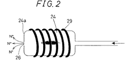
噴射孔が基板を臨み、噴射孔から上方に向かって噴射されるヘキサアルキルジシラザンガスが基板付近に供給されるように、前記処理容器の底板に固設される第1噴射ノズルを有し、前記処理容器の内部空間にヘキサアルキルジシラザンガスを供給する第1ガス供給手段と、
噴射孔が基板を臨み、噴射孔から上方に向かって噴射される窒素化合物からなるガスが基板付近に供給されるように、前記処理容器の底板に固設される第2噴射ノズルを有し、前記処理容器の内部空間に窒素化合物からなるガスを供給する第2ガス供給手段と、
前記第2ガス供給手段に設けられ、前記処理容器の内部空間に供給される窒素化合物からなるガスをプラズマ励起するプラズマ励起手段と、
前記基板を加熱する加熱手段とを含み、
前記処理容器の内部空間にガスを供給する前記第2ガス供給手段のガス供給部は、オリフィス構造を有し、
前記ヘキサアルキルジシラザンは、ヘキサメチルジシラザンであり、
前記窒素化合物は、N2またはNH3のうち少なくともいずれか1種であることを特徴とするシリコン窒化膜の形成装置である。
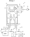
図1は、本発明の実施の一形態であるシリコン窒化膜の形成装置1の構成を簡略化して示す図である。シリコン窒化膜の形成装置1は、基板2を内部空間3に収容する処理容器4と、処理容器4の内部空間3にHMDSガスを供給する第1ガス供給手段5と、処理容器4の内部空間3にN2ガスを供給する第2ガス供給手段6と、第2ガス供給手段6に設けられ処理容器4の内部空間3に供給されるN2ガスをプラズマ励起するプラズマ励起手段7と、基板2を加熱する加熱手段8とを含む。
以下に本発明の実施例を説明する。
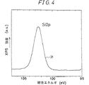
シリコン窒化膜の形成装置1を準備し、シリコン窒化膜のSi源にHMDSを用い、N源にN2ガスを用いて、シリコンウェハの基板上にシリコン窒化膜を形成した。シリコン窒化膜形成に用いた条件をまとめて表1に示す。なお、形成装置1に備わる処理容器4の内部空間3の容積は大略1000L(リットル)であった。
2 基板
3 内部空間
4 処理容器
5 第1ガス供給手段
6 第2ガス供給手段
7 プラズマ励起手段
8 加熱手段
12 真空ポンプ
13 シャッタ
Claims (4)
- 基板を処理容器の内部空間に収容し、
前記基板の収容される前記処理容器内に、前記処理容器の底板に固設される噴射ノズルから上方の前記基板に向かって、ヘキサメチルジシラザン{(CH3)3SiNHSi(CH3)3}ガスとプラズマ励起されたN 2 またはNH 3 のうち少なくともいずれか1種の窒素化合物からなるガスとを、基板付近における反応生成物が生成される領域の圧力よりも前記窒素化合物がプラズマ励起される領域の圧力の方が高くなるようにして供給し、
前記ヘキサメチルジシラザンガスと前記プラズマ励起された窒素化合物からなるガスとの反応生成物を前記基板上に堆積させてシリコン窒化膜を形成することを特徴とするシリコン窒化膜の形成方法。 - 基板を処理容器の内部空間に収容し、
前記基板の収容される前記処理容器内に、前記処理容器の底板に固設される噴射ノズルから上方の前記基板に向かって、第一噴射ノズルでヘキサメチルジシラザン{(CH3)3SiNHSi(CH3)3}ガスを供給し、オリフィス構造を有する第二噴射ノズルでプラズマ励起されたN 2 またはNH 3 のうち少なくともいずれか1種の窒素化合物からなるガスを供給し、
前記ヘキサメチルジシラザンガスと前記プラズマ励起された窒素化合物からなるガスとの反応生成物を前記基板上に堆積させてシリコン窒化膜を形成することを特徴とするシリコン窒化膜の形成方法。 - 前記基板は、室温〜800℃に加熱されることを特徴とする請求項1〜2記載のシリコン窒化膜の形成方法。
- 基板の表面にシリコン窒化膜を形成するシリコン窒化膜の形成装置であって、
前記基板を内部空間に収容する処理容器と、
噴射孔が基板を臨み、噴射孔から上方に向かって噴射されるヘキサアルキルジシラザンガスが基板付近に供給されるように、前記処理容器の底板に固設される第1噴射ノズルを有し、前記処理容器の内部空間にヘキサアルキルジシラザンガスを供給する第1ガス供給手段と、
噴射孔が基板を臨み、噴射孔から上方に向かって噴射される窒素化合物からなるガスが基板付近に供給されるように、前記処理容器の底板に固設される第2噴射ノズルを有し、前記処理容器の内部空間に窒素化合物からなるガスを供給する第2ガス供給手段と、
前記第2ガス供給手段に設けられ、前記処理容器の内部空間に供給される窒素化合物からなるガスをプラズマ励起するプラズマ励起手段と、
前記基板を加熱する加熱手段とを含み、
前記処理容器の内部空間にガスを供給する前記第2ガス供給手段のガス供給部は、オリフィス構造を有し、
前記ヘキサアルキルジシラザンは、ヘキサメチルジシラザンであり、
前記窒素化合物は、N2またはNH3のうち少なくともいずれか1種であることを特徴とするシリコン窒化膜の形成装置。
Applications Claiming Priority (3)
| Application Number | Priority Date | Filing Date | Title |
|---|---|---|---|
| JP2002199122 | 2002-07-08 | ||
| JP2002199122 | 2002-07-08 | ||
| PCT/JP2003/008552 WO2004006321A1 (ja) | 2002-07-08 | 2003-07-04 | シリコン窒化膜の形成方法および形成装置 |
Publications (2)
| Publication Number | Publication Date |
|---|---|
| JPWO2004006321A1 JPWO2004006321A1 (ja) | 2005-11-10 |
| JP4197319B2 true JP4197319B2 (ja) | 2008-12-17 |
Family
ID=30112450
Family Applications (1)
| Application Number | Title | Priority Date | Filing Date |
|---|---|---|---|
| JP2004519275A Expired - Fee Related JP4197319B2 (ja) | 2002-07-08 | 2003-07-04 | シリコン窒化膜の形成方法および形成装置 |
Country Status (5)
| Country | Link |
|---|---|
| US (1) | US20050255713A1 (ja) |
| JP (1) | JP4197319B2 (ja) |
| KR (1) | KR100623562B1 (ja) |
| AU (1) | AU2003281403A1 (ja) |
| WO (1) | WO2004006321A1 (ja) |
Families Citing this family (13)
| Publication number | Priority date | Publication date | Assignee | Title |
|---|---|---|---|---|
| DE10350752A1 (de) * | 2003-10-30 | 2005-06-09 | Infineon Technologies Ag | Verfahren zum Ausbilden eines Dielektrikums auf einer kupferhaltigen Metallisierung und Kondensatoranordnung |
| US20050214456A1 (en) * | 2004-03-29 | 2005-09-29 | Donghul Lu | Enhanced dielectric layers using sequential deposition |
| US20060192183A1 (en) * | 2005-02-28 | 2006-08-31 | Andreas Klyszcz | Metal ink, method of preparing the metal ink, substrate for display, and method of manufacturing the substrate |
| JP4228150B2 (ja) * | 2005-03-23 | 2009-02-25 | 東京エレクトロン株式会社 | 成膜装置、成膜方法及び記憶媒体 |
| DE102006035563A1 (de) * | 2006-07-27 | 2008-01-31 | Kimes, Karin | Silan freie plasmagestützte CVD-Abscheidung von Siliziumnitrid als anti-reflektierendem Film und zur Wasserstoffpassivierung von auf Siliziumwafern aufgebauten Photozellen |
| US7638170B2 (en) * | 2007-06-21 | 2009-12-29 | Asm International N.V. | Low resistivity metal carbonitride thin film deposition by atomic layer deposition |
| US8017182B2 (en) * | 2007-06-21 | 2011-09-13 | Asm International N.V. | Method for depositing thin films by mixed pulsed CVD and ALD |
| US7867923B2 (en) * | 2007-10-22 | 2011-01-11 | Applied Materials, Inc. | High quality silicon oxide films by remote plasma CVD from disilane precursors |
| JP5883049B2 (ja) * | 2014-03-04 | 2016-03-09 | 株式会社日立国際電気 | 半導体装置の製造方法、基板処理装置、プログラムおよび記録媒体 |
| KR101909110B1 (ko) * | 2016-08-18 | 2018-10-18 | 피에스케이 주식회사 | 기판 처리 방법 |
| JP6777614B2 (ja) * | 2017-09-26 | 2020-10-28 | 株式会社Kokusai Electric | 半導体装置の製造方法、基板処理装置、およびプログラム |
| US20190386256A1 (en) * | 2018-06-18 | 2019-12-19 | Universal Display Corporation | Sequential material sources for thermally challenged OLED materials |
| JP7779632B2 (ja) * | 2022-04-18 | 2025-12-03 | 東京エレクトロン株式会社 | 成膜方法 |
Family Cites Families (11)
| Publication number | Priority date | Publication date | Assignee | Title |
|---|---|---|---|---|
| JPS54123599A (en) * | 1978-03-17 | 1979-09-25 | Toshiba Corp | Forming method for silicon nitride film |
| JPS6333575A (ja) * | 1986-07-28 | 1988-02-13 | Nippon Soken Inc | 電子サイクロトロンプラズマcvd装置 |
| KR920002864B1 (ko) * | 1987-07-20 | 1992-04-06 | 가부시기가이샤 히다찌세이사꾸쇼 | 플라즈마 처리방법 및 그 장치 |
| JPH01298164A (ja) * | 1988-05-25 | 1989-12-01 | Canon Inc | 機能性堆積膜の形成方法 |
| JP2861600B2 (ja) * | 1992-03-04 | 1999-02-24 | 日本電気株式会社 | シリコンエピタキシャル膜の選択成長方法及び成長装置 |
| JPH05263255A (ja) * | 1992-03-19 | 1993-10-12 | Hitachi Electron Eng Co Ltd | プラズマcvd装置 |
| JPH07335395A (ja) * | 1994-04-13 | 1995-12-22 | Rikagaku Kenkyusho | プラズマ発生方法およびそれを用いた成膜方法、エッチング方法、半導体堆積方法ならびにドーピング方法 |
| JPH07288237A (ja) * | 1994-04-15 | 1995-10-31 | Nippon Steel Corp | プラズマ励起セル装置 |
| JPH08321504A (ja) * | 1995-05-24 | 1996-12-03 | Ulvac Japan Ltd | 窒化物用mocvd装置 |
| JPH0941147A (ja) * | 1995-07-31 | 1997-02-10 | Canon Inc | プラズマcvd方法 |
| JPH11265883A (ja) * | 1998-03-17 | 1999-09-28 | Asahi Kasei Micro Syst Co Ltd | 半導体製造装置及び反応室用プロセスチューブ |
-
2003
- 2003-07-04 US US10/520,815 patent/US20050255713A1/en not_active Abandoned
- 2003-07-04 JP JP2004519275A patent/JP4197319B2/ja not_active Expired - Fee Related
- 2003-07-04 WO PCT/JP2003/008552 patent/WO2004006321A1/ja not_active Ceased
- 2003-07-04 KR KR1020057000364A patent/KR100623562B1/ko not_active Expired - Fee Related
- 2003-07-04 AU AU2003281403A patent/AU2003281403A1/en not_active Abandoned
Also Published As
| Publication number | Publication date |
|---|---|
| KR100623562B1 (ko) | 2006-09-13 |
| AU2003281403A1 (en) | 2004-01-23 |
| WO2004006321A1 (ja) | 2004-01-15 |
| JPWO2004006321A1 (ja) | 2005-11-10 |
| KR20050021446A (ko) | 2005-03-07 |
| US20050255713A1 (en) | 2005-11-17 |
Similar Documents
| Publication | Publication Date | Title |
|---|---|---|
| US10361088B2 (en) | Techniques and systems for continuous-flow plasma enhanced atomic layer deposition (PEALD) | |
| JP4197319B2 (ja) | シリコン窒化膜の形成方法および形成装置 | |
| US10804098B2 (en) | Systems and methods for thin-film deposition of metal oxides using excited nitrogen-oxygen species | |
| US7531467B2 (en) | Manufacturing method of semiconductor device and substrate processing apparatus | |
| KR100988096B1 (ko) | 실리콘 함유 필름의 플라즈마 시클릭 화학 증기 증착법 | |
| US8877655B2 (en) | Systems and methods for thin-film deposition of metal oxides using excited nitrogen-oxygen species | |
| CN101048853B (zh) | 用于膜形成的前驱体和用于形成含钌膜的方法 | |
| KR101293041B1 (ko) | 반도체 장치의 제조 방법, 기판 처리 방법, 기판 처리 장치 및 기록 매체 | |
| KR101726946B1 (ko) | 반도체 장치의 제조 방법, 기판 처리 장치 및 프로그램 | |
| US20050223982A1 (en) | Apparatus and method for depositing thin film on wafer using remote plasma | |
| US20050070126A1 (en) | System and method for forming multi-component dielectric films | |
| US20110070380A1 (en) | Systems and methods for thin-film deposition of metal oxides using excited nitrogen-oxygen species | |
| JP3700177B2 (ja) | 大気圧プラズマ表面処理装置 | |
| CN110402477A (zh) | 在氧化硅存在下硅表面上氧化硅或氮化硅的选择性生长 | |
| JP2005079141A (ja) | プラズマcvd装置 | |
| US11087959B2 (en) | Techniques for a hybrid design for efficient and economical plasma enhanced atomic layer deposition (PEALD) and plasma enhanced chemical vapor deposition (PECVD) | |
| WO2004066377A1 (ja) | 被処理基板上にシリコン窒化膜を形成するcvd方法 | |
| CN101014730A (zh) | 用于形成多组分介电膜的系统和方法 | |
| US20170011908A1 (en) | Method of manufacturing semiconductor device, substrate processing apparatus, and recording medium | |
| KR20110118564A (ko) | 기판 처리 장치 및 반도체 장치의 제조 방법 | |
| KR20160031413A (ko) | 반도체 장치의 제조 방법, 기판 처리 장치 및 프로그램 | |
| CN112458435B (zh) | 原子层沉积设备及清洗方法 | |
| JP4624991B2 (ja) | 酸窒化膜の形成方法、及び形成装置 | |
| TW306937B (ja) | ||
| JPH05263255A (ja) | プラズマcvd装置 |
Legal Events
| Date | Code | Title | Description |
|---|---|---|---|
| A131 | Notification of reasons for refusal |
Free format text: JAPANESE INTERMEDIATE CODE: A131 Effective date: 20070710 |
|
| A521 | Request for written amendment filed |
Free format text: JAPANESE INTERMEDIATE CODE: A523 Effective date: 20070910 |
|
| A711 | Notification of change in applicant |
Free format text: JAPANESE INTERMEDIATE CODE: A711 Effective date: 20070910 |
|
| A521 | Request for written amendment filed |
Free format text: JAPANESE INTERMEDIATE CODE: A523 Effective date: 20070918 |
|
| A131 | Notification of reasons for refusal |
Free format text: JAPANESE INTERMEDIATE CODE: A131 Effective date: 20071211 |
|
| A02 | Decision of refusal |
Free format text: JAPANESE INTERMEDIATE CODE: A02 Effective date: 20080311 |
|
| A521 | Request for written amendment filed |
Free format text: JAPANESE INTERMEDIATE CODE: A523 Effective date: 20080512 |
|
| A521 | Request for written amendment filed |
Free format text: JAPANESE INTERMEDIATE CODE: A821 Effective date: 20080512 |
|
| RD02 | Notification of acceptance of power of attorney |
Free format text: JAPANESE INTERMEDIATE CODE: A7422 Effective date: 20080626 |
|
| A521 | Request for written amendment filed |
Free format text: JAPANESE INTERMEDIATE CODE: A821 Effective date: 20080701 |
|
| RD04 | Notification of resignation of power of attorney |
Free format text: JAPANESE INTERMEDIATE CODE: A7424 Effective date: 20080701 |
|
| A521 | Request for written amendment filed |
Free format text: JAPANESE INTERMEDIATE CODE: A523 Effective date: 20080717 |
|
| A911 | Transfer to examiner for re-examination before appeal (zenchi) |
Free format text: JAPANESE INTERMEDIATE CODE: A911 Effective date: 20080723 |
|
| TRDD | Decision of grant or rejection written | ||
| A01 | Written decision to grant a patent or to grant a registration (utility model) |
Free format text: JAPANESE INTERMEDIATE CODE: A01 Effective date: 20080924 |
|
| A01 | Written decision to grant a patent or to grant a registration (utility model) |
Free format text: JAPANESE INTERMEDIATE CODE: A01 |
|
| A61 | First payment of annual fees (during grant procedure) |
Free format text: JAPANESE INTERMEDIATE CODE: A61 Effective date: 20080925 |
|
| FPAY | Renewal fee payment (event date is renewal date of database) |
Free format text: PAYMENT UNTIL: 20111010 Year of fee payment: 3 |
|
| R150 | Certificate of patent or registration of utility model |
Free format text: JAPANESE INTERMEDIATE CODE: R150 |
|
| FPAY | Renewal fee payment (event date is renewal date of database) |
Free format text: PAYMENT UNTIL: 20111010 Year of fee payment: 3 |
|
| FPAY | Renewal fee payment (event date is renewal date of database) |
Free format text: PAYMENT UNTIL: 20131010 Year of fee payment: 5 |
|
| LAPS | Cancellation because of no payment of annual fees |