JP4197319B2 - Method and apparatus for forming silicon nitride film - Google Patents
Method and apparatus for forming silicon nitride film Download PDFInfo
- Publication number
- JP4197319B2 JP4197319B2 JP2004519275A JP2004519275A JP4197319B2 JP 4197319 B2 JP4197319 B2 JP 4197319B2 JP 2004519275 A JP2004519275 A JP 2004519275A JP 2004519275 A JP2004519275 A JP 2004519275A JP 4197319 B2 JP4197319 B2 JP 4197319B2
- Authority
- JP
- Japan
- Prior art keywords
- substrate
- gas
- silicon nitride
- nitride film
- plasma
- Prior art date
- Legal status (The legal status is an assumption and is not a legal conclusion. Google has not performed a legal analysis and makes no representation as to the accuracy of the status listed.)
- Expired - Fee Related
Links
Images
Classifications
-
- H—ELECTRICITY
- H10—SEMICONDUCTOR DEVICES; ELECTRIC SOLID-STATE DEVICES NOT OTHERWISE PROVIDED FOR
- H10P—GENERIC PROCESSES OR APPARATUS FOR THE MANUFACTURE OR TREATMENT OF DEVICES COVERED BY CLASS H10
- H10P14/00—Formation of materials, e.g. in the shape of layers or pillars
- H10P14/60—Formation of materials, e.g. in the shape of layers or pillars of insulating materials
- H10P14/69—Inorganic materials
- H10P14/694—Inorganic materials composed of nitrides
- H10P14/6943—Inorganic materials composed of nitrides containing silicon
- H10P14/69433—Inorganic materials composed of nitrides containing silicon the material being a silicon nitride not containing oxygen, e.g. SixNy or SixByNz
-
- C—CHEMISTRY; METALLURGY
- C23—COATING METALLIC MATERIAL; COATING MATERIAL WITH METALLIC MATERIAL; CHEMICAL SURFACE TREATMENT; DIFFUSION TREATMENT OF METALLIC MATERIAL; COATING BY VACUUM EVAPORATION, BY SPUTTERING, BY ION IMPLANTATION OR BY CHEMICAL VAPOUR DEPOSITION, IN GENERAL; INHIBITING CORROSION OF METALLIC MATERIAL OR INCRUSTATION IN GENERAL
- C23C—COATING METALLIC MATERIAL; COATING MATERIAL WITH METALLIC MATERIAL; SURFACE TREATMENT OF METALLIC MATERIAL BY DIFFUSION INTO THE SURFACE, BY CHEMICAL CONVERSION OR SUBSTITUTION; COATING BY VACUUM EVAPORATION, BY SPUTTERING, BY ION IMPLANTATION OR BY CHEMICAL VAPOUR DEPOSITION, IN GENERAL
- C23C16/00—Chemical coating by decomposition of gaseous compounds, without leaving reaction products of surface material in the coating, i.e. chemical vapour deposition [CVD] processes
- C23C16/22—Chemical coating by decomposition of gaseous compounds, without leaving reaction products of surface material in the coating, i.e. chemical vapour deposition [CVD] processes characterised by the deposition of inorganic material, other than metallic material
- C23C16/30—Deposition of compounds, mixtures or solid solutions, e.g. borides, carbides, nitrides
- C23C16/34—Nitrides
- C23C16/345—Silicon nitride
-
- C—CHEMISTRY; METALLURGY
- C23—COATING METALLIC MATERIAL; COATING MATERIAL WITH METALLIC MATERIAL; CHEMICAL SURFACE TREATMENT; DIFFUSION TREATMENT OF METALLIC MATERIAL; COATING BY VACUUM EVAPORATION, BY SPUTTERING, BY ION IMPLANTATION OR BY CHEMICAL VAPOUR DEPOSITION, IN GENERAL; INHIBITING CORROSION OF METALLIC MATERIAL OR INCRUSTATION IN GENERAL
- C23C—COATING METALLIC MATERIAL; COATING MATERIAL WITH METALLIC MATERIAL; SURFACE TREATMENT OF METALLIC MATERIAL BY DIFFUSION INTO THE SURFACE, BY CHEMICAL CONVERSION OR SUBSTITUTION; COATING BY VACUUM EVAPORATION, BY SPUTTERING, BY ION IMPLANTATION OR BY CHEMICAL VAPOUR DEPOSITION, IN GENERAL
- C23C16/00—Chemical coating by decomposition of gaseous compounds, without leaving reaction products of surface material in the coating, i.e. chemical vapour deposition [CVD] processes
- C23C16/44—Chemical coating by decomposition of gaseous compounds, without leaving reaction products of surface material in the coating, i.e. chemical vapour deposition [CVD] processes characterised by the method of coating
- C23C16/448—Chemical coating by decomposition of gaseous compounds, without leaving reaction products of surface material in the coating, i.e. chemical vapour deposition [CVD] processes characterised by the method of coating characterised by the method used for generating reactive gas streams, e.g. by evaporation or sublimation of precursor materials
- C23C16/452—Chemical coating by decomposition of gaseous compounds, without leaving reaction products of surface material in the coating, i.e. chemical vapour deposition [CVD] processes characterised by the method of coating characterised by the method used for generating reactive gas streams, e.g. by evaporation or sublimation of precursor materials by activating reactive gas streams before their introduction into the reaction chamber, e.g. by ionisation or addition of reactive species
-
- H—ELECTRICITY
- H10—SEMICONDUCTOR DEVICES; ELECTRIC SOLID-STATE DEVICES NOT OTHERWISE PROVIDED FOR
- H10P—GENERIC PROCESSES OR APPARATUS FOR THE MANUFACTURE OR TREATMENT OF DEVICES COVERED BY CLASS H10
- H10P14/00—Formation of materials, e.g. in the shape of layers or pillars
- H10P14/60—Formation of materials, e.g. in the shape of layers or pillars of insulating materials
- H10P14/66—Formation of materials, e.g. in the shape of layers or pillars of insulating materials characterised by the type of materials
- H10P14/668—Formation of materials, e.g. in the shape of layers or pillars of insulating materials characterised by the type of materials the materials being characterised by the deposition precursor materials
- H10P14/6681—Formation of materials, e.g. in the shape of layers or pillars of insulating materials characterised by the type of materials the materials being characterised by the deposition precursor materials the precursor containing a compound comprising Si
- H10P14/6687—Formation of materials, e.g. in the shape of layers or pillars of insulating materials characterised by the type of materials the materials being characterised by the deposition precursor materials the precursor containing a compound comprising Si the compound comprising silicon and nitrogen
- H10P14/6689—Formation of materials, e.g. in the shape of layers or pillars of insulating materials characterised by the type of materials the materials being characterised by the deposition precursor materials the precursor containing a compound comprising Si the compound comprising silicon and nitrogen the compound being a silazane
-
- H—ELECTRICITY
- H10—SEMICONDUCTOR DEVICES; ELECTRIC SOLID-STATE DEVICES NOT OTHERWISE PROVIDED FOR
- H10P—GENERIC PROCESSES OR APPARATUS FOR THE MANUFACTURE OR TREATMENT OF DEVICES COVERED BY CLASS H10
- H10P95/00—Generic processes or apparatus for manufacture or treatments not covered by the other groups of this subclass
- H10P95/90—Thermal treatments, e.g. annealing or sintering
-
- H—ELECTRICITY
- H10—SEMICONDUCTOR DEVICES; ELECTRIC SOLID-STATE DEVICES NOT OTHERWISE PROVIDED FOR
- H10P—GENERIC PROCESSES OR APPARATUS FOR THE MANUFACTURE OR TREATMENT OF DEVICES COVERED BY CLASS H10
- H10P14/00—Formation of materials, e.g. in the shape of layers or pillars
- H10P14/60—Formation of materials, e.g. in the shape of layers or pillars of insulating materials
- H10P14/63—Formation of materials, e.g. in the shape of layers or pillars of insulating materials characterised by the formation processes
- H10P14/6326—Deposition processes
- H10P14/6328—Deposition from the gas or vapour phase
- H10P14/6334—Deposition from the gas or vapour phase using decomposition or reaction of gaseous or vapour phase compounds, i.e. chemical vapour deposition
- H10P14/6336—Deposition from the gas or vapour phase using decomposition or reaction of gaseous or vapour phase compounds, i.e. chemical vapour deposition in the presence of a plasma [PECVD]
Landscapes
- Chemical & Material Sciences (AREA)
- General Chemical & Material Sciences (AREA)
- Chemical Kinetics & Catalysis (AREA)
- Engineering & Computer Science (AREA)
- Materials Engineering (AREA)
- Mechanical Engineering (AREA)
- Metallurgy (AREA)
- Organic Chemistry (AREA)
- Inorganic Chemistry (AREA)
- Chemical Vapour Deposition (AREA)
- Formation Of Insulating Films (AREA)
Description
本発明は、たとえば集積回路基板の表面などに絶縁膜や保護膜として施されるシリコン窒化膜の形成方法および形成装置に関する。 The present invention relates to a method and an apparatus for forming a silicon nitride film applied as an insulating film or a protective film on the surface of an integrated circuit substrate, for example.
集積回路基板には、多くの電極が形成されるので電極間を絶縁するための絶縁膜、また大気中の水分などから回路を保護するための保護膜いわゆるパッシベーション膜が形成される。たとえば半導体集積回路基板の1種であるMOSFET(Metal-Oxide-Semiconductor Field Effect Transistor)などでは、従来、シリコンウェハを熱酸化することによって形成されるシリコン酸化膜(SiO2)がゲート絶縁膜に用いられている。しかしながら、シリコン酸化膜は、緻密性に劣るので、異種材料を積層したとき、異種材料の構成元素が不純物としてシリコン酸化膜中を拡散し易く、不純物がシリコン酸化膜中を拡散して基板または電極に達することによって、半導体性能が阻害されるという問題がある。またシリコン酸化膜は、比誘電率が4.0程度であるので、たとえばMOSFETのゲート絶縁膜として使用されると、ゲート容量が小さくなるという問題がある。 Since many electrodes are formed on the integrated circuit substrate, an insulating film for insulating the electrodes and a protective film for protecting the circuit from moisture in the atmosphere, a so-called passivation film is formed. For example, in a MOSFET (Metal-Oxide-Semiconductor Field Effect Transistor) which is a kind of semiconductor integrated circuit substrate, a silicon oxide film (SiO 2 ) formed by thermally oxidizing a silicon wafer is conventionally used as a gate insulating film. It has been. However, since the silicon oxide film is inferior in density, when different materials are stacked, the constituent elements of the different materials are easily diffused in the silicon oxide film as impurities, and the impurities diffuse in the silicon oxide film to cause the substrate or electrode. As a result, the semiconductor performance is hindered. Further, since the relative dielectric constant of the silicon oxide film is about 4.0, there is a problem that the gate capacitance is reduced when used as a gate insulating film of a MOSFET, for example.
このような問題点を解決する技術の一つに、シリコン酸化膜に代えてシリコン窒化膜を用いる方法がある。シリコン窒化膜は、シリコン酸化膜に比較して緻密性に優れるとともに比誘電率も7.5程度と高く、さらに耐湿性にも優れるので、前述のシリコン酸化膜に代わる絶縁膜として適するばかりでなく、パッシベーション膜としても適している。 One technique for solving such problems is to use a silicon nitride film instead of the silicon oxide film. The silicon nitride film is not only suitable as an insulating film to replace the silicon oxide film described above, because it is excellent in denseness as compared with the silicon oxide film, has a high relative dielectric constant of about 7.5, and is excellent in moisture resistance. It is also suitable as a passivation film.
このようなシリコン窒化膜を基板上に形成する先行技術には、たとえばヘキサメチルジシラザンガスとアンモニアガスとを用いて基板上にシリコン窒化膜を熱化学気相成長(CVD:Chemical Vapor Deposition)させるもの(特許文献1参照)、またモノシラン系化合物、有機シラン系化合物および窒素化合物からなる混合ガスに高周波電力を印加してプラズマ励起させ、これらの反応生成物としてシリコン窒化膜を基板上に堆積させるプラズマCVD(PECVD:Plasma Enhanced CVD)によるもの(特許文献2参照)などがある。 In the prior art for forming such a silicon nitride film on a substrate, for example, the silicon nitride film is subjected to thermal chemical vapor deposition (CVD) on the substrate using hexamethyldisilazane gas and ammonia gas. A high-frequency power is applied to a mixed gas composed of a monosilane compound, an organosilane compound, and a nitrogen compound to excite plasma, and a silicon nitride film is deposited on the substrate as a reaction product thereof. There exist things by plasma CVD (PECVD: Plasma EnhancedCVD) (refer patent document 2).
前述の先行技術には、以下のような問題点がある。特許文献1の熱CVD法では、高温における化学反応によってシリコン窒化薄膜を形成するので、生産性をも考慮すると、反応ガスと基板とを900℃から1000℃以上の高い温度まで昇温しなければならない。たとえば基板が半導体集積回路基板などの場合、半導体には耐熱温度が700〜800℃程度のものも含まれるので、熱CVD法では、シリコン窒化膜が形成されるけれども、半導体集積回路自体が損傷して使用に耐えないということが起こり得る。すなわち熱CVD法は、限られた種類の基板にしか適用することができないという問題がある。
The aforementioned prior art has the following problems. In the thermal CVD method of
特許文献2のPECVD法では、200〜400℃程度の温度で薄膜形成が可能であるので、熱CVD法のように基板自体を熱損傷させる恐れはない。しかしながら、モノシラン系化合物、有機シラン系化合物および窒素化合物のすべてがプラズマ励起されるので、モノシラン系化合物が解離されて生じる水素(H)および有機シラン系化合物が解離されて生じる炭素(C)やHが、反応生成物の一部として基板上に堆積されるシリコン窒化膜中に取込まれる。シリコン窒化膜中に多量のHが含まれると、化学結合が不安定になるので、半導体基板製造のフォトリソグラフィ工程におけるたとえば湿式エッチング時のエッチング性が不安定になり、精度のよいパターニングができなくなるという問題がある。またシリコン窒化膜中に多量のCが含まれると、Cは膜に導電性を与えるので絶縁性能が低下し、絶縁膜としての使用に耐えなくなるという問題がある。
In the PECVD method of
このような問題点のうち、少なくともシリコン窒化膜に対するCの含有を防止する技術に、モノシラン(SiH4)、窒素(N2)およびアンモニア(NH3)の混合ガスを用い、PECVD法によって基板上にシリコン窒化膜を堆積させる方法がある。この方法によれば、原料ガスにCが含まれないので、シリコン窒化膜中にCが取込まれるという問題は解決される。しかしながら、モノシランは強い爆発性を有し大気中の酸素と触れただけで爆発するので、シリコン窒化膜の形成に一般的なPECVD装置を使用することができず、種々の付帯設備を設けて安全対策を講じた極めて高額なPECVD装置を使用しなければならないという問題がある。また前述のようにモノシランは爆発性を有するので、シリコン窒化膜の形成作業を行い得る者が、モノシランの取扱いに習熟した作業者のみに限定されるという問題がある。 Among these problems, a mixed gas of monosilane (SiH 4 ), nitrogen (N 2 ), and ammonia (NH 3 ) is used as a technique for preventing at least the inclusion of C in the silicon nitride film. There is a method of depositing a silicon nitride film. According to this method, since the source gas does not contain C, the problem that C is taken into the silicon nitride film is solved. However, since monosilane has a strong explosive property and explodes when it comes into contact with oxygen in the atmosphere, a general PECVD apparatus cannot be used for forming a silicon nitride film, and various incidental facilities are provided for safety. There is a problem that an extremely expensive PECVD apparatus with countermeasures must be used. Further, since monosilane has explosive properties as described above, there is a problem that the person who can perform the silicon nitride film forming operation is limited to only workers who are familiar with monosilane handling.
このような取扱いの難しいモノシランに代えて、取扱いの容易なヘキサメチルジシラザンを用いてシリコン炭窒化膜を形成するリモートプラズマシステムが提案されている(非特許文献1参照)。しかしながら、非特許文献1に開示される技術では、基本的にシリコン炭窒化膜を形成する技術であることから、形成された膜中におけるCの混入が不可避であり、さらに形成された膜の組成分析結果では、膜中にCH3も含まれることが開示されている。すなわち、非特許文献1のリモートプラズマシステムでは、ヘキサメチルジシラザンが、プラズマによって分解され、その構成元素であるCとHとが形成された膜中に混入する。
A remote plasma system that forms a silicon carbonitride film using hexamethyldisilazane that is easy to handle instead of monosilane that is difficult to handle has been proposed (see Non-Patent Document 1). However, since the technique disclosed in Non-Patent
前述のように、Cは絶縁性能を低下させ、Hはエッチング性能を低下させるので、これらを形成膜中に含有する非特許文献1の提案する技術では、集積回路基板の絶縁性能および保護性能に優れたシリコン窒化膜を形成することができないという問題がある。
As described above, C degrades the insulation performance, and H degrades the etching performance. Therefore, in the technology proposed in Non-Patent
本発明の目的は、安全にかつ効率よく形成することができ、炭素および水素含有量の少ないシリコン窒化膜の形成方法および形成装置を提供することである。 An object of the present invention is to provide a method and an apparatus for forming a silicon nitride film that can be safely and efficiently formed and have a low carbon and hydrogen content.
本発明は、基板を処理容器の内部空間に収容し、
前記基板の収容される前記処理容器内に、前記処理容器の底板に固設される噴射ノズルから上方の前記基板に向かって、ヘキサメチルジシラザン{(CH3)3SiNHSi(CH3)3}とプラズマ励起されたN 2 またはNH 3 のうち少なくともいずれか1種の窒素化合物からなるガスとを、基板付近における反応生成物が生成される領域の圧力よりも前記窒素化合物がプラズマ励起される領域の圧力の方が高くなるようにして供給し、
前記ヘキサメチルジシラザンガスと前記プラズマ励起された窒素化合物からなるガスとの反応生成物を前記基板上に堆積させてシリコン窒化膜を形成することを特徴とするシリコン窒化膜の形成方法である。
The present invention accommodates the substrate in the internal space of the processing container,
Into the processing chamber to be accommodated in the substrate, upward of the substrate from the injection nozzle which is fixed to the bottom plate of the processing container, hexamethyl disilazane {(CH 3) 3 SiNHSi ( CH 3) 3} and Plasma-excited gas composed of at least one of N 2 and NH 3 is used in a region in which the nitrogen compound is plasma-excited more than the pressure in the region in the vicinity of the substrate where a reaction product is generated. Supply with higher pressure ,
A method of forming a silicon nitride film and forming the hexamethyl Jishirazangasu and the plasma-excited reaction product of the gas from the nitrogen compound is deposited on the substrate a silicon nitride film.
本発明に従えば、処理容器内に収容される基板に、プラズマ励起された窒素化合物からなるガスと、プラズマ励起されていないヘキサアルキルジシラザンガスとを供給し、窒素化合物がプラズマ励起されて生じる活性種とヘキサアルキルジシラザンとが、基板付近において反応して生成される反応生成物を基板上に堆積させることによって、シリコン窒化膜が形成される。ここで、窒素化合物とは、N原子を構成原子として含む化合物のことをいい、N原子のみからなるN2を含む。 According to the present invention, a gas contained in a plasma-excited nitrogen compound and a non-plasma-excited hexaalkyldisilazane gas are supplied to a substrate accommodated in a processing vessel, and the nitrogen compound is generated by plasma excitation. A silicon nitride film is formed by depositing a reaction product produced by a reaction between the active species and hexaalkyldisilazane in the vicinity of the substrate. Here, the nitrogen compound means a compound containing an N atom as a constituent atom, and includes N 2 consisting of only the N atom.
基板付近における反応生成物が生成される領域の圧力よりも、窒素化合物がプラズマ励起される領域の圧力の方が、高くなるようにして、ヘキサアルキルジシラザンガスと、プラズマ励起された窒素化合物からなるガスとを処理容器内へ供給することによって、シリコン窒化膜のシリコン(Si)供給源であるヘキサアルキルジシラザンは、プラズマ励起されることなく供給されるので、基板付近において窒素化合物がプラズマ励起されて形成される活性種とのエネルギ授受によって解離し、解離したSiが前述の活性種と反応して反応生成物となる。したがって、ヘキサアルキルジシラザンに含まれるCおよびHが過剰に活性化することがなく、基板上に堆積されたシリコン窒化膜に含有されるCおよびHの量を少なくすることができる。またヘキサアルキルジシラザンは、爆発性等の危険性を有することがないので、シリコン窒化膜の形成作業を安全に行うことができ、また取扱い作業者が限定されることがない。 From the hexaalkyldisilazane gas and the plasma-excited nitrogen compound, the pressure in the region where the nitrogen compound is plasma-excited is higher than the pressure in the region where the reaction product is generated in the vicinity of the substrate. Since the hexaalkyldisilazane, which is the silicon (Si) supply source of the silicon nitride film, is supplied without being excited by plasma, the nitrogen compound is excited by plasma in the vicinity of the substrate. Then, it is dissociated by energy transfer with the active species formed, and the dissociated Si reacts with the aforementioned active species to become a reaction product. Therefore, C and H contained in the hexaalkyldisilazane are not excessively activated, and the amount of C and H contained in the silicon nitride film deposited on the substrate can be reduced. In addition, since hexaalkyldisilazane has no danger such as explosiveness, the silicon nitride film can be formed safely, and the number of handling workers is not limited.
また本発明は、前記基板は、室温〜800℃に加熱されることを特徴とする。
本発明に従えば、基板が室温〜800℃に加熱されるので、基板付近における窒素化合物がプラズマ励起されて形成される活性種とヘキサアルキルジシラザンとのエネルギ授受および反応生成物の生成が促進され、基板上へのシリコン窒化膜の堆積が一層効率よく行われる。
In the invention, it is preferable that the substrate is heated to room temperature to 800 ° C.
According to the present invention, since the substrate is heated to room temperature to 800 ° C., energy transfer between the active species formed by the plasma excitation of the nitrogen compound in the vicinity of the substrate and hexaalkyldisilazane and generation of a reaction product are promoted. As a result, the silicon nitride film is more efficiently deposited on the substrate.
また本発明は、前記ヘキサアルキルジシラザンは、ヘキサメチルジシラザン{(CH3)3SiNHSi(CH3)3}であることを特徴とする。 In the present invention, the hexaalkyldisilazane is hexamethyldisilazane {(CH 3 ) 3 SiNHSi (CH 3 ) 3 }.
本発明に従えば、ヘキサアルキルジシラザンは、ヘキサメチルジシラザン(以後、HMDSと略称する)である。HMDSは、爆発性を有することがなく、常温では液体であるけれども蒸気圧が高いので気化が容易であり、PECVD法に用いる原料として好適である。また金属に対する腐食性がないので、基板の配線等に用いられるアルミニウム(Al)や銅(Cu)などを腐食させることがなく、基板性能および基板寿命を損なうことがない。さらにたとえば半導体基板製造のフォトリソグラフィ工程において用いられるフォトレジストの密着性向上剤として工業的に生産されているので、入手が容易でありかつ安価である。 According to the present invention, the hexaalkyldisilazane is hexamethyldisilazane (hereinafter abbreviated as HMDS). HMDS does not have explosive properties and is liquid at room temperature, but has a high vapor pressure and is therefore easily vaporized, and is suitable as a raw material used in the PECVD method. Further, since there is no corrosiveness to metals, aluminum (Al), copper (Cu), etc. used for wiring of the substrate and the like are not corroded, and the substrate performance and the substrate life are not impaired. Furthermore, since it is industrially produced, for example, as an adhesion improver for a photoresist used in a photolithography process for manufacturing a semiconductor substrate, it is easily available and inexpensive.
また本発明は、前記窒素化合物は、N2またはNH3のうち少なくともいずれか1種を含むガス構成であることを特徴とする。 In the invention, it is preferable that the nitrogen compound has a gas configuration including at least one of N 2 and NH 3 .
本発明に従えば、プラズマ励起される窒素化合物は、N2またはNH3のうち少なくともいずれか1種を含んで構成される。N2およびNH3は、入手が容易でありかつ安価であるので、本シリコン窒化膜の形成方法の汎用性を高めることができる。ここでN2またはNH3のうち少なくともいずれか1種を含むガス構成とは、N2および/またはNH3を必須の構成要素として含み、さらにH2,He,Ar,Xe,Neなどからなる群より選択される1種以上のガスが含まれる構成であることを意味する。 According to the present invention, the plasma-excited nitrogen compound includes at least one of N 2 and NH 3 . Since N 2 and NH 3 are easily available and inexpensive, the versatility of the method for forming the silicon nitride film can be enhanced. Here, the gas composition containing at least one kind of N 2 or NH 3 comprises N 2 and / or NH 3 as an essential component, and the like Further H 2, He, Ar, Xe , Ne It means that the structure contains one or more gases selected from the group.
また、本発明は、基板の表面にシリコン窒化膜を形成するシリコン窒化膜の形成装置であって、
前記基板を内部空間に収容する処理容器と、
噴射孔が基板を臨み、噴射孔から上方に向かって噴射されるヘキサアルキルジシラザンガスが基板付近に供給されるように、前記処理容器の底板に固設される第1噴射ノズルを有し、前記処理容器の内部空間にヘキサアルキルジシラザンガスを供給する第1ガス供給手段と、
噴射孔が基板を臨み、噴射孔から上方に向かって噴射される窒素化合物からなるガスが基板付近に供給されるように、前記処理容器の底板に固設される第2噴射ノズルを有し、前記処理容器の内部空間に窒素化合物からなるガスを供給する第2ガス供給手段と、
前記第2ガス供給手段に設けられ、前記処理容器の内部空間に供給される窒素化合物からなるガスをプラズマ励起するプラズマ励起手段と、
前記基板を加熱する加熱手段とを含み、
前記処理容器の内部空間にガスを供給する前記第2ガス供給手段のガス供給部は、オリフィス構造を有し、
前記ヘキサアルキルジシラザンは、ヘキサメチルジシラザンであり、
前記窒素化合物は、N2またはNH3のうち少なくともいずれか1種であることを特徴とするシリコン窒化膜の形成装置である。
The present invention also provides a silicon nitride film forming apparatus for forming a silicon nitride film on the surface of a substrate,
A processing container for accommodating the substrate in an internal space;
A first injection nozzle fixed to the bottom plate of the processing vessel so that the injection hole faces the substrate and hexaalkyldisilazane gas injected upward from the injection hole is supplied to the vicinity of the substrate; First gas supply means for supplying hexaalkyldisilazane gas to the internal space of the processing vessel;
A second injection nozzle fixed to the bottom plate of the processing vessel so that the injection hole faces the substrate and a gas composed of a nitrogen compound injected upward from the injection hole is supplied to the vicinity of the substrate; Second gas supply means for supplying a gas composed of a nitrogen compound to the internal space of the processing container;
Plasma excitation means provided in the second gas supply means, for plasma-exciting a gas comprising a nitrogen compound supplied to the internal space of the processing vessel;
Heating means for heating the substrate,
The gas supply part of the second gas supply means for supplying gas to the internal space of the processing container has an orifice structure,
The hexaalkyldisilazane is hexamethyldisilazane;
The nitrogen compounds are formed device of the silicon nitride film, characterized in that at least one kind of N 2 or NH 3.
本発明に従えば、シリコン窒化膜の形成装置は、基板を内部空間に収容する処理容器と、噴射孔が基板を臨み、噴射孔から上方に向かって噴射されるヘキサアルキルジシラザンガスが基板付近に供給されるように、前記処理容器の底板に固設される第1噴射ノズルを有し、処理容器の内部空間にヘキサアルキルジシラザンガスを供給する第1ガス供給手段と、噴射孔が基板を臨み、噴射孔から上方に向かって噴射される窒素化合物からなるガスが基板付近に供給されるように、前記処理容器の底板に固設される第2噴射ノズルを有し、処理容器の内部空間に窒素化合物からなるガスを供給する第2ガス供給手段と、処理容器の内部空間に供給される窒素化合物からなるガスをプラズマ励起するプラズマ励起手段とを含んで構成される。 According to the present invention, a silicon nitride film forming apparatus includes a processing container that accommodates a substrate in an internal space, and a hexaalkyldisilazane gas that is injected upward from the injection hole so that the injection hole faces the substrate. as supplied to have a first discharge nozzle which is fixed to the bottom plate of the processing chamber, a first gas supply means for supplying a hexaalkyldisilazane gas into the inner space of the processing chamber, the injection holes substrate And has a second injection nozzle fixed to the bottom plate of the processing container so that a gas composed of a nitrogen compound injected upward from the injection hole is supplied to the vicinity of the substrate. A second gas supply unit that supplies a gas composed of a nitrogen compound to the space and a plasma excitation unit that plasma-excites a gas composed of the nitrogen compound that is supplied to the internal space of the processing container.
シリコン窒化膜の形成装置では、プラズマ励起された窒素化合物からなるガスと、プラズマ励起されていないヘキサアルキルジシラザンガスとが、基板の収容される処理容器内に供給され、窒素化合物がプラズマ励起されて形成される活性種とヘキサアルキルジシラザンガスとの反応によって生成される反応生成物が基板上に堆積されることによって、シリコン窒化膜が形成される。このように、爆発性等の危険性のないヘキサアルキルジシラザンと、プラズマ励起させた窒素化合物とを用いることによって、安全性に優れ不所望な付帯設備を設けることのない安価な、かつ生産効率の高いシリコン窒化膜の形成装置が実現される。 In an apparatus for forming a silicon nitride film, a plasma compound-excited nitrogen compound gas and a non-plasma-excited hexaalkyldisilazane gas are supplied into a processing container in which the substrate is accommodated, and the nitrogen compound is plasma-excited. A silicon nitride film is formed by depositing a reaction product produced by the reaction between the active species formed in this way and the hexaalkyldisilazane gas on the substrate. In this way, by using hexaalkyldisilazane that has no danger such as explosiveness and plasma-excited nitrogen compound, it is inexpensive and does not provide undesired incidental facilities and production efficiency A high silicon nitride film forming apparatus is realized.
本発明に従えば、前記第2ガス供給手段のガス供給部は、オリフィス構造を有するので、ガス供給部の圧力が処理容器の内部空間の圧力よりも高くなるように構成される。したがって、第1ガス供給手段から処理容器の内部空間に供給されたヘキサアルキルジシラザンガスの圧力は、オリフィス構造のガス供給部から供給されている窒素化合物からなるガスの圧力よりも低いので、ヘキサアルキルジシラザンガスが内部空間から第2ガス供給手段へ逆流することが防止される。 According to the present invention, since the gas supply unit of the second gas supply unit has an orifice structure, the pressure of the gas supply unit is configured to be higher than the pressure of the internal space of the processing container. Therefore, since the pressure of the hexaalkyldisilazane gas supplied from the first gas supply means to the internal space of the processing container is lower than the pressure of the gas composed of the nitrogen compound supplied from the gas supply part of the orifice structure, Alkyldisilazane gas is prevented from flowing back from the internal space to the second gas supply means.
一方、プラズマ励起手段は、第2ガス供給手段に設けられるので、第2ガス供給手段へ逆流することの無いヘキサアルキルジシラザンガスがプラズマ励起手段によって解離されることが防止される。このことによって、ヘキサアルキルジシラザンガスを構成するCやHが、シリコン窒化膜に混入することが抑制され、集積回路基板の絶縁性能および保護性能に優れたシリコン窒化膜を作製することが可能になる。 On the other hand, since the plasma excitation means is provided in the second gas supply means, the hexaalkyldisilazane gas that does not flow backward to the second gas supply means is prevented from being dissociated by the plasma excitation means. This prevents C and H constituting the hexaalkyldisilazane gas from being mixed into the silicon nitride film, making it possible to produce a silicon nitride film having excellent insulation performance and protection performance of the integrated circuit substrate. Become.
本発明に従えば、基板を加熱する加熱手段が、さらに設けられる。加熱手段によって、基板をたとえば室温〜800℃に加熱することができるので、基板付近における窒素化合物がプラズマ励起されて形成される活性種とヘキサアルキルジシラザンとのエネルギ授受および反応生成物の生成が促進され、基板上へのシリコン窒化膜の堆積が一層効率よく行えるシリコン窒化膜の形成装置が実現される。 According to the present invention, heating means for heating the substrate is further provided. Since the substrate can be heated to, for example, room temperature to 800 ° C. by the heating means, the energy transfer between the active species formed by the plasma excitation of the nitrogen compound in the vicinity of the substrate and the hexaalkyldisilazane and the generation of the reaction product can be achieved. A device for forming a silicon nitride film that is promoted and can more efficiently deposit a silicon nitride film on a substrate is realized.
本発明に従えば、シリコン窒化膜の形成装置に供給されるヘキサアルキルジシラザンは、HMDSであり、窒素化合物は、N2またはNH3のうち少なくともいずれか1種である。HMDSおよびN2またはNH3のように工業的に生産されて入手が容易な反応ガスを用いることができるので、汎用性の高いシリコン窒化膜の形成装置が提供される。 According to the present invention, the hexaalkyldisilazane supplied to the silicon nitride film forming apparatus is HMDS, and the nitrogen compound is at least one of N 2 and NH 3 . Since reaction gases produced industrially and easily available, such as HMDS and N 2 or NH 3 , can be used, a highly versatile silicon nitride film forming apparatus is provided.
本発明によれば、処理容器内に収容される基板に、プラズマ励起された窒素化合物からなるガスと、プラズマ励起されていないヘキサアルキルジシラザンガスとを供給し、窒素化合物がプラズマ励起されて生じる活性種とヘキサアルキルジシラザンとが、基板付近において反応して生成される反応生成物を基板上に堆積させることによって、シリコン窒化膜が形成される。 According to the present invention, a gas contained in a plasma-excited nitrogen compound and a non-plasma-excited hexaalkyldisilazane gas are supplied to a substrate accommodated in a processing vessel, and the nitrogen compound is generated by plasma excitation. A silicon nitride film is formed by depositing a reaction product produced by a reaction between the active species and hexaalkyldisilazane in the vicinity of the substrate.
このように、シリコン窒化膜のSi供給源であるヘキサアルキルジシラザンは、プラズマ励起されることなく供給されるので、基板付近において窒素化合物がプラズマ励起されて形成される活性種とのエネルギ授受によって解離し、解離したSiが前述の活性種と反応して反応生成物となる。したがって、ヘキサアルキルジシラザンに含まれるCおよびHが過剰に活性化することがなく、基板上に堆積されたシリコン窒化膜に含有されるCおよびHの量を少なくすることができる。またヘキサアルキルジシラザンは、爆発性等の危険性を有することがないので、シリコン窒化膜の形成作業を安全に行うことができ、取扱い作業者の限定されることがない。 As described above, since the hexaalkyldisilazane, which is the Si supply source of the silicon nitride film, is supplied without being plasma-excited, energy is exchanged with active species formed by nitrogen-exciting nitrogen compounds in the vicinity of the substrate. The dissociated and dissociated Si reacts with the aforementioned active species to become a reaction product. Therefore, C and H contained in the hexaalkyldisilazane are not excessively activated, and the amount of C and H contained in the silicon nitride film deposited on the substrate can be reduced. In addition, since hexaalkyldisilazane has no danger such as explosiveness, the operation of forming the silicon nitride film can be performed safely and the number of handling workers is not limited.
また本発明によれば、基板が室温〜800℃に加熱されるので、基板付近における窒素化合物がプラズマ励起されて形成される活性種とヘキサアルキルジシラザンとのエネルギ授受および反応生成物の生成が促進され、基板上へのシリコン窒化膜の堆積が一層効率よく行われる。 Further, according to the present invention, since the substrate is heated to room temperature to 800 ° C., energy transfer between the active species formed by the plasma excitation of the nitrogen compound in the vicinity of the substrate and the hexaalkyldisilazane and generation of a reaction product are achieved. This facilitates the deposition of the silicon nitride film on the substrate more efficiently.
また本発明によれば、ヘキサアルキルジシラザンは、HMDSである。HMDSは、爆発性を有することがなく、常温では液体であるけれども蒸気圧が高いので気化が容易であり、PECVD法に用いる原料として好適である。また金属に対する腐食性がないので、基板の配線等に用いられるAlやCuなどを腐食させることがなく、基板性能および基板寿命を損なうことがない。さらにたとえば半導体基板製造のフォトリソグラフィ工程において用いられるフォトレジストの密着性向上剤として工業的に生産されているので、入手が容易でありかつ安価である。 Also according to the invention, the hexaalkyldisilazane is HMDS. HMDS does not have explosive properties and is liquid at room temperature, but has a high vapor pressure and is therefore easily vaporized, and is suitable as a raw material used in the PECVD method. In addition, since it is not corrosive to metals, it does not corrode Al, Cu or the like used for wiring of a substrate, and does not impair substrate performance and substrate life. Furthermore, since it is industrially produced, for example, as an adhesion improver for a photoresist used in a photolithography process for manufacturing a semiconductor substrate, it is easily available and inexpensive.
また本発明によれば、プラズマ励起される窒素化合物は、N2またはNH3のうち少なくともいずれか1種を含むガス構成である。N2およびNH3は、入手が容易でありかつ安価であるので、本シリコン窒化膜の形成方法の汎用性を高めることができる。 According to the present invention, the nitrogen compound to be plasma-excited has a gas configuration containing at least one of N 2 and NH 3 . Since N 2 and NH 3 are easily available and inexpensive, the versatility of the method for forming the silicon nitride film can be enhanced.
また本発明によれば、シリコン窒化膜の形成装置は、基板を内部空間に収容する処理容器と、処理容器の内部空間にヘキサアルキルジシラザンガスを供給する第1ガス供給手段と、処理容器の内部空間に窒素化合物からなるガスを供給する第2ガス供給手段と、処理容器の内部空間に供給される窒素化合物からなるガスをプラズマ励起するプラズマ励起手段とを含んで構成される。 According to the invention, the silicon nitride film forming apparatus includes a processing container for accommodating the substrate in the internal space, a first gas supply means for supplying the hexaalkyldisilazane gas to the internal space of the processing container, A second gas supply means for supplying a gas composed of a nitrogen compound to the internal space and a plasma excitation means for plasma-exciting a gas composed of the nitrogen compound supplied to the internal space of the processing container are included.
シリコン窒化膜の形成装置では、プラズマ励起された窒素化合物からなるガスと、プラズマ励起されていないヘキサアルキルジシラザンガスとが、基板の収容される処理容器内に供給され、窒素化合物がプラズマ励起されて形成される活性種とヘキサアルキルジシラザンガスとの反応によって生成される反応生成物が基板上に堆積されることによって、シリコン窒化膜が形成される。このように、爆発性等の危険性のないヘキサアルキルジシラザンと、プラズマ励起させた窒素化合物とを用いることによって、安全性に優れ不所望な付帯設備を設けることのない安価な、かつ生産効率の高いシリコン窒化膜の形成装置が実現される。 In an apparatus for forming a silicon nitride film, a plasma compound-excited nitrogen compound gas and a non-plasma-excited hexaalkyldisilazane gas are supplied into a processing container in which the substrate is accommodated, and the nitrogen compound is plasma-excited. A silicon nitride film is formed by depositing a reaction product produced by the reaction between the active species formed in this way and the hexaalkyldisilazane gas on the substrate. In this way, by using hexaalkyldisilazane that has no danger such as explosiveness and plasma-excited nitrogen compound, it is inexpensive and does not provide undesired incidental facilities and production efficiency A high silicon nitride film forming apparatus is realized.
また本発明によれば、前記第2ガス供給手段のガス供給部は、オリフィス構造を有するので、ガス供給部の圧力が処理容器の内部空間の圧力よりも高くなるように構成される。したがって、第1ガス供給手段から処理容器の内部空間に供給されたヘキサアルキルジシラザンガスの圧力は、オリフィス構造のガス供給部から供給されている窒素化合物からなるガスの圧力よりも低いので、ヘキサアルキルジシラザンガスが内部空間から第2ガス供給手段へ逆流することが防止される。 According to the invention, since the gas supply part of the second gas supply means has an orifice structure, the pressure of the gas supply part is configured to be higher than the pressure of the internal space of the processing container. Therefore, since the pressure of the hexaalkyldisilazane gas supplied from the first gas supply means to the internal space of the processing container is lower than the pressure of the gas composed of the nitrogen compound supplied from the gas supply part of the orifice structure, Alkyldisilazane gas is prevented from flowing back from the internal space to the second gas supply means.
一方、プラズマ励起手段は、第2ガス供給手段に設けられるので、第2ガス供給手段へ逆流することの無いヘキサアルキルジシラザンガスがプラズマ励起手段によって解離されることが防止される。このことによって、ヘキサアルキルジシラザンガスを構成するCやHが、シリコン窒化膜に混入することが抑制され、集積回路基板の絶縁性能および保護性能に優れたシリコン窒化膜を作製することが可能になる。 On the other hand, since the plasma excitation means is provided in the second gas supply means, the hexaalkyldisilazane gas that does not flow backward to the second gas supply means is prevented from being dissociated by the plasma excitation means. This prevents C and H constituting the hexaalkyldisilazane gas from being mixed into the silicon nitride film, making it possible to produce a silicon nitride film having excellent insulation performance and protection performance of the integrated circuit substrate. Become.
また本発明によれば、基板を加熱する加熱手段が、さらに設けられる。加熱手段によって、基板をたとえば室温〜800℃に加熱することができるので、基板付近における窒素化合物がプラズマ励起されて形成される活性種とヘキサアルキルジシラザンとのエネルギ授受および反応生成物の生成が促進され、基板上へのシリコン窒化膜の堆積が一層効率よく行えるシリコン窒化膜の形成装置が実現される。 Moreover, according to this invention, the heating means which heats a board | substrate is further provided. Since the substrate can be heated to, for example, room temperature to 800 ° C. by the heating means, the energy transfer between the active species formed by the plasma excitation of the nitrogen compound in the vicinity of the substrate and the hexaalkyldisilazane and the generation of the reaction product can be achieved. A device for forming a silicon nitride film that is promoted and can more efficiently deposit a silicon nitride film on a substrate is realized.
また本発明によれば、シリコン窒化膜の形成装置に供給されるヘキサアルキルジシラザンは、HMDSであり、窒素化合物は、N2またはNH3のうち少なくともいずれか1種である。HMDSおよびN2またはNH3のように工業的に生産されて入手が容易な反応ガスを用いることができるので、汎用性の高いシリコン窒化膜の形成装置が提供される。 According to the invention, the hexaalkyldisilazane supplied to the silicon nitride film forming apparatus is HMDS, and the nitrogen compound is at least one of N 2 and NH 3 . Since reaction gases produced industrially and easily available, such as HMDS and N 2 or NH 3 , can be used, a highly versatile silicon nitride film forming apparatus is provided.
本発明の目的、特色、および利点は、下記の詳細な説明と図面とからより明確になるであろう。 Objects, features, and advantages of the present invention will become more apparent from the following detailed description and drawings.
以下図面を参考にして本発明の好適な実施例を詳細に説明する。
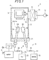
図1は、本発明の実施の一形態であるシリコン窒化膜の形成装置1の構成を簡略化して示す図である。シリコン窒化膜の形成装置1は、基板2を内部空間3に収容する処理容器4と、処理容器4の内部空間3にHMDSガスを供給する第1ガス供給手段5と、処理容器4の内部空間3にN2ガスを供給する第2ガス供給手段6と、第2ガス供給手段6に設けられ処理容器4の内部空間3に供給されるN2ガスをプラズマ励起するプラズマ励起手段7と、基板2を加熱する加熱手段8とを含む。
Hereinafter, preferred embodiments of the present invention will be described in detail with reference to the drawings.
FIG. 1 is a diagram showing a simplified configuration of a silicon nitride
処理容器4は、たとえばステンレス鋼などからなる略直方体形状を有する中空の気密性を備えるチャンバーである。処理容器4の一方の側壁部9には、内部空間3を排気するための排気口10が形成され、排気口10には排気管路11が接続され、排気管路11の排気口10側と反対側の先端には真空ポンプ12(ターボモレキュラーポンプ)が接続される。排気管路11の真空ポンプ12と処理容器4の排気口10との間には、シャッタ13が設けられる。シャッタ13を開き、真空ポンプ12を動作させることによって、内部空間3を排気し低圧にすることができる。またシャッタ13を閉じることによって、処理容器4の内部空間3を密閉空間にすることができる。なお図1では省略されているけれども、処理容器4には、基板2を内部空間3に出入させることの可能な開閉自在な扉が設けられる。
The
処理容器4の内部空間3に収容されるシリコン窒化膜を形成するべき基板2は、たとえばシリコンウェハに回路の形成されるシリコン基板である。基板2を加熱する加熱手段8は、ヒータ14と、ヒータ14で発生される熱を基板2に伝導する熱伝導部材15と、ヒータ14に電力を供給するとともに電力供給のON−OFF制御を行う図示しない制御電源とを含む。ヒータ14は、ニクロム線などの抵抗発熱材料が用いられる。熱伝導部材15に接するように、前述の基板2が装着され、熱伝導部材15を介してヒータ14によって、基板2が室温〜800℃の所望の温度に加熱される。
The
制御電源は、たとえば予め定められる動作プログラムに従う通電時間制御によって基板2の温度制御を行うように構成されてもよく、またたとえば熱伝導部材15の基板2が装着される付近に温度検出器を設け、温度検出器の検出出力を制御電源に入力してON−OFFをフィードバック制御するように構成されてもよい。
The control power supply may be configured to control the temperature of the
本実施の形態では、シリコン窒化膜のシリコン(Si)源として、ヘキサアルキルジシラザン{(CnH2n+1)3SiNHSi(CnH2n+1)3}の1種であるHMDS{(CH3)3SiNHSi(CH3)3}が用いられる。HMDSを処理容器4の内部空間3に供給する第1ガス供給手段5は、HMDSを貯留するHMDS供給源16と、HMDS供給源16から処理容器4に供給されるHMDSガスの流路である第1管路17と、第1管路17のガス流方向下流側の端部に接続されて内部空間3に収容される基板2付近にHMDSガスを噴射するように設けられる第1噴射ノズル18と、HMDS供給源16と第1噴射ノズル18との間の第1管路17に設けられHMDSガスの圧力と流量とを調整する圧力流量調整弁19とを含んで構成される。
In this embodiment, as a silicon (Si) source of the silicon nitride film, HMDS {( 1 ) which is a kind of hexaalkyldisilazane {(C n H 2n + 1 ) 3 SiNHSi (C n H 2n + 1 ) 3 } CH 3 ) 3 SiNHSi (CH 3 ) 3 } is used. The first gas supply means 5 for supplying HMDS to the
HMDS供給源16は、たとえばボンベ状の密閉容器であり、内部には液状のHMDSが貯留され、密閉容器内の液面上に形成される空間には気化し蒸気圧に達するHMDSガスが存在する状態である。第1噴射ノズル18は、噴射孔20が基板2を臨み、噴射孔20から噴射されるHMDSガスが基板2付近に供給されるように処理容器4を構成するフランジ状の底板21に固設される。HMDSガスは、圧力流量調整弁19を開くことによって、前述の真空ポンプ12によって排気されて低圧状態にある内部空間3に吸引される形で、第1噴射ノズル18から基板2付近に向けて噴射供給される。HMDSガスの供給流量は、圧力流量調整弁19の開度によって調整される。
The
なお本実施の形態では、HMDSはその高い蒸気圧を利用してHMDS供給源16内で気化したHMDSガスが処理容器4内に吸引される形で供給されるように構成されるけれども、これに限定されることなく、HMDS供給源16にたとえば窒素(N2)ガスを吹込んでバブリングを生じさせ、吹込んだN2ガスをキャリアガスとしてHMDSガスを処理容器4内に供給するように構成されてもよい。
In the present embodiment, the HMDS is configured to be supplied in such a manner that the HMDS gas vaporized in the
本実施の形態では、シリコン窒化膜の窒素(N)源である窒素化合物としてN2ガスが用いられる。N2ガスを処理容器4の内部空間3に供給する第2ガス供給手段6は、N2ガスを貯留するN2供給源22と、N2供給源22から処理容器4に供給されるN2ガスの流路である第2管路23と、第2管路23のガス流方向下流側の端部に接続されて内部空間3に収容される基板2付近にN2ガスを噴射するように設けられる第2噴射ノズル24と、N2供給源22と第2噴射ノズル24との間の第2管路23に設けられN2ガスの圧力と流量とを調整する圧力流量調整弁25とを含んで構成される。
In the present embodiment, N 2 gas is used as a nitrogen compound that is a nitrogen (N) source of the silicon nitride film. N 2 for supplying gas to the
N2供給源22は、たとえばボンベ状の密閉容器であり、内部にはN2ガスが貯留されている。第2噴射ノズル24は、噴射孔26が基板2を臨み、噴射孔26から噴射されるN2ガスが基板2付近に供給されるように処理容器4を構成するフランジ状の底板21に固設される。N2ガスの供給流量は、圧力流量調整弁25の開度によって調整される。
The N 2 supply source 22 is, for example, a cylinder-like sealed container, in which N 2 gas is stored. The
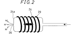
図2は、第2ガス供給手段6の第2噴射ノズル24部分の拡大図である。図2に示すように、第2ガス供給手段6のガス供給部である第2噴射ノズル24は、オリフィス構造を有する。第2噴射ノズル24の基板2を臨む先端部24aに形成される噴射孔26は、第2噴射ノズル24から流体であるN2ガスを噴出させる孔、すなわちオリフィスである。第2噴射ノズル24は、処理容器4の内部空間3にN2ガスを供給する噴射孔26であるオリフィス部の圧力が、処理容器4の内部空間3の圧力、すなわち第1ガス供給手段5から内部空間3に供給されたHMDSの圧力よりも高くなるように構成される。
FIG. 2 is an enlarged view of the
この第2噴射ノズル24の第2管路23に接続される側の端部付近には、プラズマ励起手段7が接続される。プラズマ励起手段7は、高周波発振器27と、マッチングユニット28とを含んで構成される。プラズマ励起手段7には誘動結合型R.F.セルが設けられ、プラズマ励起手段7による高周波電圧を、第2噴射ノズル24に設けられるヘリカルアンテナ29に印加することによって、第2噴射ノズル24中を流過するN2ガスがプラズマ励起されて活性種(図2中ではN*で表記)が形成される。したがって、第2噴射ノズル24の噴射孔26から噴射されて基板2付近に供給されるN2ガスは、正確にはプラズマ励起されて形成される活性種を含むガスのことである。
The plasma excitation means 7 is connected to the vicinity of the end of the
前述のように、第1ガス供給手段5から内部空間3に供給されたHMDSの圧力は、オリフィス構造を有する第2噴射ノズル24から供給されている活性種を含むN2ガスの圧力よりも低いので、HMDSガスが内部空間3から第2噴射ノズル24内へ逆流することが防止される。したがって、HMDSガスは、プラズマ励起手段7による励起や解離を生じることがない。
As described above, the pressure of HMDS supplied from the first gas supply means 5 to the
第1噴射ノズル18から基板2付近に供給されるHMDSは、第2噴射ノズル24から基板2付近に供給されるプラズマ励起されて形成される活性種からエネルギを受取って解離する。HMDSの解離によって形成されるSiが、さらに活性種と反応し、反応生成物が基板2の表面に堆積されてシリコン窒化膜が形成される。HMDSは、活性種からエネルギを与えられて解離するのであって、直接プラズマ励起されて解離するものではないので、HMDSの解離によって生じるCおよびHは、過剰に活性化することがない。
The HMDS supplied from the
このようにシリコン窒化膜の形成装置1は、シリコン窒化膜の構成要素の一方であるN源のみをプラズマ励起させて供給し、シリコン窒化膜の構成要素の他方であるSi源のHMDSをプラズマ励起させることなく供給できるという特徴を有する。
As described above, the silicon nitride
一般的なPECVD装置では、処理容器内に一対の電極を備えて処理容器内で放電するので、処理容器内に供給されたN2ガス、NH3ガスおよびHMDSが共にプラズマ励起される。したがって、シリコン窒化膜の堆積効率はよいけれども、HMDSもプラズマ励起されてしまうので、SiとともにCおよびHも同様に活性化し、活性種との反応生成物として基板2の表面に堆積される。このようにして形成されるシリコン窒化膜は、CおよびHによって汚染されることになり、膜性能の低下を生じる。
In a general PECVD apparatus, a pair of electrodes are provided in a processing container and discharge is performed in the processing container. Therefore, N 2 gas, NH 3 gas and HMDS supplied into the processing container are all excited by plasma. Therefore, although the deposition efficiency of the silicon nitride film is good, HMDS is also plasma-excited, so C and H are activated in the same manner as Si, and are deposited on the surface of the
しかしながら、本発明のシリコン窒化膜の形成装置1では、前述のようにプラズマ励起されたN源と、プラズマ励起されないSi源であるHMDSとを分離して個別に供給することができるので、HMDSに含まれるCおよびHの活性化が抑制され、反応生成物として形成されるシリコン窒化膜中のCおよびH含有量の低減が実現される。またN源であるN2ガスをプラズマ励起させるけれども、Si源であるHMDSをプラズマ励起させないので、N源とSi源との両者をプラズマ励起させる場合に比べて若干シリコン窒化膜の堆積効率は低下するものの、熱CVD法に比べると高い堆積効率が維持される。
However, in the silicon nitride
シリコン窒化膜の形成装置1によって形成されるシリコン窒化膜の組成は、主としてSi3N4であるけれども、このシリコン窒化膜におけるSiとNとの組成比は、基板2付近に供給するHMDSおよびN2ガスの流量比を調整することによって、制御することが可能である。またシリコン窒化膜の形成装置1では、シリコン窒化膜の構成要素であるSiおよびNの両者を第1および第2ガス供給手段5,6によって供給するので、シリコン窒化膜の形成に際し、基板のSiとの反応を必須の要件としていない。したがって、基板の組成にSiを含有しなければならないという制約がないので、シリコン窒化膜を形成するべき基板は、シリコンウェハに限定されることなく、ガリウムヒ素(GaAs)などその他の組成の基板であってもよい。
Although the composition of the silicon nitride film formed by the silicon nitride
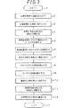
図3は、シリコン窒化膜の形成装置1を用いて基板2上にシリコン窒化膜を形成する動作を説明するフローチャートである。図3を参照して基板2上にシリコン窒化膜を形成する動作を説明する。
FIG. 3 is a flowchart for explaining the operation of forming a silicon nitride film on the
ステップa1のスタートでは、シリコン窒化膜の形成装置1を準備するとともに、第1および第2ガス供給手段5,6には、HMDSおよびN2ガスが準備されている状態である。ステップa2では、基板2を、処理容器4の内部空間3に搬入し、熱伝導部材15の予め定められる位置に装着する。ステップa3では、シャッタ13を開き真空ポンプ12を動作させて、処理容器4内を排気する。シャッタ13の開口度によって処理容器4内の真空度を調整し、予め定められる圧力にする。
At the start of step a1, the silicon nitride
ステップa4では、基板2を加熱手段8によって予め定められる温度に加熱する。基板2の加熱は、HMDSガスおよびN2ガスの供給される前に行われてもよい。ステップa5では、第2ガス供給手段6によって、処理容器4内にプラズマ励起手段7でプラズマ励起されたN2ガスを供給する。ここで、N2ガスは、より正確にはプラズマ励起されて形成される活性種を含むガスである。ステップa6では、第1ガス供給手段5によって、処理容器4内にHMDSガスを供給する。
In step a4, the
ステップa7では、予め求められたシリコン窒化膜の堆積厚みと処理時間との関係に基づいて設定される時間が経過するまで、基板2の加熱とHMDSガスおよびN2ガスの供給とを継続し、HMDSガスとプラズマ励起によって形成される活性種との反応生成物を、基板2の表面に堆積させてシリコン窒化膜を形成する。ステップa8では、処理容器4内へのHMDSガスの供給を停止する。ステップa9では、処理容器4内へのN2ガスの供給を停止する。ステップa10では、前述の設定される時間が経過した後、基板2の加熱を停止して冷却する。
In step a7, the heating of the
ステップa11では、前述の図1における図示が省略されているけれども、たとえば処理容器4に設けられる大気開放弁を開放して処理容器4内の圧力を大気圧に調整する。ステップa12では、処理容器4から基板2を搬出してステップa13に進み一連のシリコン窒化膜の形成動作を終了する。
In step a11, although the illustration in FIG. 1 is omitted, for example, the atmospheric release valve provided in the
(実施例)
以下に本発明の実施例を説明する。
シリコン窒化膜の形成装置1を準備し、シリコン窒化膜のSi源にHMDSを用い、N源にN2ガスを用いて、シリコンウェハの基板上にシリコン窒化膜を形成した。シリコン窒化膜形成に用いた条件をまとめて表1に示す。なお、形成装置1に備わる処理容器4の内部空間3の容積は大略1000L(リットル)であった。
(Example)
Examples of the present invention will be described below.
A silicon nitride
表1に示す条件にて、HMDSガスと、N2ガスがプラズマ励起されて形成された活性種との反応生成物を、3hour継続してシリコンウェハ上に堆積させてシリコン窒化膜を形成した。形成されたシリコン窒化膜の組成を、XPS(X-ray Photoelectron Spectroscopy)およびフーリエ変換赤外分光光度計(FT−IR:Fourier Transform Infra Red)にて測定した。またシリコン窒化膜の比誘電率をインピーダンス計(WAYNEKERR社製;Precision Component Analyzer6425)で測定し、屈折率をエリプソメーター(溝尻光学工業所社製;DVA−FL型)で測定した。 Under the conditions shown in Table 1, reaction products of HMDS gas and active species formed by plasma excitation of N 2 gas were continuously deposited on a silicon wafer for 3 hours to form a silicon nitride film. The composition of the formed silicon nitride film was measured with an XPS (X-ray Photoelectron Spectroscopy) and a Fourier Transform Infrared Spectrometer (FT-IR). Further, the relative dielectric constant of the silicon nitride film was measured with an impedance meter (manufactured by WAYNEKER; Precision Component Analyzer 6425), and the refractive index was measured with an ellipsometer (manufactured by Mizojiri Optical Industry Co., Ltd .; DVA-FL type).
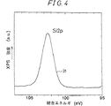
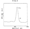
図4はXPSによるシリコン窒化膜中のSiの分析結果を示す図であり、図5はXPSによるシリコン窒化膜中のNの分析結果を示す図である。図4中のライン31に明らかなように、Siの存在を示す結合エネルギにおいて明瞭なピークが認められた。同様に図5中のライン32に明らかなように、Nの存在を示す結合エネルギにおいて明瞭なピークが認められた。このことから、シリコンウェハ上に形成された膜中には、SiおよびNの含有されること、すなわちシリコン窒化膜の形成されていることが確認された。
FIG. 4 is a diagram showing the analysis result of Si in the silicon nitride film by XPS, and FIG. 5 is a diagram showing the analysis result of N in the silicon nitride film by XPS. As apparent from the
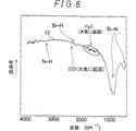
図6は、FT−IRによるシリコン窒化膜の分析結果を示す図である。FT−IRによるシリコン窒化膜の分析結果は、横軸に波数、縦軸に透過率をとって示され、図6中にライン33で示すスペクトルが、分析結果である。スペクトルから、シリコン窒化膜には、Si−Nの結合の存在が確認された。またスペクトルからごくわずかながらHの取込まれていることが確認された。一方C−Hは、FT−IRの検出限界以下であった。膜中にC−Hを含むと、非常に不安定になり、膜特性の経時変化を起こしやすくなる。また膜密度の緻密性も失われる。本方法により堆積されたシリコン窒化膜は、緻密で経時変化が起こりにくい膜であると考えられる。
FIG. 6 is a diagram showing an analysis result of the silicon nitride film by FT-IR. The analysis result of the silicon nitride film by FT-IR is shown by taking the wave number on the horizontal axis and the transmittance on the vertical axis, and the spectrum indicated by the
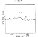
図7は、XPSによるシリコン窒化膜中のC(炭素)の分析結果を示す図である。図7中のライン34に示すように、Cが観測されなかったことから、膜中へのCの混入は少ない。
FIG. 7 is a diagram showing an analysis result of C (carbon) in the silicon nitride film by XPS. As shown by the
シリコン窒化膜の比誘電率は、7.6であり、他の絶縁皮膜たとえばシリコン酸化膜の比誘電率:4に比べて優れた値であった。屈折率は、1.8〜2.0であった。シリコン窒化膜形成時におけるHMDSガスの流量とN2ガスの流量との比を調整することによって、シリコン窒化膜SiとNiとの組成比を調整し、ある程度屈折率を制御することができる。このように所望の屈折率を有するシリコン窒化膜を形成することによって、たとえば導波路を形成する光学素子などへの利用可能性が期待できる。 The relative dielectric constant of the silicon nitride film was 7.6, which was an excellent value compared to the relative dielectric constant: 4 of other insulating films such as a silicon oxide film. The refractive index was 1.8 to 2.0. By adjusting the ratio of the flow rate of HMDS gas and the flow rate of N 2 gas at the time of forming the silicon nitride film, the composition ratio of the silicon nitride film Si and Ni can be adjusted, and the refractive index can be controlled to some extent. Thus, by forming a silicon nitride film having a desired refractive index, it can be expected to be applicable to, for example, an optical element that forms a waveguide.
以上に述べたように本実施の形態では、シリコン窒化膜のSi源にHMDSが用いられるけれども、これに限定されることなく、ヘキサアルキルジシラザンに属する他の有機シラン系化合物が用いられてもよい。また窒素化合物には、N2が用いられるけれども、これに限定されることなく、NH3が用いられてもよく、さらにN2および/またはHN3に加え、H2,He,Ar,Xe,Neなどからなる群より選択される1種以上のガスを含むように構成されてもよい。またプラズマ励起手段7には、高周波電界を印加して放電する手段が用いられるけれども、これに限定されることなく、他の手段であってもよい。また基板2は、加熱手段8によって加熱されるように構成されるけれども、基板2は加熱されない構成であってもよい。但しシリコン窒化膜の堆積効率を少しでも向上する観点からは、加熱する方が好ましい。
As described above, in the present embodiment, HMDS is used for the Si source of the silicon nitride film, but the present invention is not limited to this, and other organosilane compounds belonging to hexaalkyldisilazane may be used. Good. In addition, N 2 is used as the nitrogen compound, but NH 3 may be used without being limited thereto, and in addition to N 2 and / or HN 3 , H 2 , He, Ar, Xe, You may comprise so that 1 or more types of gas selected from the group which consists of Ne etc. may be included. Moreover, although the means for discharging by applying a high frequency electric field is used for the plasma excitation means 7, it is not limited to this and other means may be used. Further, although the
本発明は、その精神または主要な特徴から逸脱することなく、他のいろいろな形態で実施できる。従って、前述の実施形態はあらゆる点で単なる例示に過ぎず、本発明の範囲は特許請求の範囲に示すものであって、明細書本文には何ら拘束されない。さらに、特許請求の範囲に属する変形や変更は全て本発明の範囲内のものである。 The present invention can be implemented in various other forms without departing from the spirit or main features thereof. Accordingly, the above-described embodiment is merely an example in all respects, and the scope of the present invention is shown in the claims, and is not limited to the text of the specification. Further, all modifications and changes belonging to the scope of the claims are within the scope of the present invention.
1 シリコン窒化膜の形成装置
2 基板
3 内部空間
4 処理容器
5 第1ガス供給手段
6 第2ガス供給手段
7 プラズマ励起手段
8 加熱手段
12 真空ポンプ
13 シャッタ
DESCRIPTION OF
Claims (4)
前記基板の収容される前記処理容器内に、前記処理容器の底板に固設される噴射ノズルから上方の前記基板に向かって、ヘキサメチルジシラザン{(CH3)3SiNHSi(CH3)3}ガスとプラズマ励起されたN 2 またはNH 3 のうち少なくともいずれか1種の窒素化合物からなるガスとを、基板付近における反応生成物が生成される領域の圧力よりも前記窒素化合物がプラズマ励起される領域の圧力の方が高くなるようにして供給し、
前記ヘキサメチルジシラザンガスと前記プラズマ励起された窒素化合物からなるガスとの反応生成物を前記基板上に堆積させてシリコン窒化膜を形成することを特徴とするシリコン窒化膜の形成方法。The substrate is accommodated in the internal space of the processing container,
Into the processing chamber to be accommodated in the substrate, upward of the substrate from the injection nozzle which is fixed to the bottom plate of the processing container, hexamethyl disilazane {(CH 3) 3 SiNHSi ( CH 3) 3} Gas A region in which the nitrogen compound is plasma-excited with a gas composed of at least any one of N 2 and NH 3 plasma-excited and a pressure in a region in the vicinity of the substrate where a reaction product is generated. Supply so that the pressure of is higher ,
Method of forming a silicon nitride film and forming the hexamethyl Jishirazangasu and the silicon nitride film and the reaction product is deposited on the substrate with a gas consisting of plasma-excited nitrogen compounds.
前記基板の収容される前記処理容器内に、前記処理容器の底板に固設される噴射ノズルから上方の前記基板に向かって、第一噴射ノズルでヘキサメチルジシラザン{(CH3)3SiNHSi(CH3)3}ガスを供給し、オリフィス構造を有する第二噴射ノズルでプラズマ励起されたN 2 またはNH 3 のうち少なくともいずれか1種の窒素化合物からなるガスを供給し、
前記ヘキサメチルジシラザンガスと前記プラズマ励起された窒素化合物からなるガスとの反応生成物を前記基板上に堆積させてシリコン窒化膜を形成することを特徴とするシリコン窒化膜の形成方法。The substrate is accommodated in the internal space of the processing container,
Into the processing chamber to be accommodated in the substrate, upward of the substrate from the injection nozzle which is fixed to the bottom plate of the processing chamber, first injection nozzle with hexamethyl disilazane {(CH 3) 3 SiNHSi ( CH 3 ) 3 } gas is supplied, and a gas comprising at least one nitrogen compound of N 2 or NH 3 plasma-excited by a second injection nozzle having an orifice structure is supplied,
Method of forming a silicon nitride film and forming the hexamethyl Jishirazangasu and the silicon nitride film and the reaction product is deposited on the substrate with a gas consisting of plasma-excited nitrogen compounds.
前記基板を内部空間に収容する処理容器と、
噴射孔が基板を臨み、噴射孔から上方に向かって噴射されるヘキサアルキルジシラザンガスが基板付近に供給されるように、前記処理容器の底板に固設される第1噴射ノズルを有し、前記処理容器の内部空間にヘキサアルキルジシラザンガスを供給する第1ガス供給手段と、
噴射孔が基板を臨み、噴射孔から上方に向かって噴射される窒素化合物からなるガスが基板付近に供給されるように、前記処理容器の底板に固設される第2噴射ノズルを有し、前記処理容器の内部空間に窒素化合物からなるガスを供給する第2ガス供給手段と、
前記第2ガス供給手段に設けられ、前記処理容器の内部空間に供給される窒素化合物からなるガスをプラズマ励起するプラズマ励起手段と、
前記基板を加熱する加熱手段とを含み、
前記処理容器の内部空間にガスを供給する前記第2ガス供給手段のガス供給部は、オリフィス構造を有し、
前記ヘキサアルキルジシラザンは、ヘキサメチルジシラザンであり、
前記窒素化合物は、N2またはNH3のうち少なくともいずれか1種であることを特徴とするシリコン窒化膜の形成装置。A silicon nitride film forming apparatus for forming a silicon nitride film on a surface of a substrate,
A processing container for accommodating the substrate in an internal space;
A first injection nozzle fixed to the bottom plate of the processing vessel so that the injection hole faces the substrate and hexaalkyldisilazane gas injected upward from the injection hole is supplied to the vicinity of the substrate; First gas supply means for supplying hexaalkyldisilazane gas to the internal space of the processing vessel;
A second injection nozzle fixed to the bottom plate of the processing vessel so that the injection hole faces the substrate and a gas composed of a nitrogen compound injected upward from the injection hole is supplied to the vicinity of the substrate; Second gas supply means for supplying a gas composed of a nitrogen compound to the internal space of the processing container;
Plasma excitation means provided in the second gas supply means, for plasma-exciting a gas comprising a nitrogen compound supplied to the internal space of the processing vessel;
Heating means for heating the substrate,
The gas supply part of the second gas supply means for supplying gas to the internal space of the processing container has an orifice structure,
The hexaalkyldisilazane is hexamethyldisilazane;
The silicon nitride film forming apparatus according to claim 1 , wherein the nitrogen compound is at least one of N 2 and NH 3 .
Applications Claiming Priority (3)
| Application Number | Priority Date | Filing Date | Title |
|---|---|---|---|
| JP2002199122 | 2002-07-08 | ||
| JP2002199122 | 2002-07-08 | ||
| PCT/JP2003/008552 WO2004006321A1 (en) | 2002-07-08 | 2003-07-04 | Method and apparatus for forming nitrided silicon film |
Publications (2)
| Publication Number | Publication Date |
|---|---|
| JPWO2004006321A1 JPWO2004006321A1 (en) | 2005-11-10 |
| JP4197319B2 true JP4197319B2 (en) | 2008-12-17 |
Family
ID=30112450
Family Applications (1)
| Application Number | Title | Priority Date | Filing Date |
|---|---|---|---|
| JP2004519275A Expired - Fee Related JP4197319B2 (en) | 2002-07-08 | 2003-07-04 | Method and apparatus for forming silicon nitride film |
Country Status (5)
| Country | Link |
|---|---|
| US (1) | US20050255713A1 (en) |
| JP (1) | JP4197319B2 (en) |
| KR (1) | KR100623562B1 (en) |
| AU (1) | AU2003281403A1 (en) |
| WO (1) | WO2004006321A1 (en) |
Families Citing this family (13)
| Publication number | Priority date | Publication date | Assignee | Title |
|---|---|---|---|---|
| DE10350752A1 (en) * | 2003-10-30 | 2005-06-09 | Infineon Technologies Ag | A method of forming a dielectric on a copper-containing metallization and capacitor assembly |
| US20050214456A1 (en) * | 2004-03-29 | 2005-09-29 | Donghul Lu | Enhanced dielectric layers using sequential deposition |
| US20060192183A1 (en) * | 2005-02-28 | 2006-08-31 | Andreas Klyszcz | Metal ink, method of preparing the metal ink, substrate for display, and method of manufacturing the substrate |
| JP4228150B2 (en) * | 2005-03-23 | 2009-02-25 | 東京エレクトロン株式会社 | Film forming apparatus, film forming method, and storage medium |
| DE102006035563A1 (en) * | 2006-07-27 | 2008-01-31 | Kimes, Karin | Silane-free plasma-assisted CVD deposition of silicon nitride as an anti-reflective film and hydrogen passivation of silicon cell-based photocells |
| US7638170B2 (en) * | 2007-06-21 | 2009-12-29 | Asm International N.V. | Low resistivity metal carbonitride thin film deposition by atomic layer deposition |
| US8017182B2 (en) * | 2007-06-21 | 2011-09-13 | Asm International N.V. | Method for depositing thin films by mixed pulsed CVD and ALD |
| US7867923B2 (en) * | 2007-10-22 | 2011-01-11 | Applied Materials, Inc. | High quality silicon oxide films by remote plasma CVD from disilane precursors |
| JP5883049B2 (en) * | 2014-03-04 | 2016-03-09 | 株式会社日立国際電気 | Semiconductor device manufacturing method, substrate processing apparatus, program, and recording medium |
| KR101909110B1 (en) * | 2016-08-18 | 2018-10-18 | 피에스케이 주식회사 | Substrate treating method |
| JP6777614B2 (en) * | 2017-09-26 | 2020-10-28 | 株式会社Kokusai Electric | Semiconductor device manufacturing methods, substrate processing devices, and programs |
| US20190386256A1 (en) * | 2018-06-18 | 2019-12-19 | Universal Display Corporation | Sequential material sources for thermally challenged OLED materials |
| JP7779632B2 (en) * | 2022-04-18 | 2025-12-03 | 東京エレクトロン株式会社 | Film forming method |
Family Cites Families (11)
| Publication number | Priority date | Publication date | Assignee | Title |
|---|---|---|---|---|
| JPS54123599A (en) * | 1978-03-17 | 1979-09-25 | Toshiba Corp | Forming method for silicon nitride film |
| JPS6333575A (en) * | 1986-07-28 | 1988-02-13 | Nippon Soken Inc | Electron cyclotron plasma cvd device |
| KR920002864B1 (en) * | 1987-07-20 | 1992-04-06 | 가부시기가이샤 히다찌세이사꾸쇼 | Apparatus for treating matrial by using plasma |
| JPH01298164A (en) * | 1988-05-25 | 1989-12-01 | Canon Inc | Formation of functional deposit film |
| JP2861600B2 (en) * | 1992-03-04 | 1999-02-24 | 日本電気株式会社 | Method and apparatus for selective growth of silicon epitaxial film |
| JPH05263255A (en) * | 1992-03-19 | 1993-10-12 | Hitachi Electron Eng Co Ltd | Plasma cvd device |
| JPH07335395A (en) * | 1994-04-13 | 1995-12-22 | Rikagaku Kenkyusho | Plasma generation method and film forming method, etching method, semiconductor deposition method and doping method using the same |
| JPH07288237A (en) * | 1994-04-15 | 1995-10-31 | Nippon Steel Corp | Plasma excitation cell device |
| JPH08321504A (en) * | 1995-05-24 | 1996-12-03 | Ulvac Japan Ltd | Mocvd equipment for nitride |
| JPH0941147A (en) * | 1995-07-31 | 1997-02-10 | Canon Inc | Plasma CVD method |
| JPH11265883A (en) * | 1998-03-17 | 1999-09-28 | Asahi Kasei Micro Syst Co Ltd | Semiconductor manufacturing equipment and process tube for reaction chamber |
-
2003
- 2003-07-04 US US10/520,815 patent/US20050255713A1/en not_active Abandoned
- 2003-07-04 JP JP2004519275A patent/JP4197319B2/en not_active Expired - Fee Related
- 2003-07-04 WO PCT/JP2003/008552 patent/WO2004006321A1/en not_active Ceased
- 2003-07-04 KR KR1020057000364A patent/KR100623562B1/en not_active Expired - Fee Related
- 2003-07-04 AU AU2003281403A patent/AU2003281403A1/en not_active Abandoned
Also Published As
| Publication number | Publication date |
|---|---|
| KR100623562B1 (en) | 2006-09-13 |
| AU2003281403A1 (en) | 2004-01-23 |
| WO2004006321A1 (en) | 2004-01-15 |
| JPWO2004006321A1 (en) | 2005-11-10 |
| KR20050021446A (en) | 2005-03-07 |
| US20050255713A1 (en) | 2005-11-17 |
Similar Documents
| Publication | Publication Date | Title |
|---|---|---|
| US10361088B2 (en) | Techniques and systems for continuous-flow plasma enhanced atomic layer deposition (PEALD) | |
| JP4197319B2 (en) | Method and apparatus for forming silicon nitride film | |
| US10804098B2 (en) | Systems and methods for thin-film deposition of metal oxides using excited nitrogen-oxygen species | |
| US7531467B2 (en) | Manufacturing method of semiconductor device and substrate processing apparatus | |
| KR100988096B1 (en) | Plasma Cyclic Chemical Vapor Deposition of Silicon-Containing Films | |
| US8877655B2 (en) | Systems and methods for thin-film deposition of metal oxides using excited nitrogen-oxygen species | |
| CN101048853B (en) | Precursor for film formation and method for forming ruthenium-containing film | |
| KR101293041B1 (en) | Method of manufacturing semiconductor device, method of processing substrate, substrate processing apparatus and computer-readable medium having thereon program performing function embodying the same | |
| KR101726946B1 (en) | Manufacturing method of semiconductor device, substrate processing apparatus and program | |
| US20050223982A1 (en) | Apparatus and method for depositing thin film on wafer using remote plasma | |
| US20050070126A1 (en) | System and method for forming multi-component dielectric films | |
| US20110070380A1 (en) | Systems and methods for thin-film deposition of metal oxides using excited nitrogen-oxygen species | |
| JP3700177B2 (en) | Atmospheric pressure plasma surface treatment equipment | |
| CN110402477A (en) | Selective growth of silicon oxide or silicon nitride on silicon surfaces in the presence of silicon oxide | |
| JP2005079141A (en) | Plasma cvd system | |
| US11087959B2 (en) | Techniques for a hybrid design for efficient and economical plasma enhanced atomic layer deposition (PEALD) and plasma enhanced chemical vapor deposition (PECVD) | |
| WO2004066377A1 (en) | Method of cvd for forming silicon nitride film on substrate | |
| CN101014730A (en) | System and method for forming multi-component dielectric films | |
| US20170011908A1 (en) | Method of manufacturing semiconductor device, substrate processing apparatus, and recording medium | |
| KR20110118564A (en) | Manufacturing Method of Substrate Processing Apparatus and Semiconductor Device | |
| KR20160031413A (en) | Method and apparatus of manufacturing semiconductor device, and computer program | |
| CN112458435B (en) | Atomic layer deposition equipment and cleaning method | |
| JP4624991B2 (en) | Method and apparatus for forming oxynitride film | |
| TW306937B (en) | ||
| JPH05263255A (en) | Plasma cvd device |
Legal Events
| Date | Code | Title | Description |
|---|---|---|---|
| A131 | Notification of reasons for refusal |
Free format text: JAPANESE INTERMEDIATE CODE: A131 Effective date: 20070710 |
|
| A521 | Request for written amendment filed |
Free format text: JAPANESE INTERMEDIATE CODE: A523 Effective date: 20070910 |
|
| A711 | Notification of change in applicant |
Free format text: JAPANESE INTERMEDIATE CODE: A711 Effective date: 20070910 |
|
| A521 | Request for written amendment filed |
Free format text: JAPANESE INTERMEDIATE CODE: A523 Effective date: 20070918 |
|
| A131 | Notification of reasons for refusal |
Free format text: JAPANESE INTERMEDIATE CODE: A131 Effective date: 20071211 |
|
| A02 | Decision of refusal |
Free format text: JAPANESE INTERMEDIATE CODE: A02 Effective date: 20080311 |
|
| A521 | Request for written amendment filed |
Free format text: JAPANESE INTERMEDIATE CODE: A523 Effective date: 20080512 |
|
| A521 | Request for written amendment filed |
Free format text: JAPANESE INTERMEDIATE CODE: A821 Effective date: 20080512 |
|
| RD02 | Notification of acceptance of power of attorney |
Free format text: JAPANESE INTERMEDIATE CODE: A7422 Effective date: 20080626 |
|
| A521 | Request for written amendment filed |
Free format text: JAPANESE INTERMEDIATE CODE: A821 Effective date: 20080701 |
|
| RD04 | Notification of resignation of power of attorney |
Free format text: JAPANESE INTERMEDIATE CODE: A7424 Effective date: 20080701 |
|
| A521 | Request for written amendment filed |
Free format text: JAPANESE INTERMEDIATE CODE: A523 Effective date: 20080717 |
|
| A911 | Transfer to examiner for re-examination before appeal (zenchi) |
Free format text: JAPANESE INTERMEDIATE CODE: A911 Effective date: 20080723 |
|
| TRDD | Decision of grant or rejection written | ||
| A01 | Written decision to grant a patent or to grant a registration (utility model) |
Free format text: JAPANESE INTERMEDIATE CODE: A01 Effective date: 20080924 |
|
| A01 | Written decision to grant a patent or to grant a registration (utility model) |
Free format text: JAPANESE INTERMEDIATE CODE: A01 |
|
| A61 | First payment of annual fees (during grant procedure) |
Free format text: JAPANESE INTERMEDIATE CODE: A61 Effective date: 20080925 |
|
| FPAY | Renewal fee payment (event date is renewal date of database) |
Free format text: PAYMENT UNTIL: 20111010 Year of fee payment: 3 |
|
| R150 | Certificate of patent or registration of utility model |
Free format text: JAPANESE INTERMEDIATE CODE: R150 |
|
| FPAY | Renewal fee payment (event date is renewal date of database) |
Free format text: PAYMENT UNTIL: 20111010 Year of fee payment: 3 |
|
| FPAY | Renewal fee payment (event date is renewal date of database) |
Free format text: PAYMENT UNTIL: 20131010 Year of fee payment: 5 |
|
| LAPS | Cancellation because of no payment of annual fees |