JP4092827B2 - 表示装置 - Google Patents
表示装置 Download PDFInfo
- Publication number
- JP4092827B2 JP4092827B2 JP30144899A JP30144899A JP4092827B2 JP 4092827 B2 JP4092827 B2 JP 4092827B2 JP 30144899 A JP30144899 A JP 30144899A JP 30144899 A JP30144899 A JP 30144899A JP 4092827 B2 JP4092827 B2 JP 4092827B2
- Authority
- JP
- Japan
- Prior art keywords
- oeld
- display device
- thin film
- signal line
- light emitting
- Prior art date
- Legal status (The legal status is an assumption and is not a legal conclusion. Google has not performed a legal analysis and makes no representation as to the accuracy of the status listed.)
- Expired - Lifetime
Links
- 238000005401 electroluminescence Methods 0.000 claims description 10
- 238000005070 sampling Methods 0.000 claims description 9
- 239000010409 thin film Substances 0.000 claims description 9
- 238000010586 diagram Methods 0.000 description 13
- 238000000034 method Methods 0.000 description 12
- 239000007788 liquid Substances 0.000 description 10
- 239000007791 liquid phase Substances 0.000 description 6
- 229920000642 polymer Polymers 0.000 description 3
- 230000002940 repellent Effects 0.000 description 3
- 239000005871 repellent Substances 0.000 description 3
- 239000011248 coating agent Substances 0.000 description 2
- 238000000576 coating method Methods 0.000 description 2
- 230000014759 maintenance of location Effects 0.000 description 2
- 230000000704 physical effect Effects 0.000 description 2
- 238000004528 spin coating Methods 0.000 description 2
- 239000000758 substrate Substances 0.000 description 2
- 230000000694 effects Effects 0.000 description 1
- 238000004020 luminiscence type Methods 0.000 description 1
- 238000004519 manufacturing process Methods 0.000 description 1
- 239000000463 material Substances 0.000 description 1
Images


Classifications
-
- H—ELECTRICITY
- H10—SEMICONDUCTOR DEVICES; ELECTRIC SOLID-STATE DEVICES NOT OTHERWISE PROVIDED FOR
- H10K—ORGANIC ELECTRIC SOLID-STATE DEVICES
- H10K59/00—Integrated devices, or assemblies of multiple devices, comprising at least one organic light-emitting element covered by group H10K50/00
- H10K59/10—OLED displays
- H10K59/12—Active-matrix OLED [AMOLED] displays
- H10K59/121—Active-matrix OLED [AMOLED] displays characterised by the geometry or disposition of pixel elements
-
- G—PHYSICS
- G06—COMPUTING; CALCULATING OR COUNTING
- G06T—IMAGE DATA PROCESSING OR GENERATION, IN GENERAL
- G06T5/00—Image enhancement or restoration
-
- G—PHYSICS
- G09—EDUCATION; CRYPTOGRAPHY; DISPLAY; ADVERTISING; SEALS
- G09G—ARRANGEMENTS OR CIRCUITS FOR CONTROL OF INDICATING DEVICES USING STATIC MEANS TO PRESENT VARIABLE INFORMATION
- G09G3/00—Control arrangements or circuits, of interest only in connection with visual indicators other than cathode-ray tubes
- G09G3/20—Control arrangements or circuits, of interest only in connection with visual indicators other than cathode-ray tubes for presentation of an assembly of a number of characters, e.g. a page, by composing the assembly by combination of individual elements arranged in a matrix no fixed position being assigned to or needed to be assigned to the individual characters or partial characters
- G09G3/2007—Display of intermediate tones
- G09G3/2074—Display of intermediate tones using sub-pixels
-
- G—PHYSICS
- G09—EDUCATION; CRYPTOGRAPHY; DISPLAY; ADVERTISING; SEALS
- G09G—ARRANGEMENTS OR CIRCUITS FOR CONTROL OF INDICATING DEVICES USING STATIC MEANS TO PRESENT VARIABLE INFORMATION
- G09G3/00—Control arrangements or circuits, of interest only in connection with visual indicators other than cathode-ray tubes
- G09G3/20—Control arrangements or circuits, of interest only in connection with visual indicators other than cathode-ray tubes for presentation of an assembly of a number of characters, e.g. a page, by composing the assembly by combination of individual elements arranged in a matrix no fixed position being assigned to or needed to be assigned to the individual characters or partial characters
- G09G3/22—Control arrangements or circuits, of interest only in connection with visual indicators other than cathode-ray tubes for presentation of an assembly of a number of characters, e.g. a page, by composing the assembly by combination of individual elements arranged in a matrix no fixed position being assigned to or needed to be assigned to the individual characters or partial characters using controlled light sources
- G09G3/30—Control arrangements or circuits, of interest only in connection with visual indicators other than cathode-ray tubes for presentation of an assembly of a number of characters, e.g. a page, by composing the assembly by combination of individual elements arranged in a matrix no fixed position being assigned to or needed to be assigned to the individual characters or partial characters using controlled light sources using electroluminescent panels
- G09G3/32—Control arrangements or circuits, of interest only in connection with visual indicators other than cathode-ray tubes for presentation of an assembly of a number of characters, e.g. a page, by composing the assembly by combination of individual elements arranged in a matrix no fixed position being assigned to or needed to be assigned to the individual characters or partial characters using controlled light sources using electroluminescent panels semiconductive, e.g. using light-emitting diodes [LED]
- G09G3/3208—Control arrangements or circuits, of interest only in connection with visual indicators other than cathode-ray tubes for presentation of an assembly of a number of characters, e.g. a page, by composing the assembly by combination of individual elements arranged in a matrix no fixed position being assigned to or needed to be assigned to the individual characters or partial characters using controlled light sources using electroluminescent panels semiconductive, e.g. using light-emitting diodes [LED] organic, e.g. using organic light-emitting diodes [OLED]
- G09G3/3225—Control arrangements or circuits, of interest only in connection with visual indicators other than cathode-ray tubes for presentation of an assembly of a number of characters, e.g. a page, by composing the assembly by combination of individual elements arranged in a matrix no fixed position being assigned to or needed to be assigned to the individual characters or partial characters using controlled light sources using electroluminescent panels semiconductive, e.g. using light-emitting diodes [LED] organic, e.g. using organic light-emitting diodes [OLED] using an active matrix
- G09G3/3258—Control arrangements or circuits, of interest only in connection with visual indicators other than cathode-ray tubes for presentation of an assembly of a number of characters, e.g. a page, by composing the assembly by combination of individual elements arranged in a matrix no fixed position being assigned to or needed to be assigned to the individual characters or partial characters using controlled light sources using electroluminescent panels semiconductive, e.g. using light-emitting diodes [LED] organic, e.g. using organic light-emitting diodes [OLED] using an active matrix with pixel circuitry controlling the voltage across the light-emitting element
-
- G—PHYSICS
- G09—EDUCATION; CRYPTOGRAPHY; DISPLAY; ADVERTISING; SEALS
- G09G—ARRANGEMENTS OR CIRCUITS FOR CONTROL OF INDICATING DEVICES USING STATIC MEANS TO PRESENT VARIABLE INFORMATION
- G09G2300/00—Aspects of the constitution of display devices
- G09G2300/04—Structural and physical details of display devices
- G09G2300/0439—Pixel structures
- G09G2300/0443—Pixel structures with several sub-pixels for the same colour in a pixel, not specifically used to display gradations
-
- G—PHYSICS
- G09—EDUCATION; CRYPTOGRAPHY; DISPLAY; ADVERTISING; SEALS
- G09G—ARRANGEMENTS OR CIRCUITS FOR CONTROL OF INDICATING DEVICES USING STATIC MEANS TO PRESENT VARIABLE INFORMATION
- G09G2300/00—Aspects of the constitution of display devices
- G09G2300/04—Structural and physical details of display devices
- G09G2300/0439—Pixel structures
- G09G2300/0465—Improved aperture ratio, e.g. by size reduction of the pixel circuit, e.g. for improving the pixel density or the maximum displayable luminance or brightness
-
- G—PHYSICS
- G09—EDUCATION; CRYPTOGRAPHY; DISPLAY; ADVERTISING; SEALS
- G09G—ARRANGEMENTS OR CIRCUITS FOR CONTROL OF INDICATING DEVICES USING STATIC MEANS TO PRESENT VARIABLE INFORMATION
- G09G2300/00—Aspects of the constitution of display devices
- G09G2300/08—Active matrix structure, i.e. with use of active elements, inclusive of non-linear two terminal elements, in the pixels together with light emitting or modulating elements
- G09G2300/0809—Several active elements per pixel in active matrix panels
- G09G2300/0842—Several active elements per pixel in active matrix panels forming a memory circuit, e.g. a dynamic memory with one capacitor
-
- H—ELECTRICITY
- H10—SEMICONDUCTOR DEVICES; ELECTRIC SOLID-STATE DEVICES NOT OTHERWISE PROVIDED FOR
- H10K—ORGANIC ELECTRIC SOLID-STATE DEVICES
- H10K59/00—Integrated devices, or assemblies of multiple devices, comprising at least one organic light-emitting element covered by group H10K50/00
- H10K59/10—OLED displays
- H10K59/12—Active-matrix OLED [AMOLED] displays
- H10K59/122—Pixel-defining structures or layers, e.g. banks
Description
【発明の属する技術分野】
本発明は、表示装置、特に、薄膜トランジスタ(以下TFTと記す)により駆動され、液相プロセスにて形成される高分子系の有機エレクトロルミネッセンス素子(以下OELDと記す)を備えた、薄膜トランジスタ駆動有機エレクトロルミネッセンス表示装置(以下TFT-OELDと記す)に関する。
【0002】
【従来の技術】
TFT-OELDは、軽量・薄型・小型・高精細・広視角・低消費電力等を実現する表示装置として、将来的に有望視されている。図1に、従来のTFT-OELDを、図2に、その断面図を示す。ここでは、ひとつの画素11のみ図記しているが、実際には複数行・複数列の多数の画素11が存在する。ここでは、OLED18は高分子系であり、スピンコート・ブレード塗り・インクジェット等の液相プロセスにより形成される。
【0003】
図1に示したような構造の場合、階調を実現するためには、ドライビングTFT17のゲート電圧を変化させ、コンダクタンスを変化させることで、OELD18を流れる電流を制御する必要がある。しかしながら、この方式によれば、特に中間調において、ドライビング
TFT17のトランジスタ特性のバラツキが、OELD18の輝度バラツキとして表れてしまい、画面が不均一となってしまうという問題が発生する。
【0004】
そこで、図3に示すように、OELD18の発光面積を変化させることで、階調を実現する方式が考え出された(特願平9-233107号)。図4に、この方式の駆動方法を示す。走査線12に走査電位31が印加され、信号線13は、信号線(下位ビット)131および信号線
(上位ビット)132から成り、各々、信号電位32として、信号電位(下位ビット)321および信号電位(上位ビット)322が印加される。ドライビングTFT17は、ドライビングTFT(下位ビット)171およびドライビングTFT(上位ビット)172から成り、OELD18は、OELD(下位ビット)181およびOELD(上位ビット)182から成る。この例では、2ビット4階調について考えているため、OELD(下位ビット)181およびOELD(上位ビット)182の面積比は、1:2となる。
【0005】
この方式では、ドライビングTFT17は、近似的に完全なオン状態および近似的に完全なオフ状態の、2状態のどちらかをとる。オン状態では、ドライビングTFT17の抵抗は、OELD18の抵抗に比べて、無視できるほど小さく、ドライビングTFT17およびOELD18を流れる電流量は、ほぼOELD17の抵抗のみで決まる。故に、ドライビングTFT17のトランジスタ特性のバラツキが、OELD18の輝度バラツキとして表れることはない。また、オフ状態では、OELD18に印加される電圧が、しきい値電圧以下になるため、OELD18は全く発光せず、やはり、ドライビングTFT17のトランジスタ特性のバラツキが、OELD18の輝度バラツキとして表れることはない。
【0006】
【発明が解決しようとする課題】
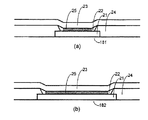
図5は、図3および図4に示した、OELD18の発光面積を変化させることで階調表示を実現するTFT-OELDの、断面図である。図5(a)は、OELD(下位ビット)181の断面図で、図5(b)は、OELD(上位ビット)182の断面図である。OELD(下位ビット)181の発光部25
と、OELD(上位ビット)182の発光部25との比は、1:2になることが望まれている。
【0007】
発光層22は、高分子系のOELDであり、液相プロセスにて形成される。バンク24の表面は、撥液性になっており、発光層22は残らないので、OELD18はパターニングされ、その面積が決定される。バンク24の側面については、撥液性になるか親液性になるか
は、材料・プロセスに依存する。
【0008】
図5では、バンク24の側面が、親液性の場合を仮定している。液相プロセス特有の現象として、発光層22が、バンク24の側面に引き寄せられたような断面形状となっている。この場合、発光層22のより薄い部分を電流は流れ、この部分が発光部25となる。ここで述べたような、発光層22の断面形状は、液体の量・液体の物性・液体の初期位置・基板の状態・温度・雰囲気などに敏感で、制御するのは困難である。すなわち、望みどおりの発光面積の絶対値を得ることは、難しい。このため、OELD(下位ビット)181の発光部25と、OELD(上位ビット)182の発光部25との比を、正確に1:2にすることは困難で、結局、正確な階調を得ることは、難しい。
【0009】
図6は、図5と同様、OELD(下位ビット)181の断面図(図6(a))およびOELD(上位ビット)182の断面図(図5(b))である。図6では、バンク24の側面が、撥液性の場合を仮定している。液相プロセス特有の現象として、発光層22が、バンク24の側面から遠ざかるよ
うな断面形状となっている。この場合も、発光層22のより薄い部分を電流は流れ、この部分が発光部25となる。このときも、図5の場合と同様に、OELD(下位ビット)181の発光部25と、OELD(上位ビット)182の発光部25との比を、正確に1:2にすることは困難
で、正確な階調を得ることは、難しい。
【0010】
そこで、本発明の目的は、正確な発光部25の比を得て、正確な階調を得ることである。
【0011】
【課題を解決するための手段】
(1) 請求項1記載の本発明は、各画素に、複数のTFTおよび複数のOELDが形成され、TFTおよびOELDは、直列に接続され、TFTのオン・オフ状態を切り替え、OELDを発光させる面積を制御することで、階調を実現する、表示装置において、複数のOELD
は、各々同じ形状であり、OELDを発光させる個数を制御することで、階調を実現することを特徴とする、表示装置である。
【0012】
本構成によれば、OELDが、液相プロセス特有の現象として、バンクの側面に引き寄せられたような断面形状あるいはバンクの側面から遠ざかるような断面形状となった場合でも、各OELDの発光部を同一な面積とし、正確な階調を得ることが、可能となる。
何故なら、本構成でも、望みどおりの発光面積の絶対値を得ることは、難しいが、複数のOELDの発光面積は互いに等しくなるため、これらの個数を制御することで、発光面積の比を正確にすることが可能だからである。
【0013】
(2) 請求項2記載の本発明は、請求項1記載の、表示装置において、複数のOELDは、円形であることを特徴とする、表示装置である。
【0014】
本構成によれば、より正確に各OELDの発光部を同一な面積とし、正確な階調を得ることが、可能となる。その理由は、次のとおりである。OELDが矩形等の頂点を持っている形状の場合には、その頂点部の引き寄せられる、あるいは、頂点部が満たされな
いなどの現象が発生する可能性がある。この現象は、上記した断面形状の問題と同じ理由で、正確な階調を得るための妨げになる。この現象は、上記した断面形状の問題よりも、さらに液体の量・液体の物性・液体の初期位置・基板の状態・温度・雰囲気などに敏感で、隣接するOELD間でも制御するのは困難である。OELDを円形にすることで、この現象を回避できる。
【0015】
(3) 請求項3記載の本発明は、請求項1記載の、表示装置において、複数のOELDは、横方向あるいは縦方向に、等間隔に配置されていることを特徴とする、表示装置である。
【0016】
本構成によれば、より正確に各OELDの発光部を同一な面積とし、正確な階調を得ることが、可能となる。その理由は、次のとおりである。スピンコート・ブレード塗りでOELDを形成するときは、一旦画素全体に塗布された発光層が、バンク表面の撥液性のために、自然とバンクの凹部に流れ込む。インクジェットのよる場合も、ときにはこのようになる。このとき、バンク凹部の周囲の凸部の面積が広いところでは、この部分に塗布された発光層が、すべてバンク凹部に流れ込むため、発光層は厚くなる。バンク凹部の周囲の凸部の面積が狭いところでは、発光層は薄くなる。結局、発光層の膜厚のバラツキが発生する。複数のOELDを、横方向あるいは縦方向に、等間隔に配置することで、このバラツキを回避できる。
【0017】
また、本構成によれば、インクジェットプロセスによりOELDを形成する場合に、等間隔でインク吐出すればよいため、製造が簡単となる可能性がある。
【0018】
【発明の実施の形態】
以下、本発明の好ましい実施の形態を、図面に基づいて説明する。
【0019】
(実施例1)
図7は、本発明の実施例1に係るTFT-OELDの、画素を示す図である。ここでは、ひとつの画素11のみ図記しているが、実際には複数行・複数列の多数の画素11が存在する。
【0020】
OELD(下位ビット)181は、OELD(下位ビット・矩形)1811から成り、OELD(上位ビット)182は、OELD(上位ビット・第1・矩形)18211とOELD(上位ビット・第2・矩形)18221から成っている。請求項1で示したように、OELD(下位ビット・矩形)1811・OELD(上位ビット・第1・矩形)18211・OELD(上位ビット・第2・矩形)18221は同じ形状をしているので、同じ発光面積が得られ、発光するOELD18の個数を変化させることで、正確な階調を得ることが可能となる。
【0021】
(実施例2)
図8は、本発明の実施例2に係るTFT-OELDの、画素を示す図である。ここでは、ひとつの画素11のみ図記しているが、実際には複数行・複数列の多数の画素11が存在する。
【0022】
OELD(下位ビット)181は、OELD(下位ビット・円形)1812から成り、OELD(上位ビット)182は、OELD(上位ビット・第1・円形)18212とOELD(上位ビット・第2・円形)18222から成っている。請求項2で示したように、OELD(下位ビット・円形)1812・OELD(上位ビット・第1・円形)18212・OELD(上位ビット・第2・円形)18222は、円形となっているので、より正確に同じ発光面積が得られ、正確な階調を得ることが可能となる。
【0023】
(実施例3)
図9は、本発明の実施例3に係るTFT-OELDの、画素を示す図である。ここでは、ひとつの画素11のみ図記しているが、実際には複数行・複数列の多数の画素11が存在する。
【0024】
OELD(下位ビット)181は、OELD(下位ビット・円形)1812から成り、OELD(上位ビット)182は、OELD(上位ビット・第1・円形)18212とOELD(上位ビット・第2・円形)18222から成っている。請求項3で示したように、OELD(下位ビット・円形)1812・OELD(上位ビット・第1・円形)18212・OELD(上位ビット・第2・円形)18222は、その画素11の内部だけでなく、隣接する画素11に対しても、横方向および縦方向に、等間隔に配置されている。このため、より正確に各OELDの発光部を同一な面積とし、正確な階調を得ることが、可能となる。
【0025】
なお、各画素に形成されるEL素子として、実施例1では、矩形状の素子を例として示し、実施例2,3では、円形状の素子を示したが、本発明は、これらに限定されるものではなく、多角形状や楕円形状の素子でも正確な階調を得る事ができる。特に、楕円形状の素子は、円形状の場合と同様に、矩形状としたときの頂点部がないので、頂点部が発光層により満たされないという問題は一切ない。
【発明の効果】
以上述べたように、本発明によればエレクトロルミネッセンス素子の発光させる発光部面積を制御することにより、正確な階調を実現することができる。
【図面の簡単な説明】
【図1】従来の、TFTのコンダクタンスを変化させることで階調表示を実現するTFT-OELDの、画素を示す図。
【図2】 TFT-OELDの、断面図。
【図3】従来の、OELDの発光面積を変化させることで階調表示を実現するTFT-OELDの、画素を示す図。
【図4】従来の、OELDの発光面積を変化させることで階調表示を実現するTFT-OELDの、駆動方法を示す図。
【図5】従来の、OELDの発光面積を変化させることで階調表示を実現するTFT-OELDにおける、OELDの断面図(バンク側面が親液性の場合)。(a)はOELD(下位ビット)の図、(b)はOELD(上位ビット)の図。
【図6】従来の、OELDの発光面積を変化させることで階調表示を実現するTFT-OELDにおける、OELDの断面図(バンク側面が撥液性の場合)。(a)はOELD(下位ビット)の図、(b)はOELD(上位ビット)の図。
【図7】本発明の実施例1に係るTFT-OELDの画素を示す図。
【図8】本発明の実施例2に係るTFT-OELDの画素を示す図。
【図9】本発明の実施例3に係るTFT-OELDの画素を示す図。
【符号の説明】
11 画素
12 走査線
13 信号線
131 信号線(下位ビット)
132 信号線(上位ビット)
14 電流供給線
15 保持容量
151 保持容量(下位ビット)
152 保持容量(上位ビット)
16 サンプリングTFT
161 サンプリングTFT(下位ビット)
162 サンプリングTFT(上位ビット)
17 ドライビングTFT
171 ドライビングTFT(下位ビット)
172 ドライビングTFT(上位ビット)
18 OELD
181 OELD(下位ビット)
1811 OELD(下位ビット・矩形)
1812 OELD(下位ビット・円形)
182 OELD(上位ビット)
18211 OELD(上位ビット・第1・矩形)
18221 OELD(上位ビット・第2・矩形)
18212 OELD(上位ビット・第1・円形)
18222 OELD(上位ビット・第2・円形)
21 陽極
22 発光層
23 陰極
24 バンク
25 発光部
31 走査電位
321 信号電位(下位ビット)
322 信号電位(上位ビット)
Claims (6)
- 複数の画素を有し、各画素に複数の薄膜トランジスタ及び複数の有機エレクトロルミネッセンス素子を備える表示装置であって、
前記各有機エレクトロルミネッセンス素子は各々同じ形状であり、
前記各薄膜トランジスタはオン状態あるいはオフ状態のいずれかをとり、
前記各薄膜トランジスタのオン・オフ状態を切り替えることで前記複数の有機エレクトロルミネッセンス素子の発光する個数を制御して階調表示すること
を特徴とする表示装置。 - 請求項1に記載の表示装置において、
前記複数の有機エレクトロルミネッセンス素子は円形であること
を特徴とする表示装置。 - 請求項1または請求項2に記載の表示装置において、
前記複数の有機エレクトロルミネッセンス素子は横方向に等間隔に配置されていること
を特徴とする表示装置。 - 請求項1乃至請求項3のいずれかに記載の表示装置において、
前記複数の有機エレクトロルミネッセンス素子は縦方向に等間隔に配置されていること
を特徴とする表示装置。 - 請求項1に記載の表示装置において、
少なくとも第1、第2の信号線をさらに備え、
前記各画素は、
さらに、前記第1の信号線に接続された第1のサンプリング薄膜トランジスタ、及び前記第2の信号線に接続された第2のサンプリング薄膜トランジスタを含み、
前記複数の有機エレクトロルミネッセンス素子のうち、1個の有機エレクトロルミネッセンス素子が前記第1のサンプリング薄膜トランジスタを介して前記第1の信号線から供給される信号で発光が制御されるとともに、前記1個の有機エレクトロルミネッセンス素子以外の2個の有機エレクトロルミネッセンス素子が前記第2のサンプリング薄膜トランジスタを介して前記第2の信号線から供給される信号で発光が制御されること
を特徴とする表示装置。 - 請求項5に記載の表示装置において、
複数の走査線をさらに備え、
前記第1のサンプリング薄膜トランジスタのゲート及び前記第2のサンプリング薄膜トランジスタのゲートが前記複数の走査線のうちの共通の1つの走査線に接続されていること
を特徴とする表示装置。
Priority Applications (12)
| Application Number | Priority Date | Filing Date | Title |
|---|---|---|---|
| JP30144899A JP4092827B2 (ja) | 1999-01-29 | 1999-10-22 | 表示装置 |
| KR1019990055506A KR100664450B1 (ko) | 1998-12-07 | 1999-12-07 | 이미지-처리 장치 및 이미지-처리 방법 |
| US09/468,356 US6225750B1 (en) | 1999-01-29 | 1999-12-21 | Display device |
| TW088123045A TW507185B (en) | 1999-01-29 | 1999-12-27 | Organic electroluminescent display device |
| DE60004574T DE60004574T2 (de) | 1999-01-29 | 2000-01-18 | Organische elektrolumineszierende Anzeigevorrichtung |
| EP00300329A EP1024472B1 (en) | 1999-01-29 | 2000-01-18 | Organic electroluminescent display device |
| EP02079261A EP1288903A3 (en) | 1999-01-29 | 2000-01-18 | Organic electroluminescent display device |
| KR10-2000-0003881A KR100467905B1 (ko) | 1999-01-29 | 2000-01-27 | 표시 장치 |
| CN00101923A CN1123799C (zh) | 1999-01-29 | 2000-01-28 | 显示装置 |
| US09/820,763 US6388389B2 (en) | 1999-01-29 | 2001-03-30 | Display device |
| US10/112,710 US6469450B2 (en) | 1999-01-29 | 2002-04-02 | Display device |
| US10/233,402 US6642665B2 (en) | 1999-01-29 | 2002-09-04 | Display device |
Applications Claiming Priority (3)
| Application Number | Priority Date | Filing Date | Title |
|---|---|---|---|
| JP11-21623 | 1999-01-29 | ||
| JP2162399 | 1999-01-29 | ||
| JP30144899A JP4092827B2 (ja) | 1999-01-29 | 1999-10-22 | 表示装置 |
Publications (3)
| Publication Number | Publication Date |
|---|---|
| JP2000284727A JP2000284727A (ja) | 2000-10-13 |
| JP2000284727A5 JP2000284727A5 (ja) | 2005-02-10 |
| JP4092827B2 true JP4092827B2 (ja) | 2008-05-28 |
Family
ID=26358710
Family Applications (1)
| Application Number | Title | Priority Date | Filing Date |
|---|---|---|---|
| JP30144899A Expired - Lifetime JP4092827B2 (ja) | 1998-12-07 | 1999-10-22 | 表示装置 |
Country Status (7)
| Country | Link |
|---|---|
| US (4) | US6225750B1 (ja) |
| EP (2) | EP1024472B1 (ja) |
| JP (1) | JP4092827B2 (ja) |
| KR (2) | KR100664450B1 (ja) |
| CN (1) | CN1123799C (ja) |
| DE (1) | DE60004574T2 (ja) |
| TW (1) | TW507185B (ja) |
Families Citing this family (65)
| Publication number | Priority date | Publication date | Assignee | Title |
|---|---|---|---|---|
| FR2772501B1 (fr) * | 1997-12-15 | 2000-01-21 | Thomson Lcd | Dispositif de commande matriciel |
| JP2000031880A (ja) * | 1998-07-16 | 2000-01-28 | Kokusai Electric Co Ltd | 無線中継装置 |
| JP4092827B2 (ja) * | 1999-01-29 | 2008-05-28 | セイコーエプソン株式会社 | 表示装置 |
| US6366025B1 (en) * | 1999-02-26 | 2002-04-02 | Sanyo Electric Co., Ltd. | Electroluminescence display apparatus |
| WO2001073738A1 (fr) * | 2000-03-30 | 2001-10-04 | Seiko Epson Corporation | Afficheur |
| TW521237B (en) * | 2000-04-18 | 2003-02-21 | Semiconductor Energy Lab | Light emitting device |
| JP2001305998A (ja) | 2000-04-25 | 2001-11-02 | Alpine Electronics Inc | 表示装置 |
| US7315295B2 (en) * | 2000-09-29 | 2008-01-01 | Seiko Epson Corporation | Driving method for electro-optical device, electro-optical device, and electronic apparatus |
| TW522577B (en) | 2000-11-10 | 2003-03-01 | Semiconductor Energy Lab | Light emitting device |
| JP4632337B2 (ja) * | 2000-11-10 | 2011-02-16 | 株式会社半導体エネルギー研究所 | 発光装置 |
| US7071911B2 (en) * | 2000-12-21 | 2006-07-04 | Semiconductor Energy Laboratory Co., Ltd. | Light emitting device, driving method thereof and electric equipment using the light emitting device |
| JP4072332B2 (ja) * | 2001-01-09 | 2008-04-09 | シャープ株式会社 | 液晶表示装置およびその駆動方法 |
| JP3989718B2 (ja) * | 2001-01-18 | 2007-10-10 | シャープ株式会社 | メモリ一体型表示素子 |
| JP4051936B2 (ja) * | 2001-01-22 | 2008-02-27 | セイコーエプソン株式会社 | 電気光学装置及び電子機器 |
| JP4777380B2 (ja) * | 2001-02-07 | 2011-09-21 | 株式会社半導体エネルギー研究所 | 発光装置 |
| JP4822590B2 (ja) * | 2001-02-08 | 2011-11-24 | 三洋電機株式会社 | 有機el回路 |
| KR100407768B1 (ko) * | 2001-07-06 | 2003-12-03 | 주식회사 대한전광 | 유기전계발광소자를 이용한 전광판용 디스플레이 픽셀 및모듈 |
| US7483001B2 (en) * | 2001-11-21 | 2009-01-27 | Seiko Epson Corporation | Active matrix substrate, electro-optical device, and electronic device |
| JP3698208B2 (ja) * | 2001-12-06 | 2005-09-21 | セイコーエプソン株式会社 | 電気光学装置及び電子機器 |
| US6810919B2 (en) * | 2002-01-11 | 2004-11-02 | Seiko Epson Corporation | Manufacturing method for display device, display device, manufacturing method for electronic apparatus, and electronic apparatus |
| US20050180083A1 (en) | 2002-04-26 | 2005-08-18 | Toshiba Matsushita Display Technology Co., Ltd. | Drive circuit for el display panel |
| KR100435054B1 (ko) * | 2002-05-03 | 2004-06-07 | 엘지.필립스 엘시디 주식회사 | 유기전계 발광소자와 그 제조방법 |
| KR20030086166A (ko) * | 2002-05-03 | 2003-11-07 | 엘지.필립스 엘시디 주식회사 | 유기전계 발광소자와 그 제조방법 |
| US20040035360A1 (en) * | 2002-05-17 | 2004-02-26 | Semiconductor Energy Laboratory Co., Ltd. | Manufacturing apparatus |
| JP4459521B2 (ja) * | 2002-10-17 | 2010-04-28 | 大日本印刷株式会社 | エレクトロルミネッセンス表示装置 |
| WO2004049286A1 (ja) * | 2002-11-25 | 2004-06-10 | Toshiba Matsushita Display Technology Co., Ltd. | 有機el表示パネル |
| KR101255532B1 (ko) * | 2002-12-27 | 2013-04-24 | 가부시키가이샤 한도오따이 에네루기 켄큐쇼 | 표시 장치 |
| JP2004220021A (ja) * | 2002-12-27 | 2004-08-05 | Semiconductor Energy Lab Co Ltd | 表示装置 |
| JP4619289B2 (ja) | 2003-03-26 | 2011-01-26 | 株式会社半導体エネルギー研究所 | 表示装置及びその駆動方法、並びに電子機器 |
| KR101115291B1 (ko) * | 2003-04-25 | 2012-03-05 | 가부시키가이샤 한도오따이 에네루기 켄큐쇼 | 액적 토출 장치, 패턴의 형성 방법, 및 반도체 장치의 제조 방법 |
| US6771028B1 (en) * | 2003-04-30 | 2004-08-03 | Eastman Kodak Company | Drive circuitry for four-color organic light-emitting device |
| US20040257352A1 (en) * | 2003-06-18 | 2004-12-23 | Nuelight Corporation | Method and apparatus for controlling |
| CN100533808C (zh) * | 2004-01-26 | 2009-08-26 | 株式会社半导体能源研究所 | 显示器件及其制造方法以及电视设备 |
| TWI366701B (en) * | 2004-01-26 | 2012-06-21 | Semiconductor Energy Lab | Method of manufacturing display and television |
| US20050200294A1 (en) * | 2004-02-24 | 2005-09-15 | Naugler W. E.Jr. | Sidelight illuminated flat panel display and touch panel input device |
| US20050200292A1 (en) * | 2004-02-24 | 2005-09-15 | Naugler W. E.Jr. | Emissive display device having sensing for luminance stabilization and user light or touch screen input |
| JP4466115B2 (ja) * | 2004-02-24 | 2010-05-26 | セイコーエプソン株式会社 | 有機エレクトロルミネッセンス装置、有機エレクトロルミネッセンス装置の製造方法、及び電子機器 |
| US20050200296A1 (en) * | 2004-02-24 | 2005-09-15 | Naugler W. E.Jr. | Method and device for flat panel emissive display using shielded or partially shielded sensors to detect user screen inputs |
| US20060007248A1 (en) * | 2004-06-29 | 2006-01-12 | Damoder Reddy | Feedback control system and method for operating a high-performance stabilized active-matrix emissive display |
| FR2866973B1 (fr) * | 2004-02-27 | 2006-08-04 | Commissariat Energie Atomique | Dispositif ameliore d'adressage de pixels |
| US7462514B2 (en) | 2004-03-03 | 2008-12-09 | Semiconductor Energy Laboratory Co., Ltd. | Semiconductor device and method for manufacturing the same, liquid crystal television, and EL television |
| US7642038B2 (en) | 2004-03-24 | 2010-01-05 | Semiconductor Energy Laboratory Co., Ltd. | Method for forming pattern, thin film transistor, display device, method for manufacturing thereof, and television apparatus |
| US20050243023A1 (en) * | 2004-04-06 | 2005-11-03 | Damoder Reddy | Color filter integrated with sensor array for flat panel display |
| CN1981318A (zh) * | 2004-04-12 | 2007-06-13 | 彩光公司 | 用于有源矩阵发光显示器的低功耗电路及其控制方法 |
| US20050248515A1 (en) * | 2004-04-28 | 2005-11-10 | Naugler W E Jr | Stabilized active matrix emissive display |
| KR101043394B1 (ko) * | 2004-05-14 | 2011-06-22 | 삼성전자주식회사 | 화성형성장치 및 방법 |
| US8158517B2 (en) * | 2004-06-28 | 2012-04-17 | Semiconductor Energy Laboratory Co., Ltd. | Method for manufacturing wiring substrate, thin film transistor, display device and television device |
| JP2006065284A (ja) | 2004-07-26 | 2006-03-09 | Seiko Epson Corp | 発光装置及び電子機器 |
| CN101251986B (zh) * | 2004-07-26 | 2012-01-04 | 精工爱普生株式会社 | 发光装置 |
| KR100699997B1 (ko) * | 2004-09-21 | 2007-03-26 | 삼성에스디아이 주식회사 | 다수개의 구동 트랜지스터와 다수개의 애노드 또는캐소드전극을 갖는 유기 전계 발광 표시장치 |
| US20070001954A1 (en) * | 2005-07-04 | 2007-01-04 | Semiconductor Energy Laboratory Co., Ltd. | Display device and driving method of display device |
| KR100729077B1 (ko) * | 2005-11-14 | 2007-06-14 | 삼성에스디아이 주식회사 | 유기 발광 표시장치 |
| KR100688971B1 (ko) * | 2006-02-16 | 2007-03-08 | 삼성전자주식회사 | 디스플레이장치 |
| KR101304837B1 (ko) * | 2006-12-29 | 2013-09-05 | 엘지전자 주식회사 | 냉장고의 절전형 디스플레이 시스템 |
| JP2008180802A (ja) * | 2007-01-23 | 2008-08-07 | Eastman Kodak Co | アクティブマトリクス型表示装置 |
| JP5242076B2 (ja) * | 2007-04-13 | 2013-07-24 | グローバル・オーエルイーディー・テクノロジー・リミテッド・ライアビリティ・カンパニー | アクティブマトリクス型表示装置 |
| US8130177B2 (en) * | 2008-03-13 | 2012-03-06 | Panasonic Corporation | Organic EL display panel and manufacturing method thereof |
| TWI411992B (zh) * | 2010-12-14 | 2013-10-11 | Au Optronics Corp | 顯示裝置的驅動方法以及顯示裝置 |
| CN103489401B (zh) * | 2013-09-03 | 2016-11-23 | 京东方科技集团股份有限公司 | 像素电路及其驱动方法、阵列基板和显示装置 |
| US9806098B2 (en) | 2013-12-10 | 2017-10-31 | Semiconductor Energy Laboratory Co., Ltd. | Light-emitting device |
| JP2016042195A (ja) * | 2015-11-12 | 2016-03-31 | 株式会社半導体エネルギー研究所 | 表示装置 |
| KR102490894B1 (ko) | 2018-02-08 | 2023-01-25 | 삼성디스플레이 주식회사 | 유기 발광 표시 장치 |
| CN110021260B (zh) * | 2018-06-27 | 2021-01-26 | 京东方科技集团股份有限公司 | 一种像素电路及其驱动方法、显示装置 |
| CN111769143B (zh) * | 2020-06-23 | 2022-09-09 | 武汉华星光电半导体显示技术有限公司 | 显示面板及其制造方法 |
| US20230011754A1 (en) * | 2021-07-01 | 2023-01-12 | Universal Display Corporation | Means to Reduce OLED Transient Response |
Family Cites Families (12)
| Publication number | Priority date | Publication date | Assignee | Title |
|---|---|---|---|---|
| JPS5688193A (en) * | 1979-12-19 | 1981-07-17 | Citizen Watch Co Ltd | Display unit |
| JPS6122326A (ja) * | 1984-03-23 | 1986-01-30 | Citizen Watch Co Ltd | 階調表示装置 |
| US5459678A (en) * | 1992-07-02 | 1995-10-17 | Feasey; Michael F. | Method and calibration apparatus for calibrating computer monitors used in the printing and textile industries |
| US5714968A (en) * | 1994-08-09 | 1998-02-03 | Nec Corporation | Current-dependent light-emitting element drive circuit for use in active matrix display device |
| US5732151A (en) * | 1995-03-03 | 1998-03-24 | Hewlett-Packard Company | Computerized memory mapping method for transforming color data |
| US5585695A (en) * | 1995-06-02 | 1996-12-17 | Adrian Kitai | Thin film electroluminescent display module |
| US5834894A (en) * | 1995-09-14 | 1998-11-10 | Casio Computer Co., Ltd. | Carrier injection type organic electro-luminescent device which emits light in response to an application of a voltage |
| EP0812526B1 (en) * | 1995-12-30 | 2001-08-08 | Casio Computer Co., Ltd. | Display device for performing display operation in accordance with signal light and driving method therefor |
| DE69825402T2 (de) * | 1997-03-12 | 2005-08-04 | Seiko Epson Corp. | Pixelschaltung, anzeigevorrichtung und elektronische apparatur mit stromgesteuerter lichtemittierender vorrichtung |
| JPH1173158A (ja) * | 1997-08-28 | 1999-03-16 | Seiko Epson Corp | 表示素子 |
| JP2000058270A (ja) * | 1998-08-04 | 2000-02-25 | Sony Corp | 光学素子および有機elディスプレイ |
| JP4092827B2 (ja) * | 1999-01-29 | 2008-05-28 | セイコーエプソン株式会社 | 表示装置 |
-
1999
- 1999-10-22 JP JP30144899A patent/JP4092827B2/ja not_active Expired - Lifetime
- 1999-12-07 KR KR1019990055506A patent/KR100664450B1/ko not_active IP Right Cessation
- 1999-12-21 US US09/468,356 patent/US6225750B1/en not_active Expired - Lifetime
- 1999-12-27 TW TW088123045A patent/TW507185B/zh not_active IP Right Cessation
-
2000
- 2000-01-18 EP EP00300329A patent/EP1024472B1/en not_active Expired - Lifetime
- 2000-01-18 EP EP02079261A patent/EP1288903A3/en not_active Withdrawn
- 2000-01-18 DE DE60004574T patent/DE60004574T2/de not_active Expired - Lifetime
- 2000-01-27 KR KR10-2000-0003881A patent/KR100467905B1/ko active IP Right Grant
- 2000-01-28 CN CN00101923A patent/CN1123799C/zh not_active Expired - Lifetime
-
2001
- 2001-03-30 US US09/820,763 patent/US6388389B2/en not_active Expired - Lifetime
-
2002
- 2002-04-02 US US10/112,710 patent/US6469450B2/en not_active Expired - Lifetime
- 2002-09-04 US US10/233,402 patent/US6642665B2/en not_active Expired - Lifetime
Also Published As
| Publication number | Publication date |
|---|---|
| KR20000052429A (ko) | 2000-08-25 |
| US6388389B2 (en) | 2002-05-14 |
| KR100664450B1 (ko) | 2007-01-04 |
| US20020105280A1 (en) | 2002-08-08 |
| US20020011793A1 (en) | 2002-01-31 |
| EP1024472A2 (en) | 2000-08-02 |
| EP1288903A2 (en) | 2003-03-05 |
| EP1024472A3 (en) | 2000-11-15 |
| KR100467905B1 (ko) | 2005-01-24 |
| US6642665B2 (en) | 2003-11-04 |
| JP2000284727A (ja) | 2000-10-13 |
| EP1024472B1 (en) | 2003-08-20 |
| TW507185B (en) | 2002-10-21 |
| DE60004574T2 (de) | 2004-02-26 |
| US6225750B1 (en) | 2001-05-01 |
| CN1123799C (zh) | 2003-10-08 |
| EP1288903A3 (en) | 2003-06-25 |
| US6469450B2 (en) | 2002-10-22 |
| KR20000053629A (ko) | 2000-08-25 |
| DE60004574D1 (de) | 2003-09-25 |
| US20020195969A1 (en) | 2002-12-26 |
| CN1263279A (zh) | 2000-08-16 |
Similar Documents
| Publication | Publication Date | Title |
|---|---|---|
| JP4092827B2 (ja) | 表示装置 | |
| EP2011153B1 (en) | Optoelectronic display and method of manufacturing the same | |
| KR100743948B1 (ko) | 유기 el 장치 및 광학 장치 | |
| US6734505B2 (en) | Thin film transistor and use of same | |
| US7265737B2 (en) | Flat panel display with thin film transistor (TFT) | |
| US20070001592A1 (en) | Method of manufacturing organic EL device, and organic EL device | |
| JP2009071176A (ja) | 表示装置及び表示装置の製造方法 | |
| KR100686343B1 (ko) | 유기 전계 발광 표시 장치 | |
| JP4770557B2 (ja) | 発光素子およびその製造方法、発光装置 | |
| KR100746163B1 (ko) | 디스플레이장치 및 그 제조방법 | |
| JP4483264B2 (ja) | 表示装置及び電子機器 | |
| JP2007514271A (ja) | エレクトロルミネッセンス装置 | |
| KR101294843B1 (ko) | 전계발광소자 및 그 제조방법 | |
| KR100669316B1 (ko) | 유기 전계 발광 표시 장치 | |
| KR100873066B1 (ko) | 유기 전계 발광 장치 및 그 제조방법 | |
| KR20040061988A (ko) | 하이브리드 구조 유기전계발광 소자 및 그의 제조방법 |
Legal Events
| Date | Code | Title | Description |
|---|---|---|---|
| A521 | Request for written amendment filed |
Free format text: JAPANESE INTERMEDIATE CODE: A523 Effective date: 20040304 |
|
| A621 | Written request for application examination |
Free format text: JAPANESE INTERMEDIATE CODE: A621 Effective date: 20040304 |
|
| A977 | Report on retrieval |
Free format text: JAPANESE INTERMEDIATE CODE: A971007 Effective date: 20050826 |
|
| A131 | Notification of reasons for refusal |
Free format text: JAPANESE INTERMEDIATE CODE: A131 Effective date: 20050906 |
|
| A521 | Request for written amendment filed |
Free format text: JAPANESE INTERMEDIATE CODE: A523 Effective date: 20051104 |
|
| A131 | Notification of reasons for refusal |
Free format text: JAPANESE INTERMEDIATE CODE: A131 Effective date: 20071120 |
|
| A521 | Request for written amendment filed |
Free format text: JAPANESE INTERMEDIATE CODE: A523 Effective date: 20080117 |
|
| TRDD | Decision of grant or rejection written | ||
| A01 | Written decision to grant a patent or to grant a registration (utility model) |
Free format text: JAPANESE INTERMEDIATE CODE: A01 Effective date: 20080212 |
|
| A61 | First payment of annual fees (during grant procedure) |
Free format text: JAPANESE INTERMEDIATE CODE: A61 Effective date: 20080225 |
|
| FPAY | Renewal fee payment (event date is renewal date of database) |
Free format text: PAYMENT UNTIL: 20110314 Year of fee payment: 3 |
|
| R150 | Certificate of patent or registration of utility model |
Free format text: JAPANESE INTERMEDIATE CODE: R150 Ref document number: 4092827 Country of ref document: JP Free format text: JAPANESE INTERMEDIATE CODE: R150 |
|
| FPAY | Renewal fee payment (event date is renewal date of database) |
Free format text: PAYMENT UNTIL: 20120314 Year of fee payment: 4 |
|
| FPAY | Renewal fee payment (event date is renewal date of database) |
Free format text: PAYMENT UNTIL: 20120314 Year of fee payment: 4 |
|
| FPAY | Renewal fee payment (event date is renewal date of database) |
Free format text: PAYMENT UNTIL: 20130314 Year of fee payment: 5 |
|
| FPAY | Renewal fee payment (event date is renewal date of database) |
Free format text: PAYMENT UNTIL: 20140314 Year of fee payment: 6 |
|
| S111 | Request for change of ownership or part of ownership |
Free format text: JAPANESE INTERMEDIATE CODE: R313113 |
|
| S111 | Request for change of ownership or part of ownership |
Free format text: JAPANESE INTERMEDIATE CODE: R313113 |
|
| R371 | Transfer withdrawn |
Free format text: JAPANESE INTERMEDIATE CODE: R371 |
|
| S111 | Request for change of ownership or part of ownership |
Free format text: JAPANESE INTERMEDIATE CODE: R313113 |
|
| R350 | Written notification of registration of transfer |
Free format text: JAPANESE INTERMEDIATE CODE: R350 |
|
| R250 | Receipt of annual fees |
Free format text: JAPANESE INTERMEDIATE CODE: R250 |
|
| R250 | Receipt of annual fees |
Free format text: JAPANESE INTERMEDIATE CODE: R250 |
|
| R250 | Receipt of annual fees |
Free format text: JAPANESE INTERMEDIATE CODE: R250 |
|
| R250 | Receipt of annual fees |
Free format text: JAPANESE INTERMEDIATE CODE: R250 |
|
| EXPY | Cancellation because of completion of term |