JP3830238B2 - Active matrix type device - Google Patents
Active matrix type device Download PDFInfo
- Publication number
- JP3830238B2 JP3830238B2 JP23492197A JP23492197A JP3830238B2 JP 3830238 B2 JP3830238 B2 JP 3830238B2 JP 23492197 A JP23492197 A JP 23492197A JP 23492197 A JP23492197 A JP 23492197A JP 3830238 B2 JP3830238 B2 JP 3830238B2
- Authority
- JP
- Japan
- Prior art keywords
- active matrix
- film
- insulating film
- tft
- type device
- Prior art date
- Legal status (The legal status is an assumption and is not a legal conclusion. Google has not performed a legal analysis and makes no representation as to the accuracy of the status listed.)
- Expired - Lifetime
Links
- 239000011159 matrix material Substances 0.000 title claims description 67
- 239000004065 semiconductor Substances 0.000 claims description 44
- 230000001681 protective effect Effects 0.000 claims description 33
- 229910052581 Si3N4 Inorganic materials 0.000 claims description 4
- HQVNEWCFYHHQES-UHFFFAOYSA-N silicon nitride Chemical compound N12[Si]34N5[Si]62N3[Si]51N64 HQVNEWCFYHHQES-UHFFFAOYSA-N 0.000 claims description 4
- 229910010272 inorganic material Inorganic materials 0.000 claims description 2
- 239000011147 inorganic material Substances 0.000 claims description 2
- 239000010408 film Substances 0.000 description 167
- 239000010410 layer Substances 0.000 description 61
- 239000010409 thin film Substances 0.000 description 38
- 229910052782 aluminium Inorganic materials 0.000 description 23
- XAGFODPZIPBFFR-UHFFFAOYSA-N aluminium Chemical compound [Al] XAGFODPZIPBFFR-UHFFFAOYSA-N 0.000 description 23
- 239000000758 substrate Substances 0.000 description 22
- 239000011229 interlayer Substances 0.000 description 18
- 239000003990 capacitor Substances 0.000 description 16
- 238000000034 method Methods 0.000 description 13
- 230000015572 biosynthetic process Effects 0.000 description 11
- QVGXLLKOCUKJST-UHFFFAOYSA-N atomic oxygen Chemical compound [O] QVGXLLKOCUKJST-UHFFFAOYSA-N 0.000 description 8
- 238000002347 injection Methods 0.000 description 8
- 239000007924 injection Substances 0.000 description 8
- 229910052760 oxygen Inorganic materials 0.000 description 8
- 239000001301 oxygen Substances 0.000 description 8
- 230000003071 parasitic effect Effects 0.000 description 8
- 238000004519 manufacturing process Methods 0.000 description 7
- 239000004973 liquid crystal related substance Substances 0.000 description 6
- XUIMIQQOPSSXEZ-UHFFFAOYSA-N Silicon Chemical compound [Si] XUIMIQQOPSSXEZ-UHFFFAOYSA-N 0.000 description 5
- 229910052783 alkali metal Inorganic materials 0.000 description 5
- 150000001340 alkali metals Chemical class 0.000 description 5
- 229910052751 metal Inorganic materials 0.000 description 5
- 239000002184 metal Substances 0.000 description 5
- 239000012466 permeate Substances 0.000 description 5
- 229910052710 silicon Inorganic materials 0.000 description 5
- 239000010703 silicon Substances 0.000 description 5
- BOTDANWDWHJENH-UHFFFAOYSA-N Tetraethyl orthosilicate Chemical compound CCO[Si](OCC)(OCC)OCC BOTDANWDWHJENH-UHFFFAOYSA-N 0.000 description 4
- 238000010586 diagram Methods 0.000 description 4
- 230000000694 effects Effects 0.000 description 4
- 239000007788 liquid Substances 0.000 description 4
- RYGMFSIKBFXOCR-UHFFFAOYSA-N Copper Chemical compound [Cu] RYGMFSIKBFXOCR-UHFFFAOYSA-N 0.000 description 3
- 239000002585 base Substances 0.000 description 3
- 239000010949 copper Substances 0.000 description 3
- 229910052802 copper Inorganic materials 0.000 description 3
- 239000000463 material Substances 0.000 description 3
- 238000005192 partition Methods 0.000 description 3
- 238000005268 plasma chemical vapour deposition Methods 0.000 description 3
- 239000002243 precursor Substances 0.000 description 3
- MYMOFIZGZYHOMD-UHFFFAOYSA-N Dioxygen Chemical compound O=O MYMOFIZGZYHOMD-UHFFFAOYSA-N 0.000 description 2
- WHXSMMKQMYFTQS-UHFFFAOYSA-N Lithium Chemical compound [Li] WHXSMMKQMYFTQS-UHFFFAOYSA-N 0.000 description 2
- VYPSYNLAJGMNEJ-UHFFFAOYSA-N Silicium dioxide Chemical compound O=[Si]=O VYPSYNLAJGMNEJ-UHFFFAOYSA-N 0.000 description 2
- 229910045601 alloy Inorganic materials 0.000 description 2
- 239000000956 alloy Substances 0.000 description 2
- 229910021417 amorphous silicon Inorganic materials 0.000 description 2
- 230000000295 complement effect Effects 0.000 description 2
- 230000007423 decrease Effects 0.000 description 2
- 229910001882 dioxygen Inorganic materials 0.000 description 2
- 238000005401 electroluminescence Methods 0.000 description 2
- 239000007789 gas Substances 0.000 description 2
- 239000011344 liquid material Substances 0.000 description 2
- 229910052744 lithium Inorganic materials 0.000 description 2
- 238000000059 patterning Methods 0.000 description 2
- 230000002093 peripheral effect Effects 0.000 description 2
- 229920000553 poly(phenylenevinylene) Polymers 0.000 description 2
- 229920001721 polyimide Polymers 0.000 description 2
- -1 polyphenylene vinylene Polymers 0.000 description 2
- 239000003870 refractory metal Substances 0.000 description 2
- 239000005871 repellent Substances 0.000 description 2
- 229910052814 silicon oxide Inorganic materials 0.000 description 2
- 238000004544 sputter deposition Methods 0.000 description 2
- OYPRJOBELJOOCE-UHFFFAOYSA-N Calcium Chemical compound [Ca] OYPRJOBELJOOCE-UHFFFAOYSA-N 0.000 description 1
- ZOKXTWBITQBERF-UHFFFAOYSA-N Molybdenum Chemical compound [Mo] ZOKXTWBITQBERF-UHFFFAOYSA-N 0.000 description 1
- RTAQQCXQSZGOHL-UHFFFAOYSA-N Titanium Chemical compound [Ti] RTAQQCXQSZGOHL-UHFFFAOYSA-N 0.000 description 1
- 230000005540 biological transmission Effects 0.000 description 1
- 229910052791 calcium Inorganic materials 0.000 description 1
- 239000011575 calcium Substances 0.000 description 1
- 239000013626 chemical specie Substances 0.000 description 1
- 238000000576 coating method Methods 0.000 description 1
- 238000002425 crystallisation Methods 0.000 description 1
- 230000008025 crystallization Effects 0.000 description 1
- 230000006866 deterioration Effects 0.000 description 1
- 238000009792 diffusion process Methods 0.000 description 1
- 239000012535 impurity Substances 0.000 description 1
- 238000009413 insulation Methods 0.000 description 1
- 238000005224 laser annealing Methods 0.000 description 1
- 150000002739 metals Chemical class 0.000 description 1
- 229910052750 molybdenum Inorganic materials 0.000 description 1
- 239000011733 molybdenum Substances 0.000 description 1
- 150000004767 nitrides Chemical class 0.000 description 1
- 239000011368 organic material Substances 0.000 description 1
- 229910052698 phosphorus Inorganic materials 0.000 description 1
- 239000011574 phosphorus Substances 0.000 description 1
- 229910021420 polycrystalline silicon Inorganic materials 0.000 description 1
- 229920005591 polysilicon Polymers 0.000 description 1
- 239000002994 raw material Substances 0.000 description 1
- 230000002940 repellent Effects 0.000 description 1
- 239000007790 solid phase Substances 0.000 description 1
- 239000002904 solvent Substances 0.000 description 1
- 229910052715 tantalum Inorganic materials 0.000 description 1
- GUVRBAGPIYLISA-UHFFFAOYSA-N tantalum atom Chemical compound [Ta] GUVRBAGPIYLISA-UHFFFAOYSA-N 0.000 description 1
- 229910052719 titanium Inorganic materials 0.000 description 1
- 239000010936 titanium Substances 0.000 description 1
- WFKWXMTUELFFGS-UHFFFAOYSA-N tungsten Chemical compound [W] WFKWXMTUELFFGS-UHFFFAOYSA-N 0.000 description 1
- 229910052721 tungsten Inorganic materials 0.000 description 1
- 239000010937 tungsten Substances 0.000 description 1
- XLYOFNOQVPJJNP-UHFFFAOYSA-N water Substances O XLYOFNOQVPJJNP-UHFFFAOYSA-N 0.000 description 1
Images


Classifications
-
- H—ELECTRICITY
- H05—ELECTRIC TECHNIQUES NOT OTHERWISE PROVIDED FOR
- H05B—ELECTRIC HEATING; ELECTRIC LIGHT SOURCES NOT OTHERWISE PROVIDED FOR; CIRCUIT ARRANGEMENTS FOR ELECTRIC LIGHT SOURCES, IN GENERAL
- H05B33/00—Electroluminescent light sources
- H05B33/12—Light sources with substantially two-dimensional radiating surfaces
- H05B33/26—Light sources with substantially two-dimensional radiating surfaces characterised by the composition or arrangement of the conductive material used as an electrode
-
- H—ELECTRICITY
- H05—ELECTRIC TECHNIQUES NOT OTHERWISE PROVIDED FOR
- H05B—ELECTRIC HEATING; ELECTRIC LIGHT SOURCES NOT OTHERWISE PROVIDED FOR; CIRCUIT ARRANGEMENTS FOR ELECTRIC LIGHT SOURCES, IN GENERAL
- H05B33/00—Electroluminescent light sources
- H05B33/02—Details
- H05B33/04—Sealing arrangements, e.g. against humidity
-
- H—ELECTRICITY
- H01—ELECTRIC ELEMENTS
- H01L—SEMICONDUCTOR DEVICES NOT COVERED BY CLASS H10
- H01L27/00—Devices consisting of a plurality of semiconductor or other solid-state components formed in or on a common substrate
- H01L27/02—Devices consisting of a plurality of semiconductor or other solid-state components formed in or on a common substrate including semiconductor components specially adapted for rectifying, oscillating, amplifying or switching and having at least one potential-jump barrier or surface barrier; including integrated passive circuit elements with at least one potential-jump barrier or surface barrier
- H01L27/12—Devices consisting of a plurality of semiconductor or other solid-state components formed in or on a common substrate including semiconductor components specially adapted for rectifying, oscillating, amplifying or switching and having at least one potential-jump barrier or surface barrier; including integrated passive circuit elements with at least one potential-jump barrier or surface barrier the substrate being other than a semiconductor body, e.g. an insulating body
- H01L27/1214—Devices consisting of a plurality of semiconductor or other solid-state components formed in or on a common substrate including semiconductor components specially adapted for rectifying, oscillating, amplifying or switching and having at least one potential-jump barrier or surface barrier; including integrated passive circuit elements with at least one potential-jump barrier or surface barrier the substrate being other than a semiconductor body, e.g. an insulating body comprising a plurality of TFTs formed on a non-semiconducting substrate, e.g. driving circuits for AMLCDs
- H01L27/1255—Devices consisting of a plurality of semiconductor or other solid-state components formed in or on a common substrate including semiconductor components specially adapted for rectifying, oscillating, amplifying or switching and having at least one potential-jump barrier or surface barrier; including integrated passive circuit elements with at least one potential-jump barrier or surface barrier the substrate being other than a semiconductor body, e.g. an insulating body comprising a plurality of TFTs formed on a non-semiconducting substrate, e.g. driving circuits for AMLCDs integrated with passive devices, e.g. auxiliary capacitors
-
- H—ELECTRICITY
- H05—ELECTRIC TECHNIQUES NOT OTHERWISE PROVIDED FOR
- H05B—ELECTRIC HEATING; ELECTRIC LIGHT SOURCES NOT OTHERWISE PROVIDED FOR; CIRCUIT ARRANGEMENTS FOR ELECTRIC LIGHT SOURCES, IN GENERAL
- H05B33/00—Electroluminescent light sources
- H05B33/12—Light sources with substantially two-dimensional radiating surfaces
- H05B33/22—Light sources with substantially two-dimensional radiating surfaces characterised by the chemical or physical composition or the arrangement of auxiliary dielectric or reflective layers
-
- H—ELECTRICITY
- H10—SEMICONDUCTOR DEVICES; ELECTRIC SOLID-STATE DEVICES NOT OTHERWISE PROVIDED FOR
- H10K—ORGANIC ELECTRIC SOLID-STATE DEVICES
- H10K50/00—Organic light-emitting devices
- H10K50/80—Constructional details
- H10K50/84—Passivation; Containers; Encapsulations
- H10K50/844—Encapsulations
-
- H—ELECTRICITY
- H10—SEMICONDUCTOR DEVICES; ELECTRIC SOLID-STATE DEVICES NOT OTHERWISE PROVIDED FOR
- H10K—ORGANIC ELECTRIC SOLID-STATE DEVICES
- H10K59/00—Integrated devices, or assemblies of multiple devices, comprising at least one organic light-emitting element covered by group H10K50/00
- H10K59/10—OLED displays
- H10K59/12—Active-matrix OLED [AMOLED] displays
- H10K59/122—Pixel-defining structures or layers, e.g. banks
-
- H—ELECTRICITY
- H10—SEMICONDUCTOR DEVICES; ELECTRIC SOLID-STATE DEVICES NOT OTHERWISE PROVIDED FOR
- H10K—ORGANIC ELECTRIC SOLID-STATE DEVICES
- H10K59/00—Integrated devices, or assemblies of multiple devices, comprising at least one organic light-emitting element covered by group H10K50/00
- H10K59/80—Constructional details
- H10K59/87—Passivation; Containers; Encapsulations
- H10K59/873—Encapsulations
-
- H—ELECTRICITY
- H10—SEMICONDUCTOR DEVICES; ELECTRIC SOLID-STATE DEVICES NOT OTHERWISE PROVIDED FOR
- H10K—ORGANIC ELECTRIC SOLID-STATE DEVICES
- H10K50/00—Organic light-emitting devices
- H10K50/80—Constructional details
- H10K50/86—Arrangements for improving contrast, e.g. preventing reflection of ambient light
- H10K50/865—Arrangements for improving contrast, e.g. preventing reflection of ambient light comprising light absorbing layers, e.g. light-blocking layers
Description
【0001】
【発明の属する技術分野】
本発明は、有機半導体膜等の発光薄膜に駆動電流が流れることによって発光するエレクトロルミネッセンス素子(以下、EL素子という。)または発光ダイオード素子(以下、LED素子という。)などの薄膜発光素子を薄膜トランジスタ(以下、TFTという。)で駆動制御するアクティブマトリクス型表示装置に関するものである。
【0002】
【従来の技術】
EL素子またはLED素子などの電流制御型発光素子を用いたアクティブマトリクス型の表示装置が提案されている。このタイプの表示装置に用いられる発光素子はいずれも自己発光するため、液晶表示装置と違ってバックライトを必要とせず、また、視野角依存性が少ないなどの利点もある。
【0003】
図4は、このような電荷注入型の有機半導体薄膜によって発光するEL素子を用いたアクティブマトリクス型表示装置のブロック図である。この図に示すアクティブマトリクス型表示装置1Aでは、透明基板10上に、複数の走査線gateと、該走査線gateの延設方向に対して交差する方向に延設された複数のデータ線sigと、該データ線sigに並列する複数の共通給電線comと、データ線sigと走査線gateとによってマトリクス状に形成された画素7とが構成されている。データ線sigおよび走査線gateに対してはデータ側駆動回路3および走査側駆動回路4が構成されている。各々の画素7には、走査線gateを介して走査信号が供給される導通制御回路50と、この導通制御回路50を介してデータ線sigから供給される画像信号に基づいて発光する薄膜発光素子40とが構成されている。導通制御回路50は、走査線gateを介して走査信号がゲート電極に供給される第1のTFT20と、この第1のTFT20を介してデータ線sigから供給される画像信号を保持する保持容量capと、この保持容量capによって保持された画像信号がゲート電極に供給される第2のTFT30とから構成されている。第2のTFT30と薄膜発光素子40とは、後述する対向電極opと共通給電線comとの間に直列に接続している。この薄膜発光素子40は、第2のTFT30がオン状態になったときには共通給電線comから駆動電流が流れ込んで発光するとともに、この発光状態は保持容量capによって所定の期間、保持される。
【0004】
図5は、図4に示すアクティブマトリクス型表示装置に構成されている画素の1つを抜き出して示す平面図である。図6(A)、(B)、(C)はそれぞれ、図5のA−A′断面図、B−B′断面図、およびC−C′断面図である。
【0005】
このような構成のアクティブマトリクス型表示装置1Aでは、図5および図6(A)、(B)に示すように、いずれの画素7においても、島状の半導体膜を利用して同一工程で第1のTFT20および第2のTFT30が形成されている。第1のTFT20は、ゲート電極21が走査線gateの一部として構成されている。第1のTFT20は、ソース・ドレイン領域の一方に第1の層間絶縁膜51のコンタクホールを介してデータ線sigが電気的に接続し、他方にはドレイン電極22が電気的に接続している。ドレイン電極22は、第2のTFT30の形成領域に向けて延設されており、この延設部分には第2のTFT30のゲート電極31が第1の層間絶縁膜51のコンタクトホールを介して電気的に接続している。第2のTFT30のソース・ドレイン領域の一方には、第1の層間絶縁膜51のコンタクトホールを介して中継電極35が電気的に接続し、この中継電極35には第2の層間絶縁膜52のコンタクトホールを介して薄膜発光素子40の画素電極41が電気的に接続している。
【0006】
画素電極41は、図5および図6(B)、(C)からわかるように各画素7毎に独立して形成されている。画素電極41の上層側には、有機半導体膜43および対向電極opがこの順に積層されている。対向電極opは、少なくとも表示部11を覆うように形成されている。
【0007】
再び、図5および図6(A)において、第2のTFT30のソース・ドレイン領域のもう一方には、第1の層間絶縁膜51のコンタクトホールを介して共通給電線comが電気的に接続している。共通給電線comの延設部分39は、第2のTFT30のゲート電極31の延設部分36に対して、第1の層間絶縁膜51を誘電体膜として挟んで対向し、保持容量capを構成している。
【0008】
【発明が解決しようとする課題】
このようなアクティブマトリクス型表示装置1Aは、透明基板10自体に対向電極opが積層されているので、アクティブマトリクス型液晶表示装置と相違して、対向基板を重ねる必要がないという大きな利点がある。しかし、薄膜発光素子40は薄い対向電極opで覆われているだけなので、対向電極opを拡散、透過して有機半導体膜43に水分や酸素が侵入し、薄膜発光素子40の発光効率の低下、その駆動電圧の上昇(しきい値電圧の高電圧側へのシフト)、信頼性の低下などを発生させるおそれがある。前記水分や酸素の侵入を防止するため、従来のアクティブマトリクス型表示装置1Aでは、その少なくとも表示部11を対向基板で覆い、この対向基板の外周を封止する方法がとられていた。しかし、この方法は前述の液晶表示装置に比しての利点を損なうことになる。
【0009】
そこで、本発明の課題は、簡単な構造で薄膜発光素子を水分等から保護することのできるアクティブマトリクス型表示装置を提供することにある。
【0010】
【課題を解決する手段】
上記課題を解決するため、本発明のアクティブマトリクス型装置は、複数の走査線と、前記複数の走査線を駆動する走査線駆動回路と、前記複数の走査線と交差する複数のデータ線と、前記複数の走査線と前記複数のデータ線との交差に対応して形成された複数のトランジスタと、を含み、前記複数のトランジスタは第1の絶縁膜で覆われ、かつ、前記第1の絶縁膜に設けられた複数のコンタクトホールを介して該第1の絶縁膜上に形成された複数の画素電極に接続され、前記複数の画素電極は電極層と複数の有機半導体膜を挟み、前記第1の絶縁膜上に前記有機半導体膜より厚い第2の絶縁膜が形成され、前記第2の絶縁膜は、前記複数の画素電極の間及び前記走査線駆動回路の上方に位置し、前記電極層は前記第2の絶縁膜上に形成され、前記電極層上には保護膜が形成されてなることを特徴とする。また、前記第2の絶縁膜は前記複数の有機半導体膜の間及び前記複数のトランジスタの上方に位置し、かつ、前記画素電極上に重なって形成されてもよい。また、前記電極層は少なくとも前記複数の画素電極を覆う範囲で前記第1の絶縁膜と重なってもよい。さらに、前記複数のトランジスタは複数の中継電極に接続され、前記複数の中継電極は前記複数の画素電極に接続されてなることを特徴とする。このとき、前記第2の絶縁膜は前記複数の中継電極と重なるよう形成されてもよい。
【0011】
本発明では、例えば対向電極である電極層の上層側には保護膜が形成されているので、電極層を拡散、透過してくる水分等から発光素子等を保護することができる。また、電極層の劣化を抑えることができるため、トランジスタを劣化させる化学種の発生を抑えることができる。さらに、保護膜で発光素子等を保護するので、電極層に用いる材料としては、例えば発光素子の発光効率や駆動電圧などの面からその材質を選択すればよく、発光素子を保護する性能が高いものに限定されないという利点もある。
【0012】
本発明において、前記発光薄膜の周辺の、前記基板と前記対向電極との間には、前記発光薄膜よりも厚い絶縁膜が形成されていることが好ましい。薄膜発光素子を用いたアクティブマトリクス型装置では、対向電極は少なくとも表示部の全面に形成され、データ線と対向する状態にあるため、このままではデータ線に対して大きな容量が寄生することになる。しかるに本発明では、データ線と対向電極との間に厚い絶縁膜を介在させたので、データ線に容量が寄生することを防止できる。その結果、データ側駆動回路の負荷を低減できるので、低消費電力化あるいは表示動作の高速化を図ることができる。また、このような絶縁膜を形成すれば、この絶縁膜で区画された領域内に発光薄膜をインクジェット法により形成する際に、前記絶縁膜を吐出液のはみ出しを防止するバンク層として利用することができる。
【0013】
本発明において、前記対向電極は、たとえばアルカリ金属含有アルミニウム膜から構成され、このような膜で対向電極を構成した場合には、水分などが拡散、透過していく可能性が高いことから、保護膜を形成した効果が顕著である。
【0014】
本発明において、前記保護膜は、シリコン窒化膜などの絶縁膜で構成してもよいが、高融点金属あるいはその合金などの導電膜から構成してもよい。また、前記保護膜を純アルミニウム膜、シリコン含有アルミニウム膜、銅含有アルミニウム膜などの導電膜から構成してもよい。さらには、前記保護膜を導電膜と絶縁膜との2層構造としてもよい。対向電極に積層される保護膜を導電膜で形成した場合には、対向電極の電気的抵抗を低下させたのと同様な効果を得ることができる。また、前記の有機半導体膜の形成領域を区画する厚い絶縁膜を形成した場合にこの絶縁膜が形成する大きな段差によって、その上層側に形成される対向電極に断線が発生させるおそれがあるが、対向電極に積層される保護膜を導電膜で形成した場合には、かかる導電膜によって冗長配線構造が形成されるので、対向電極の断線を防止することができる。それ故、アクティブマトリクス型装置において、有機半導体膜の周りに厚い絶縁膜を形成して寄生容量などを抑えたとしても、絶縁膜の上層に形成する対向電極に断線が発生しないので、アクティブマトリクス型装置の表示品質および信頼性を向上することができる。
【0015】
本発明では、前記導通制御回路は、前記走査信号がゲート電極に供給される第1のTFT、および該第1のTFTを介してゲート電極が前記データ線に接続する第2のTFTを備え、該第2のTFTと前記薄膜発光素子は、前記データ線および走査線とは別に構成された駆動電流供給用の共通給電線と前記対向電極との間に直列に接続していることが好ましい。すなわち、導通制御回路を1つTFTと保持容量で構成することも可能ではあるが、表示品位を高くするという観点からすれば各画素の導通制御回路を2つのTFTと保持容量で構成することが好ましい。
【0016】
【発明の実施の形態】
図面を参照して、本発明の実施の形態を説明する。なお、以下の説明において、図4ないし図6を参照して説明した要素と共通する部分には同一の符号を付してある。
【0017】
(全体構成)
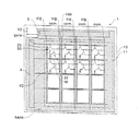
図1は、アクティブマトリクス型表示装置の全体のレイアウトを模式的に示すブロック図である。図2は、それに構成されている画素の1つを抜き出して示す平面図、図3(A)、(B)、(C)はそれぞれ図2のA−A′断面図、B−B′断面図、およびC−C′断面図である。
【0018】
図1に示すアクティブマトリクス型表示装置1では、その基体たる透明基板10の中央部分が表示部11とされている。透明基板10の外周部分のうち、データ線sigの端部には画像信号を出力するデータ側駆動回路3が構成され、走査線gateの端部には走査信号を出力する走査側駆動回路4が構成されている。これらの駆動回路3、4では、N型のTFTとP型のTFTとによって相補型TFTが構成され、この相補型TFTは、シフトレジスタ回路、レベルシフタ回路、アナログスイッチ回路などを構成している。表示部11では、アクティブマトリクス型液晶表示装置のアクティブマトリクス基板と同様、透明基板10上に、複数の走査線gateと、該走査線gateの延設方向に対して交差する方向に延設された複数のデータ線sigとによって、複数の画素7がマトリクス状に構成されている。
【0019】
各々の画素7には、走査線gateを介して走査信号が供給される導通制御回路50と、この導通制御回路50を介してデータ線sigから供給される画像信号に基づいて発光する薄膜発光素子40とが構成されている。ここに示す例においては、導通制御回路50は、走査線gateを介して走査信号がゲート電極に供給される第1のTFT20と、この第1のTFT20を介してデータ線sigから供給される画像信号を保持する保持容量capと、この保持容量capによって保持された画像信号がゲート電極に供給される第2のTFT30とから構成されている。第2のTFT30と薄膜発光素子40とは、詳しくは後述する対向電極opと共通給電線comとの間に直列に接続している。
【0020】
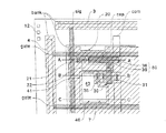
このような構成のアクティブマトリクス型表示装置1では、図2および図3(A)、(B)に示すように、いずれの画素7においても、島状の半導体膜(シリコン膜)を利用して第1のTFT20および第2のTFT30が形成されている。
【0021】
第1のTFT20は、ゲート電極21が走査線gateの一部として構成されている。第1のTFT20は、ソース・ドレイン領域の一方に第1層間絶縁膜51のコンタクホールを介してデータ線sigが電気的に接続し、他方にはドレイン電極22が電気的に接続している。ドレイン電極22は、第2のTFT30の形成領域に向けて延設されており、この延設部分には第2のTFT30のゲート電極31が第1の層間絶縁膜51のコンタクトホールを介して電気的に接続している。
【0022】
第2のTFT30のソース・ドレイン領域の一方には、第1の層間絶縁膜51のコンタクトホールを介して、データ線sigと同時形成された中継電極35が電気的に接続し、この中継電極35には第2の層間絶縁膜52のコンタクトホールを介して薄膜発光素子40のITO膜からなる透明な画素電極41が電気的に接続している。
【0023】
図2および図3(B)、(C)からわかるように、画素電極41は各画素7毎に独立して形成されている。画素電極41の上層側には、ポリフェニレンビニレン(PPV)などからなる有機半導体膜43、およびリチウムなどのアルカリ金属を含有するアルミニウム、カルシウムなどの金属膜からなる対向電極opがこの順に積層され、薄膜発光素子40が構成されている。有機半導体膜43は各画素7に形成されているが、複数の画素7に跨がってストライプ状に形成される場合もある。対向電極opは、表示部11全体と、少なくとも端子12が形成されている部分の周囲を除いた領域に形成されている。
【0024】
なお、薄膜発光素子40としては、正孔注入層を設けて発光効率(正孔注入率)を高めた構造、電子注入層を設けて発光効率(電子注入率)を高めた構造、正孔注入層および電子注入層の双方を形成した構造を採用することもできる。
【0025】
再び、図2および図3(A)において、第2のTFT30のソース・ドレイン領域のもう一方には、第1の層間絶縁膜51のコンタクトホールを介して共通給電線comが電気的に接続している。共通給電線comの延設部分39は、第2のTFT30のゲート電極31の延設部分36に対して、第1の層間絶縁膜51を誘電体膜として挟んで対向し、保持容量capを構成している。
【0026】
このように構成したアクティブマトリクス型表示装置1では、走査信号によって選択されて第1のTFT20がオン状態になると、データ線sigからの画像信号が第1のTFT20を介して第2のTFT30のゲート電極31に印加されるとともに、画像信号が第1のTFT20を介して保持容量capに書き込まれる。その結果、第2のTFT30がオン状態になると、対向電極opおよび画素電極41をそれぞれ負極および正極として電圧が印加され、印加電圧がしきい値電圧を越えた領域で有機半導体膜43に流れる電流(駆動電流)が急激に増大する。従って、発光素子40は、エレクトロルミネッセンス素子あるいはLED素子として発光し、発光素子40の光は、対向電極opに反射されて透明な画素電極41および透明基板10を透過して出射される。このような発光を行うための駆動電流は、対向電極op、有機半導体膜43、画素電極41、第2のTFT30、および共通給電線comから構成される電流経路を流れるため、第2のTFT30がオフ状態になると、流れなくなる。但し、第2のTFT30のゲート電極は、第1のTFT20がオフ状態になっても、保持容量capによって画像信号に相当する電位に保持されるので、第2のTFT30はオン状態のままである。それ故、発光素子40には駆動電流が流れ続け、この画素は点灯状態のままである。この状態は、新たな画像データが保持容量capに書き込まれて、第2のTFT30がオフ状態になるまで維持される。
【0027】
(薄膜発光素子の保護構造)
このように、薄膜発光素子40を用いたアクティブマトリクス型表示装置1は、透明基板10自体に対向電極opが積層されているので、アクティブマトリクス型液晶表示装置と相違して、対向基板を重ねる必要がないという大きな利点がある。しかし、薄膜発光素子40には、薄い対向電極opを拡散、透過して水分や酸素が侵入してくるおそれがある。特に、本形態では、薄膜発光素子40での電子注入効率を高めてその駆動電圧を下げることを目的に、対向電極opとしてリチウムなどのアルカリ金属を含有するアルミニウム膜が用いられ、このアルカリ金属含有アルミニウム膜は、純アルミニウムに比較して水分や酸素を拡散、透過しやすいことが考えられる。すなわち、アルカル金属含有アルミニウム膜は、純アルミニウム膜、シリコン含有アルミニウム膜、銅含有アルミニウム膜に比較して靱性に乏しく、応力がかかったときに破断しやすいので、クラックなどを介して、水分や酸素が侵入するおそれがある。また、アルカリ金属含有アルミニウム膜の破断面は柱状組織を示し、組織間を水分や酸素が拡散、透過しやすいと考えられる。
【0028】
そこで、本形態では、対向電極opの上層に純アルミニウムからなる保護膜60を形成してある。この純アルミニウムからなる保護膜60は、多少の応力では破断しない靱性を有するので、水分や酸素の侵入経路となるクラックが発生しない。また、純アルミニウムは、その破断面において、アルカリ金属含有アルミニウム膜のような柱状組織を示しておらず、組織間を水分や酸素が透過、侵入するおそれもない。それ故、本形態のアクティブマトリクス型表示装置1は、薄膜発光素子40を水分等から保護することができるので、薄膜発光素子40に発光効率の低下、駆動電圧の上昇(しきい値電圧の高電圧側へのシフト)、信頼性の低下などが発生しない。また、このような純アルミニウム膜からなる保護膜60であれば、半導体プロセスを利用して容易に形成できるので、アクティブマトリクス型表示装置1の製造コストを高めることがない。それ故、薄膜発光素子40を用いたアクティブマトリクス型表示装置40の利点である対向基板を被せる必要がないという利点をそのままにして、アクティブマトリクス型表示装置1の信頼性を向上させることができる。
【0029】
また、保護膜60で薄膜発光素子40を保護するので、対向電極opに用いる材料としては、薄膜発光素子40の発光効率や駆動電圧などの面からその材質を選択すればよく、薄膜発光素子40を保護する性能が高いものに限定されないという利点もある。
【0030】
さらに、本形態では、対向電極opに積層される保護膜60を純アルミニウム膜からなる導電膜で形成したので、対向電極opの電気的抵抗を低下させたのと同様な効果を得ることができる。
【0031】
(バンク層の構造)
このように構成したアクティブマトリクス型表示装置1において、本形態では、データ線sigには大きな容量が寄生することを防止するため、図1、図2、および図3(A)、(B)、(C)に示すように、データ線sigおよび走査線gateに沿って、レジスト膜あるいはポリイミド膜からなる厚い絶縁膜(バンク層bank/左下がりの斜線を広いピッチで付した領域)を設け、このバンク層bankの上層側に対向電極opを形成してある。このため、データ線sigと対向電極opとの間には、第2の層間絶縁膜52と厚いバンク層bankが介在しているので、データ線sigに寄生する容量が極めて小さい。それ故、駆動回路3、4の負荷を低減でき、低消費電力化あるいは表示動作の高速化を図ることができる。
【0032】
また、図1に示すように、透明基板10の周辺領域(表示部11の外側領域)にもバンク層bank(形成領域に斜線を付してある。)を形成する。従って、データ側駆動回路3および走査側駆動回路4はいずれも、バンク層bankによって覆われている。対向電極opは少なくとも表示部11に形成され、駆動回路の形成領域に形成される必要はない。しかし、対向電極opは通常、マスクスパッタで形成されるため、合わせ精度が悪く、対向電極opと駆動回路とが重なることがある。このように駆動回路の形成領域に対して対向電極opが重なる状態にあっても、駆動回路の配線層と対向電極opとの間にバンク層bankが介在することになるので、駆動回路3、4に容量が寄生することを防止できる。このため、駆動回路3、4の負荷を低減でき、低消費電力化あるいは表示動作の高速化を図ることができる。
【0033】
さらに、本形態では、画素電極41の形成領域のうち、導通制御回路50の中継電極35と重なる領域にもバンク層bankが形成されている。このため、中継電極35と重なる領域には有機半導体膜43が形成されない。すなわち、画素電極41の形成領域のうち、平坦な部分のみに有機半導体膜43が形成されるので、有機半導体膜43は一定の膜厚で形成され、表示むらを起こさない。また、中継電極35と重なる領域にバンク層bankがないと、この部分でも対向電極opとの間に駆動電流が流れて有機半導体膜43が発光する。しかし、この光は中継電極35と対向電極opとの間に挟まれて外に出射されず、表示に寄与しない。かかる表示に寄与しない部分で流れる駆動電流は、表示という面からみて無効電流といえる。しかるに本形態では、従来ならこのような無効電流が流れるはずの部分にバンク層bankを形成し、そこに駆動電流が流れることを防止するので、共通給電線comに無駄な電流が流れることが防止できる。それ故、共通給電線comの幅はその分、狭くてよい。その結果として、発光面積を増すことができ、輝度、コントラスト比などの表示性能を向上させることができる。
【0034】
ここで、厚いバンク層bankを形成した場合には、図3に示すように、このバンク層bankが形成する大きな段差bbによって、その上層側に形成される対向電極opに断線が発生させるおそれがある。しかるに本形態では、対向電極opに積層される保護膜60を導電膜で形成してあるので、かかる導電膜(保護膜60)によって冗長配線構造が構成されている。従って、厚いバンク層bankを形成して寄生容量などを抑えたとしても、バンク層bankの上層に形成する対向電極opに断線が発生しないので、アクティブマトリクス型表示装置1の表示品質および信頼性を向上することができる。
【0035】
なお、バンク層bankを黒色のレジストによって形成すると、バンク層bankはブラックマトリクスとして機能し、コントラスト比などの表示の品位が向上する。すなわち、本形態に係るアクティブマトリクス型表示装置1では、対向電極opが透明基板10の表面側において画素7の全面に形成されるため、対向電極opでの反射光がコントラスト比を低下させる。しかるに寄生容量を防止する機能を担うバンク層bankを黒色のレジストで構成すると、バンク層bankはブラックマトリクスとしても機能し、対向電極opからの反射光を遮るので、コントラスト比が向上する。
【0036】
(アクティブマトリクス型表示装置の製造方法)
このように形成したバンク層bankは、有機半導体膜43の形成領域を囲むように構成されているので、アクティブマトリクス型表示装置の製造工程では、インクジェットヘッドから吐出した液状の材料(吐出液)から有機半導体膜43を形成する際に吐出液をせき止め、吐出液が側方にはみ出すことを防止する。なお、以下に説明するアクティブマトリクス型表示装置1の製造方法において、透明基板10上に第1のTFT20および第2のTFT30を製造するまでの工程は、液晶アクティブマトリクス型表示装置1のアクティブマトリクス基板を製造する工程と略同様であるため、図3(A)、(B)、(C)を参照してその概略を簡単に説明する。
【0037】
まず、透明基板10に対して、必要に応じて、TEOS(テトラエトキシシラン)や酸素ガスなどを原料ガスとしてプラズマCVD法により厚さが約2000〜5000オングストロームのシリコン酸化膜からなる下地保護膜(図示せず。)を形成した後、下地保護膜の表面にプラズマCVD法により厚さが約300〜700オングストロームのアモルファスのシリコン膜からなる半導体膜を形成する。次にアモルファスのシリコン膜からなる半導体膜に対して、レーザアニールまたは固相成長法などの結晶化工程を行い、半導体膜をポリシリコン膜に結晶化する。
【0038】
次に、半導体膜をパターニングして島状の半導体膜とし、その表面に対して、TEOS(テトラエトキシシラン)や酸素ガスなどを原料ガスとしてプラズマCVD法により厚さが約600〜1500オングストロームのシリコン酸化膜または窒化膜からなるゲート絶縁膜57を形成する。
【0039】
次に、アルミニウム、タンタル、モリブデン、チタン、タングステンなどの金属膜からなる導電膜をスパッタ法により形成した後、パターニングし、ゲート電極21、31、およびゲート電極31の延設部分36を形成する(ゲート電極形成工程)。この工程では走査線gateも形成する。
【0040】
この状態で、高濃度のリンイオンを打ち込んで、ゲート電極21、31に対して自己整合的にソース・ドレイン領域を形成する。なお、不純物が導入されなかった部分がチャネル領域となる。
【0041】
次に、第1の層間絶縁膜51を形成した後、各コンタクトホールを形成し、次に、データ線sig、ドレイン電極22、共通給電線com、共通給電線comの延設部分39、および中継電極35を形成する。その結果、第1のTFT20、第2のTFT30、および保持容量capが形成される。
【0042】
次に、第2の層間絶縁膜52を形成し、この層間絶縁膜には、中継電極35に相当する部分にコンタクトホール形成する。次に、第2の層間絶縁膜52の表面全体にITO膜を形成した後、パターニングし、コンタクトホールを介して第2のTFT30のソース・ドレイン領域に電気的に接続する画素電極41を画素7毎に形成する。
【0043】
次に、第2の層間絶縁膜52の表面側にレジスト層を形成した後、このレジストを走査線gateおよびデータ線sigに沿って残すようにパターニングし、バンク層bankを形成する。このとき、データ線sigに沿って残すレジスト部分は共通給電線comを覆うように幅広とする。その結果、発光素子40の有機半導体膜43を形成すべき領域はバンク層bankに囲まれる。
【0044】
次に、バンク層bankでマトリクス状に区画された領域内にインクジェット法を利用してR、G、Bに対応する各有機半導体膜43を形成していく。それには、バンク層bankの内側領域に対してインクジェットヘッドから、有機半導体膜43を構成するための液状の材料(前駆体)を吐出し、それをバンク層bankの内側領域で定着させて有機半導体膜43を形成する。ここで、バンク層bankはレジストから構成されているため、撥水性である。これに対して、有機半導体膜43の前駆体は親水性の溶媒を用いているため、有機半導体膜43の塗布領域はバンク層bankによって確実に規定され、隣接する画素7にはみ出ることがない。それ故、有機半導体膜43などを所定領域内だけに形成できる。この工程において、インクジェットヘッドから吐出した前駆体は表面張力の影響で約2μmないし約4μmの厚さに盛り上がるため、バンク層bankは約1μmないし約3μmの厚さが必要である。なお、定着した後の有機半導体膜43の厚さは約0.05μmから約0.2μmである。なお、予めバンク層bankからなる隔壁が1μm以上の高さであれば、バンク層bankが撥水性でなくても、バンク層bankは隔壁として十分に機能する。かかる厚いバンク層bankを形成しておけば、インクジェット法に代えて、塗布法で有機半導体膜43を形成する場合でもその形成領域を規定できる。
【0045】
しかる後には、透明基板10の略全面に対向電極opを形成し、さらに対向電極opの上層に保護膜60を積層する。保護膜60は、約2000オングストローム〜1μmの厚さがあれば、充分耐湿性を確保することができる。
【0046】
このような製造方法によれば、インクジェット法を利用して所定の領域にR、G、Bに対応する各有機半導体膜43を形成していけるので、フルカラーのアクチィブマトリクス型表示装置1を高い生産性で製造できる。
【0047】
なお、図1に示すデータ側駆動回路3や走査側駆動回路4にもTFTが形成されるが、これらのTFTは前記の画素7にTFTを形成していく工程の全部あるいは一部を援用して行われる。それ故、駆動回路を構成するTFTも、画素7のTFTと同一の層間に形成されることになる。また、前記第1のTFT20、および第2のTFT30については、双方がN型、双方がP型、一方がN型で他方がP型のいずれでもよいが、このようないずれの組合せであっても周知の方法でTFTを形成していけるので、その説明を省略する。
【0048】
[その他の実施の形態]
なお、上述の実施例と同様な方法で形成し、保護膜60としては、純アルミニウム膜以外にも、水分や酸素の透過が少ない導電膜であれば、シリコン含有アルミニウム膜や銅含有アルミニウム膜の金属膜、あるいはその他の金属を用いることができる。また、保護膜60としては、高融点金属、あるいはその合金等を用いることができる。さらに、保護膜60としてはシリコン窒化膜などの絶縁膜を用いた場合にも、薄膜発光素子40の劣化を防止することができる。さらにまた、保護膜60は絶縁膜と導電膜との二層構造にしてもよく、この場合には、対向電極opに対して導電膜を積層すれば、前記の冗長配線構造を実現できる。いずれの場合でも、保護膜は約2000オングストローム〜1μm程度であれば、充分耐湿性を確保することができる。
【0049】
また、バンク層bank(絶縁膜)についてはレジスト膜、ポリイミド膜などの有機材料から構成した場合には厚い膜を容易に形成できるが、バンク層bank(絶縁膜)をCVD法あるいはSOG法で成膜したシリコン酸化膜あるいはシリコン窒化膜などの無機材料から構成した場合には、有機半導体膜43と接触した状態にあっても有機半導体膜43の変質を防止することができる。
【0050】
さらに、保持容量capについては共通給電線comとの間に形成した構造の他、走査線gateと並列に形成した容量線との間に形成してもよく、また、第1のTFT20のドレイン領域と、第2のTFT30のゲート電極31とを利用した構造でもよい。
【0051】
【発明の効果】
以上説明したように、本発明に係るアクティブマトリクス型表示装置では、薄膜発光素子の対向電極の上層側には保護膜が形成されているので、薄膜発光素子を水分等から保護することができる。従って、薄膜発光素子が劣化するおそれがない。また、このような保護膜は、半導体プロセスを利用して容易に形成できるので、アクティブマトリクス型表示装置の製造コストを高めることがない。それ故、薄膜発光素子を用いたアクティブマトリクス型表示装置の利点である対向基板を被せる必要がないという利点をそのままにして、アクティブマトリクス型表示装置の信頼性を向上させることができる。さらに、保護膜で薄膜発光素子を保護するので、対向電極に用いる材料としては、薄膜発光素子の発光効率や駆動電圧などの面からその材質を選択すればよく、薄膜発光素子を保護する性能が高いものに限定されないという利点もある。
【図面の簡単な説明】
【図1】本発明を適用したアクティブマトリクス型表示装置の全体のレイアウトを模式的に示すブロック図である。
【図2】図1に示すアクティブマトリクス型表示装置に構成されている画素の1つを抜き出して示す平面図である。
【図3】(A)、(B)、(C)はそれぞれ、図2のA−A′断面図、B−B′断面図、およびC−C′断面図である。
【図4】従来のアクティブマトリクス型表示装置の全体のレイアウトを模式的に示すブロック図である。
【図5】図4に示すアクティブマトリクス型表示装置に構成されている画素の1つを抜き出して示す平面図である。
【図6】(A)、(B)、(C)はそれぞれ、図5のA−A′断面図、B−B′断面図、およびC−C′断面図である。
【符号の説明】
1 アクティブマトリクス型表示装置
2 表示部
3 データ側駆動回路
4 走査側駆動回路
7 画素
10 透明基板
12 端子
20 第1のTFT
21 第1のTFTのゲート電極
30 第2のTFT
31 第2のTFTのゲート電極
40 発光素子
41 画素電極
43 有機半導体
60 保護膜
bank バンク層(絶縁膜)
cap 保持容量
com 共通給電線
gate 走査線
op 対向電極
sig データ線[0001]
BACKGROUND OF THE INVENTION
The present invention relates to a thin film light emitting element such as an electroluminescence element (hereinafter referred to as an EL element) or a light emitting diode element (hereinafter referred to as an LED element) that emits light when a driving current flows through a light emitting thin film such as an organic semiconductor film. The present invention relates to an active matrix display device that is driven and controlled (hereinafter referred to as TFT).
[0002]
[Prior art]
An active matrix display device using a current-controlled light emitting element such as an EL element or an LED element has been proposed. Since all of the light emitting elements used in this type of display device self-emit, unlike a liquid crystal display device, there is an advantage that a backlight is not required and the viewing angle dependency is small.
[0003]
FIG. 4 is a block diagram of an active matrix display device using an EL element that emits light by such a charge injection type organic semiconductor thin film. In the active matrix display device 1A shown in this figure, a plurality of scanning lines gate and a plurality of data lines sig extending in a direction intersecting with the extending direction of the scanning lines gate are formed on the
[0004]
FIG. 5 is a plan view showing one of the pixels included in the active matrix display device shown in FIG. 6A, 6B, and 6C are an AA ′ sectional view, a BB ′ sectional view, and a CC ′ sectional view of FIG. 5, respectively.
[0005]
In the active matrix display device 1A having such a configuration, as shown in FIG. 5 and FIGS. 6A and 6B, in any
[0006]
The
[0007]
Again, in FIG. 5 and FIG. 6A, the common feeder line com is electrically connected to the other of the source / drain regions of the
[0008]
[Problems to be solved by the invention]
Such an active matrix type display device 1A has the great advantage that, unlike the active matrix type liquid crystal display device, there is no need to overlap the counter substrate because the counter electrode op is laminated on the
[0009]
Accordingly, an object of the present invention is to provide an active matrix display device that can protect a thin film light emitting element from moisture or the like with a simple structure.
[0010]
[Means for solving the problems]
In order to solve the above problems, an active matrix device according to the present invention includes a plurality of scanning lines, a scanning line driving circuit that drives the plurality of scanning lines, a plurality of data lines that intersect the plurality of scanning lines, A plurality of transistors formed corresponding to intersections of the plurality of scanning lines and the plurality of data lines, the plurality of transistors being covered with a first insulating film, and the first insulation The plurality of pixel electrodes are connected to the plurality of pixel electrodes formed on the first insulating film through the plurality of contact holes provided in the film, and the plurality of pixel electrodes sandwich the electrode layer and the plurality of organic semiconductor films, and A second insulating film thicker than the organic semiconductor film is formed on one insulating film, and the second insulating film is positioned between the plurality of pixel electrodes and above the scanning line driving circuit, A layer is formed on the second insulating film. Wherein the protective film is formed on the on the electrode layer. The second insulating film may be formed between the plurality of organic semiconductor films and above the plurality of transistors and overlapping the pixel electrode. The electrode layer may overlap with the first insulating film in a range covering at least the plurality of pixel electrodes. Further, the plurality of transistors are connected to a plurality of relay electrodes, and the plurality of relay electrodes are connected to the plurality of pixel electrodes. At this time, the second insulating film may be formed to overlap the plurality of relay electrodes.
[0011]
In the present invention, for example , since a protective film is formed on the upper layer side of the electrode layer that is the counter electrode, the light emitting element and the like can be protected from moisture and the like that diffuse and permeate the electrode layer . In addition, since deterioration of the electrode layer can be suppressed, generation of chemical species that deteriorate the transistor can be suppressed. Furthermore, since the light emitting element and the like are protected by the protective film, the material used for the electrode layer may be selected, for example, from the viewpoint of the light emitting efficiency and driving voltage of the light emitting element, and the performance of protecting the light emitting element is high. There is also an advantage that it is not limited to those.
[0012]
In the present invention, it is preferable that an insulating film thicker than the light emitting thin film is formed around the light emitting thin film between the substrate and the counter electrode. In an active matrix type device using a thin film light emitting element, the counter electrode is formed on at least the entire surface of the display portion and is in a state facing the data line, so that a large capacitance is parasitic on the data line as it is. However, in the present invention, since the thick insulating film is interposed between the data line and the counter electrode, it is possible to prevent the data line from parasitic on the data line. As a result, the load on the data side driving circuit can be reduced, so that the power consumption can be reduced or the display operation speed can be increased. Further, if such an insulating film is formed, the insulating film can be used as a bank layer for preventing the discharge liquid from protruding when the light-emitting thin film is formed in the region partitioned by the insulating film by the ink jet method. Can do.
[0013]
In the present invention, the counter electrode is made of, for example, an alkali metal-containing aluminum film, and when the counter electrode is made of such a film, moisture or the like is likely to diffuse and permeate. The effect of forming the film is remarkable.
[0014]
In the present invention, the protective film may be composed of an insulating film such as a silicon nitride film, but may be composed of a conductive film such as a refractory metal or an alloy thereof. The protective film may be composed of a conductive film such as a pure aluminum film, a silicon-containing aluminum film, or a copper-containing aluminum film. Furthermore, the protective film may have a two-layer structure of a conductive film and an insulating film. When the protective film laminated on the counter electrode is formed of a conductive film, the same effect as that of reducing the electrical resistance of the counter electrode can be obtained. In addition, when a thick insulating film that partitions the formation region of the organic semiconductor film is formed, a large step formed by the insulating film may cause disconnection in the counter electrode formed on the upper layer side. In the case where the protective film stacked on the counter electrode is formed of a conductive film, the redundant wiring structure is formed by the conductive film, so that the disconnection of the counter electrode can be prevented. Therefore, in an active matrix device, even with reduced parasitic capacitance by forming a thick insulating film around an organic semiconductor film, since disconnection does not occur in the opposing electrode formed on the upper layer of the insulating film, an active matrix type The display quality and reliability of the apparatus can be improved.
[0015]
In the present invention, the conduction control circuit includes a first TFT to which the scanning signal is supplied to the gate electrode, and a second TFT in which the gate electrode is connected to the data line through the first TFT, It is preferable that the second TFT and the thin film light emitting element are connected in series between a common feeding line for supplying driving current, which is configured separately from the data line and the scanning line, and the counter electrode. That is, although it is possible to configure the conduction control circuit with one TFT and a storage capacitor, from the viewpoint of improving display quality, the conduction control circuit of each pixel can be configured with two TFTs and a storage capacitor. preferable.
[0016]
DETAILED DESCRIPTION OF THE INVENTION
Embodiments of the present invention will be described with reference to the drawings. In the following description, parts common to the elements described with reference to FIGS. 4 to 6 are denoted by the same reference numerals.
[0017]
(overall structure)
FIG. 1 is a block diagram schematically showing the overall layout of an active matrix display device. FIG. 2 is a plan view showing one of the pixels included in the pixel. FIGS. 3A, 3B, and 3C are cross-sectional views taken along lines AA ′ and BB ′ of FIG. 2, respectively. It is a figure and CC 'sectional drawing.
[0018]
In the active
[0019]
Each
[0020]
In the active
[0021]
In the
[0022]
A
[0023]
As can be seen from FIGS. 2, 3 </ b> B, and 3 </ b> C, the
[0024]
The thin film
[0025]
Again, in FIG. 2 and FIG. 3A, the common feeder line com is electrically connected to the other of the source / drain regions of the
[0026]
In the active
[0027]
(Protection structure of thin film light emitting device)
As described above, the active
[0028]
Therefore, in this embodiment, the
[0029]
In addition, since the thin film
[0030]
Furthermore, in this embodiment, since the
[0031]
(Bank layer structure)
In the active
[0032]
Further, as shown in FIG. 1, a bank layer bank (formation area is hatched) is also formed in the peripheral area of the transparent substrate 10 (outside area of the display unit 11). Therefore, both the data
[0033]
Further, in the present embodiment, the bank layer bank is also formed in a region overlapping the
[0034]
Here, when the thick bank layer bank is formed, as shown in FIG. 3, the large step bb formed by the bank layer bank may cause disconnection of the counter electrode op formed on the upper layer side. is there. However, in this embodiment, since the
[0035]
When the bank layer bank is formed of a black resist, the bank layer bank functions as a black matrix, and the display quality such as the contrast ratio is improved. That is, in the active
[0036]
(Method for manufacturing active matrix display device)
Since the bank layer bank formed in this way is configured to surround the formation region of the
[0037]
First, for the
[0038]
Next, the semiconductor film is patterned to form an island-shaped semiconductor film, and silicon having a thickness of about 600 to 1500 angstroms is formed on the surface by plasma CVD using TEOS (tetraethoxysilane) or oxygen gas as a source gas. A gate insulating film 57 made of an oxide film or a nitride film is formed.
[0039]
Next, after forming a conductive film made of a metal film of aluminum, tantalum, molybdenum, titanium, tungsten, or the like by sputtering, patterning is performed to form the
[0040]
In this state, high concentration phosphorus ions are implanted to form source / drain regions in a self-aligned manner with respect to the
[0041]
Next, after forming the first
[0042]
Next, a second
[0043]
Next, after a resist layer is formed on the surface side of the second
[0044]
Next, each
[0045]
After that, the counter electrode op is formed on substantially the entire surface of the
[0046]
According to such a manufacturing method, since each
[0047]
Note that TFTs are also formed in the data
[0048]
[Other embodiments]
It should be noted that the
[0049]
In addition, when the bank layer (insulating film) is made of an organic material such as a resist film or a polyimide film, a thick film can be easily formed. However, the bank layer (insulating film) is formed by CVD or SOG. In the case where the
[0050]
Furthermore, the storage capacitor cap may be formed between the scanning line gate and the capacitor line formed in parallel with the scanning line gate in addition to the structure formed between the common feeding line com, and the drain region of the
[0051]
【The invention's effect】
As described above, in the active matrix display device according to the present invention, since the protective film is formed on the upper side of the counter electrode of the thin film light emitting element, the thin film light emitting element can be protected from moisture and the like. Therefore, there is no possibility that the thin film light emitting element is deteriorated. Further, since such a protective film can be easily formed using a semiconductor process, the manufacturing cost of the active matrix display device is not increased. Therefore, it is possible to improve the reliability of the active matrix display device while keeping the advantage that it is not necessary to cover the counter substrate, which is an advantage of the active matrix display device using the thin film light emitting element. Furthermore, since the thin film light emitting element is protected by the protective film, the material used for the counter electrode may be selected from the aspects of the light emitting efficiency and driving voltage of the thin film light emitting element, and the performance of protecting the thin film light emitting element is sufficient. There is also an advantage that it is not limited to high ones.
[Brief description of the drawings]
FIG. 1 is a block diagram schematically showing an overall layout of an active matrix display device to which the present invention is applied.
2 is a plan view showing one of the pixels included in the active matrix display device shown in FIG. 1. FIG.
3A, 3B, and 3C are respectively a cross-sectional view taken along line AA ′, a cross-sectional view taken along line BB ′, and a cross-sectional view taken along line CC ′ in FIG. 2;
FIG. 4 is a block diagram schematically showing the overall layout of a conventional active matrix display device.
5 is a plan view showing one of the pixels included in the active matrix display device shown in FIG. 4; FIG.
6A, 6B, and 6C are respectively a cross-sectional view taken along the line AA ′, a cross-sectional view taken along the line BB ′, and a cross-sectional view taken along the line CC ′ in FIG. 5;
[Explanation of symbols]
DESCRIPTION OF
21
31
cap holding capacitor com common feeding line gate scanning line op counter electrode sig data line
Claims (9)
前記複数のトランジスタは第1の絶縁膜で覆われ、かつ、前記第1の絶縁膜に設けられた複数のコンタクトホールを介して該第1の絶縁膜上に形成された複数の画素電極に接続され、
前記複数の画素電極は電極層と複数の有機半導体膜を挟み、
前記第1の絶縁膜上に前記有機半導体膜より厚い第2の絶縁膜が形成され、
前記第2の絶縁膜は、前記複数の画素電極の間及び前記走査線駆動回路の上方に位置し、
前記電極層は前記第2の絶縁膜上に形成され、
前記電極層上には保護膜が形成されてなることを特徴とするアクティブマトリクス型装置。Corresponding to a plurality of scanning lines, a scanning line driving circuit for driving the plurality of scanning lines, a plurality of data lines intersecting the plurality of scanning lines, and an intersection of the plurality of scanning lines and the plurality of data lines A plurality of transistors formed as
The plurality of transistors are covered with a first insulating film and connected to a plurality of pixel electrodes formed on the first insulating film through a plurality of contact holes provided in the first insulating film. And
The plurality of pixel electrodes sandwich an electrode layer and a plurality of organic semiconductor films,
A second insulating film thicker than the organic semiconductor film is formed on the first insulating film;
The second insulating film is located between the plurality of pixel electrodes and above the scanning line driving circuit,
The electrode layer is formed on the second insulating film;
An active matrix type device, wherein a protective film is formed on the electrode layer.
前記第2の絶縁膜は前記複数の有機半導体膜の間及び前記複数のトランジスタの上方に位置し、かつ、前記画素電極上に重なって形成されることを特徴とするアクティブマトリクス型装置。The active matrix device according to claim 1,
The active matrix type device, wherein the second insulating film is formed between the plurality of organic semiconductor films and above the plurality of transistors, and overlaps with the pixel electrode.
前記電極層は少なくとも前記複数の画素電極を覆う範囲で前記第1の絶縁膜と重なることを特徴とするアクティブマトリクス型装置。The active matrix type device according to claim 1 or 2,
The active matrix device, wherein the electrode layer overlaps with the first insulating film in a range covering at least the plurality of pixel electrodes.
前記保護膜は導電膜と第3の絶縁膜との二層構造であることを特徴とするアクティブマトリクス型装置。The active matrix type device according to any one of claims 1 to 3,
The active matrix device, wherein the protective film has a two-layer structure of a conductive film and a third insulating film.
前記保護膜の厚さは0.2μm〜1μmであることを特徴とするアクティブマトリクス型装置。The active matrix type device according to any one of claims 1 to 4,
An active matrix type device, wherein the protective film has a thickness of 0.2 μm to 1 μm.
前記保護膜はシリコン窒化膜からなることを特徴とするアクティブマトリクス型装置。The active matrix type device according to any one of claims 1 to 5,
An active matrix type device, wherein the protective film is made of a silicon nitride film.
前記複数のトランジスタは複数の中継電極に接続され、前記複数の中継電極は前記複数の画素電極に接続されてなることを特徴とするアクティブマトリクス型装置。The active matrix type device according to any one of claims 1 to 8,
The active matrix device, wherein the plurality of transistors are connected to a plurality of relay electrodes, and the plurality of relay electrodes are connected to the plurality of pixel electrodes.
前記第2の絶縁膜は前記複数の中継電極と重なるよう形成されることを特徴とするアクティブマトリクス型装置。The active matrix type device according to any one of claims 1 to 7,
The active matrix type device, wherein the second insulating film is formed to overlap the plurality of relay electrodes.
前記第2の絶縁膜は無機材料を含むことを特徴とするアクティブマトリクス型装置。The active matrix type device according to any one of claims 1 to 8,
The active matrix device, wherein the second insulating film contains an inorganic material.
Priority Applications (10)
| Application Number | Priority Date | Filing Date | Title |
|---|---|---|---|
| JP23492197A JP3830238B2 (en) | 1997-08-29 | 1997-08-29 | Active matrix type device |
| DE69824392T DE69824392T2 (en) | 1997-08-29 | 1998-08-25 | DISPLAY DEVICE WITH ACTIVE MATRIX |
| US09/297,278 US6359606B1 (en) | 1997-08-29 | 1998-08-25 | Active matrix display |
| EP98938971A EP0961525B1 (en) | 1997-08-29 | 1998-08-25 | Active matrix display |
| CNB988015846A CN1138457C (en) | 1997-08-29 | 1998-08-25 | Active matrix display |
| TW087114009A TW426841B (en) | 1997-08-29 | 1998-08-25 | Active matrix display |
| PCT/JP1998/003758 WO1999012394A1 (en) | 1997-08-29 | 1998-08-25 | Active matrix display |
| KR10-1999-7003673A KR100483225B1 (en) | 1997-08-29 | 1998-08-25 | Active matrix display |
| CNB031406548A CN1278292C (en) | 1997-08-29 | 1998-08-25 | Active matrix display device |
| US10/050,925 US6734839B2 (en) | 1997-08-29 | 2002-01-22 | Active matrix display device |
Applications Claiming Priority (1)
| Application Number | Priority Date | Filing Date | Title |
|---|---|---|---|
| JP23492197A JP3830238B2 (en) | 1997-08-29 | 1997-08-29 | Active matrix type device |
Related Child Applications (2)
| Application Number | Title | Priority Date | Filing Date |
|---|---|---|---|
| JP2004344035A Division JP2005116535A (en) | 2004-11-29 | 2004-11-29 | Active matrix type device and electroluminescence device |
| JP2005061926A Division JP3904016B2 (en) | 2005-03-07 | 2005-03-07 | Active matrix display device |
Publications (2)
| Publication Number | Publication Date |
|---|---|
| JPH1174073A JPH1174073A (en) | 1999-03-16 |
| JP3830238B2 true JP3830238B2 (en) | 2006-10-04 |
Family
ID=16978379
Family Applications (1)
| Application Number | Title | Priority Date | Filing Date |
|---|---|---|---|
| JP23492197A Expired - Lifetime JP3830238B2 (en) | 1997-08-29 | 1997-08-29 | Active matrix type device |
Country Status (8)
| Country | Link |
|---|---|
| US (2) | US6359606B1 (en) |
| EP (1) | EP0961525B1 (en) |
| JP (1) | JP3830238B2 (en) |
| KR (1) | KR100483225B1 (en) |
| CN (2) | CN1138457C (en) |
| DE (1) | DE69824392T2 (en) |
| TW (1) | TW426841B (en) |
| WO (1) | WO1999012394A1 (en) |
Families Citing this family (157)
| Publication number | Priority date | Publication date | Assignee | Title |
|---|---|---|---|---|
| EP1255240B1 (en) | 1997-02-17 | 2005-02-16 | Seiko Epson Corporation | Active matrix electroluminescent display with two TFTs and storage capacitor in each pixel |
| US6462722B1 (en) | 1997-02-17 | 2002-10-08 | Seiko Epson Corporation | Current-driven light-emitting display apparatus and method of producing the same |
| JP3520396B2 (en) * | 1997-07-02 | 2004-04-19 | セイコーエプソン株式会社 | Active matrix substrate and display device |
| JP3580092B2 (en) * | 1997-08-21 | 2004-10-20 | セイコーエプソン株式会社 | Active matrix display |
| WO1999010862A1 (en) * | 1997-08-21 | 1999-03-04 | Seiko Epson Corporation | Active matrix display |
| JP3830238B2 (en) * | 1997-08-29 | 2006-10-04 | セイコーエプソン株式会社 | Active matrix type device |
| US6492769B1 (en) * | 1998-12-25 | 2002-12-10 | Canon Kabushiki Kaisha | Electron emitting device, electron source, image forming apparatus and producing methods of them |
| US7821065B2 (en) | 1999-03-02 | 2010-10-26 | Semiconductor Energy Laboratory Co., Ltd. | Semiconductor device comprising a thin film transistor comprising a semiconductor thin film and method of manufacturing the same |
| TW444257B (en) * | 1999-04-12 | 2001-07-01 | Semiconductor Energy Lab | Semiconductor device and method for fabricating the same |
| US6512504B1 (en) * | 1999-04-27 | 2003-01-28 | Semiconductor Energy Laborayory Co., Ltd. | Electronic device and electronic apparatus |
| US7288420B1 (en) * | 1999-06-04 | 2007-10-30 | Semiconductor Energy Laboratory Co., Ltd. | Method for manufacturing an electro-optical device |
| JP4515469B2 (en) * | 1999-06-04 | 2010-07-28 | 株式会社半導体エネルギー研究所 | Method for manufacturing electro-optical device |
| JP4094437B2 (en) * | 1999-06-04 | 2008-06-04 | 株式会社半導体エネルギー研究所 | Method for manufacturing electro-optical device |
| JP4532453B2 (en) * | 1999-06-04 | 2010-08-25 | 株式会社半導体エネルギー研究所 | Method for manufacturing electro-optical device |
| TW527735B (en) * | 1999-06-04 | 2003-04-11 | Semiconductor Energy Lab | Electro-optical device |
| JP4532452B2 (en) * | 1999-06-04 | 2010-08-25 | 株式会社半導体エネルギー研究所 | Electro-optic device |
| US8853696B1 (en) * | 1999-06-04 | 2014-10-07 | Semiconductor Energy Laboratory Co., Ltd. | Electro-optical device and electronic device |
| JP4730994B2 (en) * | 1999-06-04 | 2011-07-20 | 株式会社半導体エネルギー研究所 | Electro-optical device, manufacturing method thereof, and electronic device |
| JP4515349B2 (en) * | 1999-06-04 | 2010-07-28 | 株式会社半導体エネルギー研究所 | Electro-optic device |
| TW556357B (en) * | 1999-06-28 | 2003-10-01 | Semiconductor Energy Lab | Method of manufacturing an electro-optical device |
| JP4497596B2 (en) * | 1999-09-30 | 2010-07-07 | 三洋電機株式会社 | Thin film transistor and display device |
| JP2001102169A (en) | 1999-10-01 | 2001-04-13 | Sanyo Electric Co Ltd | El display |
| JP2001109405A (en) * | 1999-10-01 | 2001-04-20 | Sanyo Electric Co Ltd | El display device |
| JP2001109395A (en) * | 1999-10-01 | 2001-04-20 | Sanyo Electric Co Ltd | El display device |
| TW480722B (en) | 1999-10-12 | 2002-03-21 | Semiconductor Energy Lab | Manufacturing method of electro-optical device |
| JP4780826B2 (en) * | 1999-10-12 | 2011-09-28 | 株式会社半導体エネルギー研究所 | Method for manufacturing electro-optical device |
| TW535454B (en) * | 1999-10-21 | 2003-06-01 | Semiconductor Energy Lab | Electro-optical device |
| JP2001126867A (en) * | 1999-10-26 | 2001-05-11 | Seiko Epson Corp | Method of manufacturing display |
| US6587086B1 (en) | 1999-10-26 | 2003-07-01 | Semiconductor Energy Laboratory Co., Ltd. | Electro-optical device |
| US6580094B1 (en) * | 1999-10-29 | 2003-06-17 | Semiconductor Energy Laboratory Co., Ltd. | Electro luminescence display device |
| JP2001195016A (en) * | 1999-10-29 | 2001-07-19 | Semiconductor Energy Lab Co Ltd | Electronic device |
| US7102280B1 (en) * | 1999-11-29 | 2006-09-05 | Paulus Cornelis Duineveld | Organic electroluminescent device and a method of manufacturing thereof |
| JP4906145B2 (en) * | 1999-11-29 | 2012-03-28 | 株式会社半導体エネルギー研究所 | EL display device |
| JP2001175198A (en) | 1999-12-14 | 2001-06-29 | Semiconductor Energy Lab Co Ltd | Semiconductor device and manufacturing method therefor |
| TWM244584U (en) | 2000-01-17 | 2004-09-21 | Semiconductor Energy Lab | Display system and electrical appliance |
| JP2001230077A (en) * | 2000-02-18 | 2001-08-24 | Dainippon Printing Co Ltd | Manufacturing method of electroluminescence element |
| JP4831873B2 (en) * | 2000-02-22 | 2011-12-07 | 株式会社半導体エネルギー研究所 | Self-luminous device and manufacturing method thereof |
| TW525305B (en) * | 2000-02-22 | 2003-03-21 | Semiconductor Energy Lab | Self-light-emitting device and method of manufacturing the same |
| US7129918B2 (en) * | 2000-03-10 | 2006-10-31 | Semiconductor Energy Laboratory Co., Ltd. | Electronic device and method of driving electronic device |
| JP4618918B2 (en) * | 2000-03-27 | 2011-01-26 | 株式会社半導体エネルギー研究所 | Method for manufacturing self-luminous device |
| US7301276B2 (en) * | 2000-03-27 | 2007-11-27 | Semiconductor Energy Laboratory Co., Ltd. | Light emitting apparatus and method of manufacturing the same |
| TW493282B (en) * | 2000-04-17 | 2002-07-01 | Semiconductor Energy Lab | Self-luminous device and electric machine using the same |
| JP4889872B2 (en) * | 2000-04-17 | 2012-03-07 | 株式会社半導体エネルギー研究所 | Light emitting device and electric appliance using the same |
| JP4713010B2 (en) * | 2000-05-08 | 2011-06-29 | 株式会社半導体エネルギー研究所 | Light emitting device and manufacturing method thereof |
| TW554638B (en) * | 2000-05-12 | 2003-09-21 | Semiconductor Energy Lab | Light emitting device |
| JP4860052B2 (en) * | 2000-05-12 | 2012-01-25 | 株式会社半導体エネルギー研究所 | Light emitting device |
| US8610645B2 (en) | 2000-05-12 | 2013-12-17 | Semiconductor Energy Laboratory Co., Ltd. | Display device |
| US7339317B2 (en) * | 2000-06-05 | 2008-03-04 | Semiconductor Energy Laboratory Co., Ltd. | Light-emitting device having triplet and singlet compound in light-emitting layers |
| US7430025B2 (en) | 2000-08-23 | 2008-09-30 | Semiconductor Energy Laboratory Co., Ltd. | Portable electronic device |
| US6864628B2 (en) * | 2000-08-28 | 2005-03-08 | Semiconductor Energy Laboratory Co., Ltd. | Light emitting device comprising light-emitting layer having triplet compound and light-emitting layer having singlet compound |
| JP2002083691A (en) * | 2000-09-06 | 2002-03-22 | Sharp Corp | Active matrix driven organic led display unit and its manufacturing method |
| JP2002184569A (en) * | 2000-10-03 | 2002-06-28 | Semiconductor Energy Lab Co Ltd | Luminescent device |
| US6924594B2 (en) * | 2000-10-03 | 2005-08-02 | Semiconductor Energy Laboratory Co., Ltd. | Light emitting device |
| JP2005100992A (en) * | 2000-10-26 | 2005-04-14 | Semiconductor Energy Lab Co Ltd | Light-emitting device |
| US6664732B2 (en) | 2000-10-26 | 2003-12-16 | Semiconductor Energy Laboratory Co., Ltd. | Light emitting device and manufacturing method thereof |
| JP4632337B2 (en) * | 2000-11-10 | 2011-02-16 | 株式会社半導体エネルギー研究所 | Light emitting device |
| TW522577B (en) | 2000-11-10 | 2003-03-01 | Semiconductor Energy Lab | Light emitting device |
| TW525402B (en) * | 2001-01-18 | 2003-03-21 | Semiconductor Energy Lab | Process for producing a light emitting device |
| SG118110A1 (en) | 2001-02-01 | 2006-01-27 | Semiconductor Energy Lab | Organic light emitting element and display device using the element |
| US6992439B2 (en) | 2001-02-22 | 2006-01-31 | Semiconductor Energy Laboratory Co., Ltd. | Display device with sealing structure for protecting organic light emitting element |
| JP4101529B2 (en) * | 2001-02-22 | 2008-06-18 | 株式会社半導体エネルギー研究所 | Display device and manufacturing method thereof |
| JP3608614B2 (en) | 2001-03-28 | 2005-01-12 | 株式会社日立製作所 | Display device |
| JP4801278B2 (en) | 2001-04-23 | 2011-10-26 | 株式会社半導体エネルギー研究所 | Light emitting device and manufacturing method thereof |
| TW588570B (en) * | 2001-06-18 | 2004-05-21 | Semiconductor Energy Lab | Light emitting device and method of fabricating the same |
| JP2003076301A (en) * | 2001-09-07 | 2003-03-14 | Matsushita Electric Ind Co Ltd | Light emitting element and display device using the element |
| JP4019690B2 (en) * | 2001-11-02 | 2007-12-12 | セイコーエプソン株式会社 | ELECTRO-OPTICAL DEVICE, MANUFACTURING METHOD THEREOF, AND ELECTRONIC DEVICE |
| US7483001B2 (en) | 2001-11-21 | 2009-01-27 | Seiko Epson Corporation | Active matrix substrate, electro-optical device, and electronic device |
| TWI250498B (en) * | 2001-12-07 | 2006-03-01 | Semiconductor Energy Lab | Display device and electric equipment using the same |
| CN1209662C (en) * | 2001-12-17 | 2005-07-06 | 精工爱普生株式会社 | Display device and electronic apparatus |
| JP4182467B2 (en) | 2001-12-27 | 2008-11-19 | セイコーエプソン株式会社 | Circuit board, electro-optical device and electronic apparatus |
| KR100467943B1 (en) | 2001-12-28 | 2005-01-24 | 엘지.필립스 엘시디 주식회사 | The organic electroluminescence device and method of fabricating the same |
| US7038377B2 (en) | 2002-01-16 | 2006-05-02 | Seiko Epson Corporation | Display device with a narrow frame |
| JP3818261B2 (en) | 2002-01-24 | 2006-09-06 | セイコーエプソン株式会社 | LIGHT EMITTING DEVICE AND ELECTRONIC DEVICE |
| SG143063A1 (en) * | 2002-01-24 | 2008-06-27 | Semiconductor Energy Lab | Light emitting device and method of manufacturing the same |
| TWI258317B (en) | 2002-01-25 | 2006-07-11 | Semiconductor Energy Lab | A display device and method for manufacturing thereof |
| JP4310984B2 (en) * | 2002-02-06 | 2009-08-12 | 株式会社日立製作所 | Organic light emitting display |
| EP1343206B1 (en) | 2002-03-07 | 2016-10-26 | Semiconductor Energy Laboratory Co., Ltd. | Light emitting apparatus, electronic apparatus, illuminating device and method of fabricating the light emitting apparatus |
| US6885146B2 (en) | 2002-03-14 | 2005-04-26 | Semiconductor Energy Laboratory Co., Ltd. | Display device comprising substrates, contrast medium and barrier layers between contrast medium and each of substrates |
| JP4197233B2 (en) * | 2002-03-20 | 2008-12-17 | 株式会社日立製作所 | Display device |
| CN100573905C (en) * | 2002-05-28 | 2009-12-23 | 精工爱普生株式会社 | Light-emitting device and electronic instrument |
| JP3778176B2 (en) * | 2002-05-28 | 2006-05-24 | セイコーエプソン株式会社 | LIGHT EMITTING DEVICE AND ELECTRONIC DEVICE |
| KR20030093016A (en) * | 2002-06-01 | 2003-12-06 | 삼성에스디아이 주식회사 | Organic electroluminescence device |
| JP4001066B2 (en) | 2002-07-18 | 2007-10-31 | セイコーエプソン株式会社 | Electro-optical device, wiring board, and electronic equipment |
| US7150537B2 (en) * | 2002-08-16 | 2006-12-19 | Infocus Corporation | Projection television device and screen |
| JP3729262B2 (en) | 2002-08-29 | 2005-12-21 | セイコーエプソン株式会社 | ELECTROLUMINESCENT DEVICE AND ELECTRONIC DEVICE |
| JP2004095482A (en) * | 2002-09-03 | 2004-03-25 | Chi Mei Electronics Corp | Image display device |
| JP3922374B2 (en) | 2002-09-25 | 2007-05-30 | セイコーエプソン株式会社 | Electro-optical device, matrix substrate, and electronic apparatus |
| JP3997888B2 (en) | 2002-10-25 | 2007-10-24 | セイコーエプソン株式会社 | Electro-optical device, method of manufacturing electro-optical device, and electronic apparatus |
| JP4042548B2 (en) * | 2002-11-29 | 2008-02-06 | セイコーエプソン株式会社 | Electro-optical device and electronic apparatus |
| US7710019B2 (en) | 2002-12-11 | 2010-05-04 | Samsung Electronics Co., Ltd. | Organic light-emitting diode display comprising auxiliary electrodes |
| KR100895313B1 (en) * | 2002-12-11 | 2009-05-07 | 삼성전자주식회사 | Organic electro-luminescence display panel |
| KR100521272B1 (en) * | 2002-12-20 | 2005-10-12 | 삼성에스디아이 주식회사 | OELD with improved brightness |
| KR20040055337A (en) * | 2002-12-20 | 2004-06-26 | 엘지.필립스 엘시디 주식회사 | Liquid Crystal Display and Driving Apparatus Thereof |
| KR100490625B1 (en) * | 2003-02-20 | 2005-05-17 | 삼성에스디아이 주식회사 | Image display apparatus |
| JP2004361424A (en) * | 2003-03-19 | 2004-12-24 | Semiconductor Energy Lab Co Ltd | Element substrate, light emitting device and driving method of light emitting device |
| JP2004304009A (en) * | 2003-03-31 | 2004-10-28 | Canon Inc | Organic thin film transistor |
| JP2006523003A (en) * | 2003-04-08 | 2006-10-05 | コーニンクレッカ フィリップス エレクトロニクス エヌ ヴィ | Invention relating to double-sided light emitting device |
| US7250720B2 (en) | 2003-04-25 | 2007-07-31 | Semiconductor Energy Laboratory Co., Ltd. | Display device |
| US7221095B2 (en) | 2003-06-16 | 2007-05-22 | Semiconductor Energy Laboratory Co., Ltd. | Light emitting device and method for fabricating light emitting device |
| US7161184B2 (en) * | 2003-06-16 | 2007-01-09 | Semiconductor Energy Laboratory Co., Ltd. | Display device and method for manufacturing the same |
| US7224118B2 (en) * | 2003-06-17 | 2007-05-29 | Semiconductor Energy Laboratory Co., Ltd. | Display device and electronic apparatus having a wiring connected to a counter electrode via an opening portion in an insulating layer that surrounds a pixel electrode |
| US20040263072A1 (en) * | 2003-06-24 | 2004-12-30 | Joon-Young Park | Flat panel display |
| SG142140A1 (en) | 2003-06-27 | 2008-05-28 | Semiconductor Energy Lab | Display device and method of manufacturing thereof |
| KR20050005085A (en) * | 2003-07-01 | 2005-01-13 | 엘지전자 주식회사 | Organic electroluminescence device and fabricating method thereof |
| KR100544123B1 (en) * | 2003-07-29 | 2006-01-23 | 삼성에스디아이 주식회사 | Flat panel display |
| EP1511095A3 (en) * | 2003-08-19 | 2011-02-23 | LG Display Co., Ltd. | Organic electroluminescent device and method of manufacturing the same |
| KR100551046B1 (en) * | 2003-08-28 | 2006-02-09 | 삼성에스디아이 주식회사 | Organic EL device |
| CN100411186C (en) * | 2003-10-29 | 2008-08-13 | 铼宝科技股份有限公司 | Organic light-emitting display panel |
| US7286120B2 (en) * | 2003-11-12 | 2007-10-23 | Hewlett-Packard Development Company, L.P. | Large area display and method of manufacturing same |
| KR100611147B1 (en) * | 2003-11-25 | 2006-08-09 | 삼성에스디아이 주식회사 | organic electroluminescence display |
| JP4686122B2 (en) * | 2003-11-28 | 2011-05-18 | 東芝モバイルディスプレイ株式会社 | Active matrix display device and manufacturing method thereof |
| JP4507611B2 (en) * | 2004-01-29 | 2010-07-21 | セイコーエプソン株式会社 | ORGANIC ELECTROLUMINESCENCE DEVICE AND ELECTRONIC DEVICE |
| US7538488B2 (en) * | 2004-02-14 | 2009-05-26 | Samsung Mobile Display Co., Ltd. | Flat panel display |
| JP4281584B2 (en) * | 2004-03-04 | 2009-06-17 | セイコーエプソン株式会社 | Manufacturing method of semiconductor device |
| KR100615212B1 (en) * | 2004-03-08 | 2006-08-25 | 삼성에스디아이 주식회사 | Flat display device |
| KR100684712B1 (en) * | 2004-03-09 | 2007-02-20 | 삼성에스디아이 주식회사 | Light emitting display |
| US7619258B2 (en) * | 2004-03-16 | 2009-11-17 | Semiconductor Energy Laboratory Co., Ltd. | Display device |
| US7868343B2 (en) | 2004-04-06 | 2011-01-11 | Cree, Inc. | Light-emitting devices having multiple encapsulation layers with at least one of the encapsulation layers including nanoparticles and methods of forming the same |
| US7268498B2 (en) | 2004-04-28 | 2007-09-11 | Semiconductor Energy Laboratory Co., Ltd. | Display device |
| JP5222455B2 (en) * | 2004-04-28 | 2013-06-26 | 株式会社半導体エネルギー研究所 | Display device |
| KR100698695B1 (en) * | 2004-06-25 | 2007-03-23 | 삼성에스디아이 주식회사 | Light emitting device and making method thereof |
| TWI279752B (en) * | 2004-09-21 | 2007-04-21 | Casio Computer Co Ltd | Transistor array substrate, display panel and manufacturing method of display panel |
| TWI302644B (en) * | 2004-09-29 | 2008-11-01 | Seiko Epson Corp | Electro-optical device, image forming apparatus, and image reader |
| JP2006114585A (en) * | 2004-10-13 | 2006-04-27 | Seiko Epson Corp | Barrier rib structure, formation method thereof, device, electro-optical device, and electronic equipment |
| KR100712111B1 (en) * | 2004-12-14 | 2007-04-27 | 삼성에스디아이 주식회사 | Organic Electroluminescence Display Device Having Auxiliary Electrode Line and Fabricating of the same |
| JP4640085B2 (en) * | 2005-09-30 | 2011-03-02 | カシオ計算機株式会社 | Display panel |
| EP2027602A4 (en) | 2006-05-23 | 2012-11-28 | Cree Inc | Lighting device and method of making |
| JP4245032B2 (en) | 2006-10-03 | 2009-03-25 | セイコーエプソン株式会社 | LIGHT EMITTING DEVICE AND ELECTRONIC DEVICE |
| JP4743093B2 (en) * | 2006-11-20 | 2011-08-10 | セイコーエプソン株式会社 | Light emitting device |
| JP4797945B2 (en) * | 2006-11-20 | 2011-10-19 | セイコーエプソン株式会社 | Light emitting device |
| US20090033643A1 (en) * | 2007-07-30 | 2009-02-05 | Honeywell International, Inc. | Integrated display module |
| JP5315684B2 (en) * | 2007-12-18 | 2013-10-16 | セイコーエプソン株式会社 | Electrophoretic display device |
| JP2008198626A (en) * | 2008-05-23 | 2008-08-28 | Seiko Epson Corp | Organic el device |
| JP5359162B2 (en) * | 2008-10-02 | 2013-12-04 | セイコーエプソン株式会社 | Display device and electronic device |
| JP5309854B2 (en) * | 2008-10-02 | 2013-10-09 | セイコーエプソン株式会社 | Display device and electronic device |
| JP2009055065A (en) * | 2008-11-25 | 2009-03-12 | Seiko Epson Corp | Electrooptical device, and electronic apparatus |
| KR20130010879A (en) * | 2010-07-15 | 2013-01-29 | 파나소닉 주식회사 | Organic electroluminescence display panel, organic electroluminescence display device, and method of manufacturing same |
| JP5222927B2 (en) * | 2010-11-19 | 2013-06-26 | 株式会社半導体エネルギー研究所 | Light emitting device |
| TWI445170B (en) * | 2010-12-03 | 2014-07-11 | Au Optronics Corp | Organic light emitting diode pixel array |
| JP5447457B2 (en) * | 2011-08-22 | 2014-03-19 | セイコーエプソン株式会社 | LIGHT EMITTING DEVICE AND ELECTRONIC DEVICE |
| JP5581373B2 (en) * | 2012-12-19 | 2014-08-27 | 株式会社半導体エネルギー研究所 | Display device and electronic device |
| JP5548795B2 (en) * | 2013-03-12 | 2014-07-16 | 株式会社半導体エネルギー研究所 | Light emitting device |
| JP5948427B2 (en) * | 2013-03-18 | 2016-07-06 | パナソニック株式会社 | Thin film semiconductor substrate, light emitting panel, and method of manufacturing thin film semiconductor substrate |
| JP5712266B2 (en) * | 2013-10-25 | 2015-05-07 | 株式会社半導体エネルギー研究所 | Display device and electronic device |
| JP5919335B2 (en) * | 2014-07-09 | 2016-05-18 | 株式会社半導体エネルギー研究所 | Display device and method for manufacturing display device |
| KR101737865B1 (en) * | 2014-07-30 | 2017-05-22 | 엘지디스플레이 주식회사 | Organic light emitting display panel |
| KR102360783B1 (en) * | 2014-09-16 | 2022-02-10 | 삼성디스플레이 주식회사 | display device |
| KR102284756B1 (en) | 2014-09-23 | 2021-08-03 | 삼성디스플레이 주식회사 | display device |
| KR102490881B1 (en) * | 2014-12-26 | 2023-01-25 | 삼성디스플레이 주식회사 | Organic light emitting display device and manufacturing method of the same |
| KR102552276B1 (en) | 2015-02-24 | 2023-07-07 | 삼성디스플레이 주식회사 | Organic light emitting display device and manufacturing method of the same |
| JP5947963B2 (en) * | 2015-07-24 | 2016-07-06 | 株式会社半導体エネルギー研究所 | Display device and method for manufacturing display device |
| KR102439308B1 (en) * | 2015-10-06 | 2022-09-02 | 삼성디스플레이 주식회사 | Display apparutus |
| JP2016186633A (en) * | 2016-04-25 | 2016-10-27 | 株式会社半導体エネルギー研究所 | Semiconductor device and electronic apparatus |
| KR20170135585A (en) * | 2016-05-31 | 2017-12-08 | 엘지디스플레이 주식회사 | Organic Light Emitting Display device having a bank insulating layer |
| CN107104203B (en) | 2017-06-22 | 2018-09-11 | 京东方科技集团股份有限公司 | A kind of OLED display panel and display |
| CN107170904B (en) * | 2017-06-30 | 2019-10-15 | 京东方科技集团股份有限公司 | Oled display substrate and preparation method thereof, display device |
| CN207116483U (en) | 2017-09-06 | 2018-03-16 | 京东方科技集团股份有限公司 | A kind of array base palte and display device |
Family Cites Families (26)
| Publication number | Priority date | Publication date | Assignee | Title |
|---|---|---|---|---|
| JPS60202682A (en) * | 1984-03-27 | 1985-10-14 | 日本電気株式会社 | Thin film electric field light emitting panel |
| JPH04212287A (en) * | 1990-05-29 | 1992-08-03 | Toppan Printing Co Ltd | Organic membranous electro-luminescence(el) element |
| JP3202219B2 (en) * | 1990-09-18 | 2001-08-27 | 株式会社東芝 | EL display device |
| WO1992010073A1 (en) * | 1990-11-30 | 1992-06-11 | Idemitsu Kosan Company Limited | Organic electroluminescence device |
| US5317432A (en) * | 1991-09-04 | 1994-05-31 | Sony Corporation | Liquid crystal display device with a capacitor and a thin film transistor in a trench for each pixel |
| WO1993011455A1 (en) * | 1991-11-29 | 1993-06-10 | Seiko Epson Corporation | Liquid crystal display and method of manufacturing same |
| JPH05182759A (en) | 1991-12-26 | 1993-07-23 | Pioneer Video Corp | Organic el element |
| US5429884A (en) * | 1992-01-17 | 1995-07-04 | Pioneer Electronic Corporation | Organic electroluminescent element |
| JPH06325869A (en) * | 1993-05-18 | 1994-11-25 | Mitsubishi Kasei Corp | Organic electroluminescent panel |
| JP2821347B2 (en) * | 1993-10-12 | 1998-11-05 | 日本電気株式会社 | Current control type light emitting element array |
| JPH07282975A (en) | 1994-04-14 | 1995-10-27 | Matsushita Electric Ind Co Ltd | Organic electroluminescence(el) element and its manufacture |
| JP2701738B2 (en) * | 1994-05-17 | 1998-01-21 | 日本電気株式会社 | Organic thin film EL device |
| JPH08111285A (en) | 1994-10-07 | 1996-04-30 | Tdk Corp | Manufacture of organic electroluminescent element and its device |
| US5550066A (en) | 1994-12-14 | 1996-08-27 | Eastman Kodak Company | Method of fabricating a TFT-EL pixel |
| US5684365A (en) * | 1994-12-14 | 1997-11-04 | Eastman Kodak Company | TFT-el display panel using organic electroluminescent media |
| US6115014A (en) * | 1994-12-26 | 2000-09-05 | Casio Computer Co., Ltd. | Liquid crystal display by means of time-division color mixing and voltage driving methods using birefringence |
| JP3401356B2 (en) | 1995-02-21 | 2003-04-28 | パイオニア株式会社 | Organic electroluminescent display panel and method of manufacturing the same |
| KR100267700B1 (en) * | 1995-12-30 | 2000-10-16 | 가시오 가즈오 | Display devce for performing display operation in accordance with signal light and driving method thereof |
| KR100479000B1 (en) * | 1996-05-15 | 2005-08-01 | 세이코 엡슨 가부시키가이샤 | Manufacturing method of thin film device, liquid crystal panel and electronic device and thin film device |
| JP3899566B2 (en) * | 1996-11-25 | 2007-03-28 | セイコーエプソン株式会社 | Manufacturing method of organic EL display device |
| JP3541625B2 (en) * | 1997-07-02 | 2004-07-14 | セイコーエプソン株式会社 | Display device and active matrix substrate |
| JPH1187068A (en) * | 1997-07-15 | 1999-03-30 | Tdk Corp | Organic el element and manufacture thereof |
| JP3830238B2 (en) * | 1997-08-29 | 2006-10-04 | セイコーエプソン株式会社 | Active matrix type device |
| JP4013293B2 (en) * | 1997-09-01 | 2007-11-28 | セイコーエプソン株式会社 | Display device combined type image sensor device and active matrix display device |
| US6617644B1 (en) * | 1998-11-09 | 2003-09-09 | Semiconductor Energy Laboratory Co., Ltd. | Semiconductor device and method of manufacturing the same |
| JP2000260886A (en) * | 1999-03-11 | 2000-09-22 | Toshiba Corp | Semiconductor storage device and manufacture thereof |
-
1997
- 1997-08-29 JP JP23492197A patent/JP3830238B2/en not_active Expired - Lifetime
-
1998
- 1998-08-25 CN CNB988015846A patent/CN1138457C/en not_active Expired - Lifetime
- 1998-08-25 EP EP98938971A patent/EP0961525B1/en not_active Expired - Lifetime
- 1998-08-25 KR KR10-1999-7003673A patent/KR100483225B1/en not_active IP Right Cessation
- 1998-08-25 TW TW087114009A patent/TW426841B/en not_active IP Right Cessation
- 1998-08-25 US US09/297,278 patent/US6359606B1/en not_active Expired - Lifetime
- 1998-08-25 WO PCT/JP1998/003758 patent/WO1999012394A1/en active IP Right Grant
- 1998-08-25 CN CNB031406548A patent/CN1278292C/en not_active Expired - Lifetime
- 1998-08-25 DE DE69824392T patent/DE69824392T2/en not_active Expired - Lifetime
-
2002
- 2002-01-22 US US10/050,925 patent/US6734839B2/en not_active Expired - Lifetime
Also Published As
| Publication number | Publication date |
|---|---|
| CN1482584A (en) | 2004-03-17 |
| EP0961525B1 (en) | 2004-06-09 |
| US6734839B2 (en) | 2004-05-11 |
| US6359606B1 (en) | 2002-03-19 |
| US20020089497A1 (en) | 2002-07-11 |
| DE69824392D1 (en) | 2004-07-15 |
| TW426841B (en) | 2001-03-21 |
| CN1138457C (en) | 2004-02-11 |
| EP0961525A4 (en) | 2003-01-22 |
| WO1999012394A1 (en) | 1999-03-11 |
| CN1242924A (en) | 2000-01-26 |
| KR100483225B1 (en) | 2005-04-15 |
| CN1278292C (en) | 2006-10-04 |
| EP0961525A1 (en) | 1999-12-01 |
| JPH1174073A (en) | 1999-03-16 |
| DE69824392T2 (en) | 2005-06-16 |
| KR20000068846A (en) | 2000-11-25 |
Similar Documents
| Publication | Publication Date | Title |
|---|---|---|
| JP3830238B2 (en) | Active matrix type device | |
| JP3580092B2 (en) | Active matrix display | |
| JP3536301B2 (en) | Display device | |
| JP3601059B2 (en) | Active matrix type light emitting device and manufacturing method thereof | |
| JP3541625B2 (en) | Display device and active matrix substrate | |
| JP3904016B2 (en) | Active matrix display device | |
| JP3873965B2 (en) | Display device and active matrix substrate | |
| JP4743093B2 (en) | Light emitting device | |
| JP2005116535A (en) | Active matrix type device and electroluminescence device | |
| JP3729196B2 (en) | Organic electroluminescence device | |
| JP3804646B2 (en) | Display device | |
| JP3729195B2 (en) | Organic electroluminescence device and manufacturing method thereof | |
| JP4797945B2 (en) | Light emitting device | |
| JP3690406B2 (en) | Organic electroluminescence device | |
| JP3803342B2 (en) | Method for forming organic semiconductor film and method for manufacturing active matrix substrate | |
| JP3803355B2 (en) | Method for manufacturing organic electroluminescence device |
Legal Events
| Date | Code | Title | Description |
|---|---|---|---|
| RD04 | Notification of resignation of power of attorney |
Free format text: JAPANESE INTERMEDIATE CODE: A7424 Effective date: 20010625 |
|
| A521 | Request for written amendment filed |
Free format text: JAPANESE INTERMEDIATE CODE: A523 Effective date: 20040318 |
|
| A621 | Written request for application examination |
Free format text: JAPANESE INTERMEDIATE CODE: A621 Effective date: 20040318 |
|
| A871 | Explanation of circumstances concerning accelerated examination |
Free format text: JAPANESE INTERMEDIATE CODE: A871 Effective date: 20040318 |
|
| A621 | Written request for application examination |
Free format text: JAPANESE INTERMEDIATE CODE: A621 Effective date: 20040318 |
|
| A975 | Report on accelerated examination |
Free format text: JAPANESE INTERMEDIATE CODE: A971005 Effective date: 20040917 |
|
| A131 | Notification of reasons for refusal |
Free format text: JAPANESE INTERMEDIATE CODE: A131 Effective date: 20040928 |
|
| A521 | Request for written amendment filed |
Free format text: JAPANESE INTERMEDIATE CODE: A523 Effective date: 20041129 |
|
| A02 | Decision of refusal |
Free format text: JAPANESE INTERMEDIATE CODE: A02 Effective date: 20050105 |
|
| A521 | Request for written amendment filed |
Free format text: JAPANESE INTERMEDIATE CODE: A523 Effective date: 20050307 |
|
| A911 | Transfer to examiner for re-examination before appeal (zenchi) |
Free format text: JAPANESE INTERMEDIATE CODE: A911 Effective date: 20050324 |
|
| A912 | Re-examination (zenchi) completed and case transferred to appeal board |
Free format text: JAPANESE INTERMEDIATE CODE: A912 Effective date: 20050415 |
|
| A61 | First payment of annual fees (during grant procedure) |
Free format text: JAPANESE INTERMEDIATE CODE: A61 Effective date: 20060711 |
|
| R150 | Certificate of patent or registration of utility model |
Free format text: JAPANESE INTERMEDIATE CODE: R150 |
|
| FPAY | Renewal fee payment (event date is renewal date of database) |
Free format text: PAYMENT UNTIL: 20100721 Year of fee payment: 4 |
|
| FPAY | Renewal fee payment (event date is renewal date of database) |
Free format text: PAYMENT UNTIL: 20110721 Year of fee payment: 5 |
|
| FPAY | Renewal fee payment (event date is renewal date of database) |
Free format text: PAYMENT UNTIL: 20110721 Year of fee payment: 5 |
|
| FPAY | Renewal fee payment (event date is renewal date of database) |
Free format text: PAYMENT UNTIL: 20120721 Year of fee payment: 6 |
|
| FPAY | Renewal fee payment (event date is renewal date of database) |
Free format text: PAYMENT UNTIL: 20120721 Year of fee payment: 6 |
|
| FPAY | Renewal fee payment (event date is renewal date of database) |
Free format text: PAYMENT UNTIL: 20130721 Year of fee payment: 7 |
|
| S111 | Request for change of ownership or part of ownership |
Free format text: JAPANESE INTERMEDIATE CODE: R313113 |
|
| R350 | Written notification of registration of transfer |
Free format text: JAPANESE INTERMEDIATE CODE: R350 |
|
| R250 | Receipt of annual fees |
Free format text: JAPANESE INTERMEDIATE CODE: R250 |
|
| R250 | Receipt of annual fees |
Free format text: JAPANESE INTERMEDIATE CODE: R250 |
|
| R250 | Receipt of annual fees |
Free format text: JAPANESE INTERMEDIATE CODE: R250 |
|
| R250 | Receipt of annual fees |
Free format text: JAPANESE INTERMEDIATE CODE: R250 |
|
| R250 | Receipt of annual fees |
Free format text: JAPANESE INTERMEDIATE CODE: R250 |
|
| EXPY | Cancellation because of completion of term |