JP4618918B2 - Method for manufacturing self-luminous device - Google Patents
Method for manufacturing self-luminous device Download PDFInfo
- Publication number
- JP4618918B2 JP4618918B2 JP2001087851A JP2001087851A JP4618918B2 JP 4618918 B2 JP4618918 B2 JP 4618918B2 JP 2001087851 A JP2001087851 A JP 2001087851A JP 2001087851 A JP2001087851 A JP 2001087851A JP 4618918 B2 JP4618918 B2 JP 4618918B2
- Authority
- JP
- Japan
- Prior art keywords
- layer
- film
- electrode
- self
- gate
- Prior art date
- Legal status (The legal status is an assumption and is not a legal conclusion. Google has not performed a legal analysis and makes no representation as to the accuracy of the status listed.)
- Expired - Fee Related
Links
- 238000000034 method Methods 0.000 title claims description 46
- 238000004519 manufacturing process Methods 0.000 title claims description 19
- 239000011368 organic material Substances 0.000 claims description 14
- 229910010272 inorganic material Inorganic materials 0.000 claims description 13
- 239000011147 inorganic material Substances 0.000 claims description 13
- 239000002245 particle Substances 0.000 claims description 13
- 239000012298 atmosphere Substances 0.000 claims description 9
- 238000007740 vapor deposition Methods 0.000 claims description 6
- 238000009751 slip forming Methods 0.000 claims description 3
- 238000005229 chemical vapour deposition Methods 0.000 claims 2
- 239000010410 layer Substances 0.000 description 238
- 239000010408 film Substances 0.000 description 199
- 238000005401 electroluminescence Methods 0.000 description 173
- 239000000463 material Substances 0.000 description 87
- 238000000576 coating method Methods 0.000 description 55
- 239000000758 substrate Substances 0.000 description 55
- 239000011248 coating agent Substances 0.000 description 45
- 230000004888 barrier function Effects 0.000 description 38
- 239000011347 resin Substances 0.000 description 34
- 229920005989 resin Polymers 0.000 description 34
- 239000007788 liquid Substances 0.000 description 30
- 239000012535 impurity Substances 0.000 description 26
- 239000000243 solution Substances 0.000 description 25
- 230000005684 electric field Effects 0.000 description 24
- 229910052581 Si3N4 Inorganic materials 0.000 description 21
- HQVNEWCFYHHQES-UHFFFAOYSA-N silicon nitride Chemical compound N12[Si]34N5[Si]62N3[Si]51N64 HQVNEWCFYHHQES-UHFFFAOYSA-N 0.000 description 21
- 230000001681 protective effect Effects 0.000 description 20
- XUIMIQQOPSSXEZ-UHFFFAOYSA-N Silicon Chemical compound [Si] XUIMIQQOPSSXEZ-UHFFFAOYSA-N 0.000 description 17
- 239000011159 matrix material Substances 0.000 description 17
- 229910052710 silicon Inorganic materials 0.000 description 17
- 239000010703 silicon Substances 0.000 description 17
- QVGXLLKOCUKJST-UHFFFAOYSA-N atomic oxygen Chemical compound [O] QVGXLLKOCUKJST-UHFFFAOYSA-N 0.000 description 15
- 230000015572 biosynthetic process Effects 0.000 description 15
- 239000011229 interlayer Substances 0.000 description 15
- 229910052760 oxygen Inorganic materials 0.000 description 15
- 239000001301 oxygen Substances 0.000 description 15
- 239000004065 semiconductor Substances 0.000 description 12
- 238000004544 sputter deposition Methods 0.000 description 12
- OKTJSMMVPCPJKN-UHFFFAOYSA-N Carbon Chemical compound [C] OKTJSMMVPCPJKN-UHFFFAOYSA-N 0.000 description 11
- 229910052799 carbon Inorganic materials 0.000 description 11
- 239000002904 solvent Substances 0.000 description 11
- 230000006866 deterioration Effects 0.000 description 10
- 239000000126 substance Substances 0.000 description 10
- XLOMVQKBTHCTTD-UHFFFAOYSA-N Zinc monoxide Chemical compound [Zn]=O XLOMVQKBTHCTTD-UHFFFAOYSA-N 0.000 description 9
- 238000002347 injection Methods 0.000 description 9
- 239000007924 injection Substances 0.000 description 9
- 239000004925 Acrylic resin Substances 0.000 description 8
- 229920000178 Acrylic resin Polymers 0.000 description 8
- OAICVXFJPJFONN-UHFFFAOYSA-N Phosphorus Chemical compound [P] OAICVXFJPJFONN-UHFFFAOYSA-N 0.000 description 8
- 238000001994 activation Methods 0.000 description 8
- 229910021417 amorphous silicon Inorganic materials 0.000 description 8
- 229910021419 crystalline silicon Inorganic materials 0.000 description 8
- 238000010586 diagram Methods 0.000 description 8
- BPUBBGLMJRNUCC-UHFFFAOYSA-N oxygen(2-);tantalum(5+) Chemical compound [O-2].[O-2].[O-2].[O-2].[O-2].[Ta+5].[Ta+5] BPUBBGLMJRNUCC-UHFFFAOYSA-N 0.000 description 8
- 238000002161 passivation Methods 0.000 description 8
- 229910052698 phosphorus Inorganic materials 0.000 description 8
- 239000011574 phosphorus Substances 0.000 description 8
- 229920000642 polymer Polymers 0.000 description 8
- VYPSYNLAJGMNEJ-UHFFFAOYSA-N silicon dioxide Inorganic materials O=[Si]=O VYPSYNLAJGMNEJ-UHFFFAOYSA-N 0.000 description 8
- 229910001936 tantalum oxide Inorganic materials 0.000 description 8
- 230000004913 activation Effects 0.000 description 7
- 239000003086 colorant Substances 0.000 description 7
- 150000001875 compounds Chemical class 0.000 description 7
- 239000011521 glass Substances 0.000 description 7
- 238000010438 heat treatment Methods 0.000 description 7
- -1 polyparaphenylene vinylene Polymers 0.000 description 7
- 238000007789 sealing Methods 0.000 description 7
- 239000002356 single layer Substances 0.000 description 7
- IJGRMHOSHXDMSA-UHFFFAOYSA-N Atomic nitrogen Chemical compound N#N IJGRMHOSHXDMSA-UHFFFAOYSA-N 0.000 description 6
- UFHFLCQGNIYNRP-UHFFFAOYSA-N Hydrogen Chemical compound [H][H] UFHFLCQGNIYNRP-UHFFFAOYSA-N 0.000 description 6
- QVQLCTNNEUAWMS-UHFFFAOYSA-N barium oxide Chemical compound [Ba]=O QVQLCTNNEUAWMS-UHFFFAOYSA-N 0.000 description 6
- 239000003990 capacitor Substances 0.000 description 6
- 239000001257 hydrogen Substances 0.000 description 6
- 229910052739 hydrogen Inorganic materials 0.000 description 6
- 238000005268 plasma chemical vapour deposition Methods 0.000 description 6
- 229920001721 polyimide Polymers 0.000 description 6
- 238000002425 crystallisation Methods 0.000 description 5
- 230000000694 effects Effects 0.000 description 5
- 230000006870 function Effects 0.000 description 5
- 238000005984 hydrogenation reaction Methods 0.000 description 5
- 230000010355 oscillation Effects 0.000 description 5
- 239000010936 titanium Substances 0.000 description 5
- XKRFYHLGVUSROY-UHFFFAOYSA-N Argon Chemical compound [Ar] XKRFYHLGVUSROY-UHFFFAOYSA-N 0.000 description 4
- ZOXJGFHDIHLPTG-UHFFFAOYSA-N Boron Chemical compound [B] ZOXJGFHDIHLPTG-UHFFFAOYSA-N 0.000 description 4
- SECXISVLQFMRJM-UHFFFAOYSA-N N-Methylpyrrolidone Chemical compound CN1CCCC1=O SECXISVLQFMRJM-UHFFFAOYSA-N 0.000 description 4
- XYFCBTPGUUZFHI-UHFFFAOYSA-N Phosphine Chemical compound P XYFCBTPGUUZFHI-UHFFFAOYSA-N 0.000 description 4
- 239000004642 Polyimide Substances 0.000 description 4
- WYURNTSHIVDZCO-UHFFFAOYSA-N Tetrahydrofuran Chemical compound C1CCOC1 WYURNTSHIVDZCO-UHFFFAOYSA-N 0.000 description 4
- 230000001133 acceleration Effects 0.000 description 4
- 229910052782 aluminium Inorganic materials 0.000 description 4
- XAGFODPZIPBFFR-UHFFFAOYSA-N aluminium Chemical compound [Al] XAGFODPZIPBFFR-UHFFFAOYSA-N 0.000 description 4
- UMIVXZPTRXBADB-UHFFFAOYSA-N benzocyclobutene Chemical compound C1=CC=C2CCC2=C1 UMIVXZPTRXBADB-UHFFFAOYSA-N 0.000 description 4
- 229910052796 boron Inorganic materials 0.000 description 4
- 239000000872 buffer Substances 0.000 description 4
- 239000000919 ceramic Substances 0.000 description 4
- PMHQVHHXPFUNSP-UHFFFAOYSA-M copper(1+);methylsulfanylmethane;bromide Chemical compound Br[Cu].CSC PMHQVHHXPFUNSP-UHFFFAOYSA-M 0.000 description 4
- 238000001704 evaporation Methods 0.000 description 4
- 229910003437 indium oxide Inorganic materials 0.000 description 4
- PJXISJQVUVHSOJ-UHFFFAOYSA-N indium(iii) oxide Chemical compound [O-2].[O-2].[O-2].[In+3].[In+3] PJXISJQVUVHSOJ-UHFFFAOYSA-N 0.000 description 4
- 229920003023 plastic Polymers 0.000 description 4
- 239000004033 plastic Substances 0.000 description 4
- 229920000553 poly(phenylenevinylene) Polymers 0.000 description 4
- 239000010453 quartz Substances 0.000 description 4
- 229910052814 silicon oxide Inorganic materials 0.000 description 4
- 239000011787 zinc oxide Substances 0.000 description 4
- YMWUJEATGCHHMB-UHFFFAOYSA-N Dichloromethane Chemical compound ClCCl YMWUJEATGCHHMB-UHFFFAOYSA-N 0.000 description 3
- 239000004952 Polyamide Substances 0.000 description 3
- YXFVVABEGXRONW-UHFFFAOYSA-N Toluene Chemical compound CC1=CC=CC=C1 YXFVVABEGXRONW-UHFFFAOYSA-N 0.000 description 3
- 238000000137 annealing Methods 0.000 description 3
- 239000002274 desiccant Substances 0.000 description 3
- 238000000605 extraction Methods 0.000 description 3
- 239000007789 gas Substances 0.000 description 3
- 239000012212 insulator Substances 0.000 description 3
- 150000002500 ions Chemical class 0.000 description 3
- 239000004973 liquid crystal related substance Substances 0.000 description 3
- 239000000203 mixture Substances 0.000 description 3
- 229910052757 nitrogen Inorganic materials 0.000 description 3
- 229920003227 poly(N-vinyl carbazole) Polymers 0.000 description 3
- 229920002647 polyamide Polymers 0.000 description 3
- 239000002861 polymer material Substances 0.000 description 3
- 230000008569 process Effects 0.000 description 3
- HEDRZPFGACZZDS-UHFFFAOYSA-N Chloroform Chemical compound ClC(Cl)Cl HEDRZPFGACZZDS-UHFFFAOYSA-N 0.000 description 2
- RDOXTESZEPMUJZ-UHFFFAOYSA-N anisole Chemical compound COC1=CC=CC=C1 RDOXTESZEPMUJZ-UHFFFAOYSA-N 0.000 description 2
- 239000003963 antioxidant agent Substances 0.000 description 2
- 230000003078 antioxidant effect Effects 0.000 description 2
- 229910052786 argon Inorganic materials 0.000 description 2
- 238000005452 bending Methods 0.000 description 2
- 230000000903 blocking effect Effects 0.000 description 2
- DQXBYHZEEUGOBF-UHFFFAOYSA-N but-3-enoic acid;ethene Chemical compound C=C.OC(=O)CC=C DQXBYHZEEUGOBF-UHFFFAOYSA-N 0.000 description 2
- MVPPADPHJFYWMZ-UHFFFAOYSA-N chlorobenzene Chemical compound ClC1=CC=CC=C1 MVPPADPHJFYWMZ-UHFFFAOYSA-N 0.000 description 2
- 239000011651 chromium Substances 0.000 description 2
- 238000004891 communication Methods 0.000 description 2
- 239000010949 copper Substances 0.000 description 2
- ZYGHJZDHTFUPRJ-UHFFFAOYSA-N coumarin Chemical compound C1=CC=C2OC(=O)C=CC2=C1 ZYGHJZDHTFUPRJ-UHFFFAOYSA-N 0.000 description 2
- 239000013078 crystal Substances 0.000 description 2
- JHIVVAPYMSGYDF-UHFFFAOYSA-N cyclohexanone Chemical compound O=C1CCCCC1 JHIVVAPYMSGYDF-UHFFFAOYSA-N 0.000 description 2
- 230000007423 decrease Effects 0.000 description 2
- 238000000151 deposition Methods 0.000 description 2
- AJNVQOSZGJRYEI-UHFFFAOYSA-N digallium;oxygen(2-) Chemical compound [O-2].[O-2].[O-2].[Ga+3].[Ga+3] AJNVQOSZGJRYEI-UHFFFAOYSA-N 0.000 description 2
- 239000003822 epoxy resin Substances 0.000 description 2
- 125000005678 ethenylene group Chemical group [H]C([*:1])=C([H])[*:2] 0.000 description 2
- 239000005038 ethylene vinyl acetate Substances 0.000 description 2
- 230000008020 evaporation Effects 0.000 description 2
- 230000005281 excited state Effects 0.000 description 2
- 229910001195 gallium oxide Inorganic materials 0.000 description 2
- 230000005283 ground state Effects 0.000 description 2
- 230000017525 heat dissipation Effects 0.000 description 2
- 230000005525 hole transport Effects 0.000 description 2
- 239000011261 inert gas Substances 0.000 description 2
- 238000005224 laser annealing Methods 0.000 description 2
- 238000004020 luminiscence type Methods 0.000 description 2
- 229910052751 metal Inorganic materials 0.000 description 2
- 239000002184 metal Substances 0.000 description 2
- 239000000178 monomer Substances 0.000 description 2
- 150000002894 organic compounds Chemical class 0.000 description 2
- 238000000059 patterning Methods 0.000 description 2
- 229910000073 phosphorus hydride Inorganic materials 0.000 description 2
- 229920001200 poly(ethylene-vinyl acetate) Polymers 0.000 description 2
- 229920002037 poly(vinyl butyral) polymer Polymers 0.000 description 2
- 229910021420 polycrystalline silicon Inorganic materials 0.000 description 2
- 229920000647 polyepoxide Polymers 0.000 description 2
- 239000004800 polyvinyl chloride Substances 0.000 description 2
- 229920000915 polyvinyl chloride Polymers 0.000 description 2
- 238000012545 processing Methods 0.000 description 2
- 238000005070 sampling Methods 0.000 description 2
- 238000000926 separation method Methods 0.000 description 2
- 238000003860 storage Methods 0.000 description 2
- 229910052715 tantalum Inorganic materials 0.000 description 2
- GUVRBAGPIYLISA-UHFFFAOYSA-N tantalum atom Chemical compound [Ta] GUVRBAGPIYLISA-UHFFFAOYSA-N 0.000 description 2
- MZLGASXMSKOWSE-UHFFFAOYSA-N tantalum nitride Chemical compound [Ta]#N MZLGASXMSKOWSE-UHFFFAOYSA-N 0.000 description 2
- 239000010409 thin film Substances 0.000 description 2
- 229910052721 tungsten Inorganic materials 0.000 description 2
- 239000010937 tungsten Substances 0.000 description 2
- 238000001771 vacuum deposition Methods 0.000 description 2
- RYHBNJHYFVUHQT-UHFFFAOYSA-N 1,4-Dioxane Chemical compound C1COCCO1 RYHBNJHYFVUHQT-UHFFFAOYSA-N 0.000 description 1
- OCJBOOLMMGQPQU-UHFFFAOYSA-N 1,4-dichlorobenzene Chemical compound ClC1=CC=C(Cl)C=C1 OCJBOOLMMGQPQU-UHFFFAOYSA-N 0.000 description 1
- POAOYUHQDCAZBD-UHFFFAOYSA-N 2-butoxyethanol Chemical compound CCCCOCCO POAOYUHQDCAZBD-UHFFFAOYSA-N 0.000 description 1
- 229910000838 Al alloy Inorganic materials 0.000 description 1
- 229910001148 Al-Li alloy Inorganic materials 0.000 description 1
- VYZAMTAEIAYCRO-UHFFFAOYSA-N Chromium Chemical compound [Cr] VYZAMTAEIAYCRO-UHFFFAOYSA-N 0.000 description 1
- RYGMFSIKBFXOCR-UHFFFAOYSA-N Copper Chemical compound [Cu] RYGMFSIKBFXOCR-UHFFFAOYSA-N 0.000 description 1
- XDTMQSROBMDMFD-UHFFFAOYSA-N Cyclohexane Chemical compound C1CCCCC1 XDTMQSROBMDMFD-UHFFFAOYSA-N 0.000 description 1
- GYHNNYVSQQEPJS-UHFFFAOYSA-N Gallium Chemical compound [Ga] GYHNNYVSQQEPJS-UHFFFAOYSA-N 0.000 description 1
- ZOKXTWBITQBERF-UHFFFAOYSA-N Molybdenum Chemical compound [Mo] ZOKXTWBITQBERF-UHFFFAOYSA-N 0.000 description 1
- CTQNGGLPUBDAKN-UHFFFAOYSA-N O-Xylene Chemical compound CC1=CC=CC=C1C CTQNGGLPUBDAKN-UHFFFAOYSA-N 0.000 description 1
- 239000004962 Polyamide-imide Substances 0.000 description 1
- 238000001069 Raman spectroscopy Methods 0.000 description 1
- 229910020286 SiOxNy Inorganic materials 0.000 description 1
- 229910001362 Ta alloys Inorganic materials 0.000 description 1
- RTAQQCXQSZGOHL-UHFFFAOYSA-N Titanium Chemical compound [Ti] RTAQQCXQSZGOHL-UHFFFAOYSA-N 0.000 description 1
- NRTOMJZYCJJWKI-UHFFFAOYSA-N Titanium nitride Chemical compound [Ti]#N NRTOMJZYCJJWKI-UHFFFAOYSA-N 0.000 description 1
- 229910001080 W alloy Inorganic materials 0.000 description 1
- LEVVHYCKPQWKOP-UHFFFAOYSA-N [Si].[Ge] Chemical compound [Si].[Ge] LEVVHYCKPQWKOP-UHFFFAOYSA-N 0.000 description 1
- 239000002250 absorbent Substances 0.000 description 1
- 230000002745 absorbent Effects 0.000 description 1
- 238000010521 absorption reaction Methods 0.000 description 1
- 239000000853 adhesive Substances 0.000 description 1
- 230000001070 adhesive effect Effects 0.000 description 1
- 229910045601 alloy Inorganic materials 0.000 description 1
- 239000000956 alloy Substances 0.000 description 1
- 229910052785 arsenic Inorganic materials 0.000 description 1
- RQNWIZPPADIBDY-UHFFFAOYSA-N arsenic atom Chemical compound [As] RQNWIZPPADIBDY-UHFFFAOYSA-N 0.000 description 1
- 230000008859 change Effects 0.000 description 1
- 238000006243 chemical reaction Methods 0.000 description 1
- 229910052804 chromium Inorganic materials 0.000 description 1
- 238000004040 coloring Methods 0.000 description 1
- 229910052802 copper Inorganic materials 0.000 description 1
- 238000012937 correction Methods 0.000 description 1
- 229960000956 coumarin Drugs 0.000 description 1
- 235000001671 coumarin Nutrition 0.000 description 1
- 230000008025 crystallization Effects 0.000 description 1
- 230000007547 defect Effects 0.000 description 1
- 230000008021 deposition Effects 0.000 description 1
- 238000013461 design Methods 0.000 description 1
- 229940117389 dichlorobenzene Drugs 0.000 description 1
- 238000009826 distribution Methods 0.000 description 1
- 238000001035 drying Methods 0.000 description 1
- 229910052733 gallium Inorganic materials 0.000 description 1
- 230000009477 glass transition Effects 0.000 description 1
- 239000002241 glass-ceramic Substances 0.000 description 1
- AMGQUBHHOARCQH-UHFFFAOYSA-N indium;oxotin Chemical compound [In].[Sn]=O AMGQUBHHOARCQH-UHFFFAOYSA-N 0.000 description 1
- 238000005468 ion implantation Methods 0.000 description 1
- 238000010884 ion-beam technique Methods 0.000 description 1
- UZKWTJUDCOPSNM-UHFFFAOYSA-N methoxybenzene Substances CCCCOC=C UZKWTJUDCOPSNM-UHFFFAOYSA-N 0.000 description 1
- 239000003595 mist Substances 0.000 description 1
- 229910052750 molybdenum Inorganic materials 0.000 description 1
- 239000011733 molybdenum Substances 0.000 description 1
- 150000004767 nitrides Chemical class 0.000 description 1
- 239000012299 nitrogen atmosphere Substances 0.000 description 1
- 230000003287 optical effect Effects 0.000 description 1
- 230000003647 oxidation Effects 0.000 description 1
- 238000007254 oxidation reaction Methods 0.000 description 1
- 238000009832 plasma treatment Methods 0.000 description 1
- 229920002312 polyamide-imide Polymers 0.000 description 1
- 229920002098 polyfluorene Polymers 0.000 description 1
- 229920005591 polysilicon Polymers 0.000 description 1
- 239000002243 precursor Substances 0.000 description 1
- 230000004044 response Effects 0.000 description 1
- 229910021332 silicide Inorganic materials 0.000 description 1
- FVBUAEGBCNSCDD-UHFFFAOYSA-N silicide(4-) Chemical compound [Si-4] FVBUAEGBCNSCDD-UHFFFAOYSA-N 0.000 description 1
- 230000003595 spectral effect Effects 0.000 description 1
- 238000004528 spin coating Methods 0.000 description 1
- 239000010935 stainless steel Substances 0.000 description 1
- 229910001220 stainless steel Inorganic materials 0.000 description 1
- YLQBMQCUIZJEEH-UHFFFAOYSA-N tetrahydrofuran Natural products C=1C=COC=1 YLQBMQCUIZJEEH-UHFFFAOYSA-N 0.000 description 1
- XOLBLPGZBRYERU-UHFFFAOYSA-N tin dioxide Chemical compound O=[Sn]=O XOLBLPGZBRYERU-UHFFFAOYSA-N 0.000 description 1
- 229910001887 tin oxide Inorganic materials 0.000 description 1
- 229910052719 titanium Inorganic materials 0.000 description 1
- 229910021341 titanium silicide Inorganic materials 0.000 description 1
- 238000002834 transmittance Methods 0.000 description 1
- WFKWXMTUELFFGS-UHFFFAOYSA-N tungsten Chemical compound [W] WFKWXMTUELFFGS-UHFFFAOYSA-N 0.000 description 1
- WQJQOUPTWCFRMM-UHFFFAOYSA-N tungsten disilicide Chemical compound [Si]#[W]#[Si] WQJQOUPTWCFRMM-UHFFFAOYSA-N 0.000 description 1
- 229910021342 tungsten silicide Inorganic materials 0.000 description 1
- 239000008096 xylene Substances 0.000 description 1
Images


Description
【0001】
【発明の属する技術分野】
本発明は、陽極、陰極及びそれらの間にEL(Electro Luminescence)が得られる発光性有機材料(以下、有機EL材料という)を挟んだ構造でなるEL素子を絶縁体上に形成した自発光装置及びその自発光装置を表示部(表示ディスプレイまたは表示モニター)として有する電気器具の作製方法に関する。なお、上記自発光装置はOLED(Organic Light Emitting Diodes)ともいう。
【0002】
【従来の技術】
近年、発光性有機材料のEL現象を利用した自発光素子としてEL素子を用いた表示装置(自発光装置)の開発が進んでいる。自発光装置は自発光型であるため、液晶表示装置のようなバックライトが不要であり、さらに視野角が広いことから電気器具の表示部として有望視されている。
【0003】
なお、EL素子は、エレクトロルミネッセンス(Electro Luminescence:電場を加えることで発生するルミネッセンス)が得られる有機化合物を含む層(以下、EL層と記す)と、陽極層と、陰極層とを有する。有機化合物におけるルミネッセンスには、一重項励起状態から基底状態に戻る際の発光(蛍光)と三重項励起状態から基底状態に戻る際の発光(リン光)とがあるが、本発明は、どちらの発光を用いた場合にも適用可能である。
【0004】
自発光装置にはパッシブ型(単純マトリクス型)とアクティブ型(アクティブマトリクス型)の2種類があり、どちらも盛んに開発が行われている。特に現在はアクティブマトリクス型自発光装置が注目されている。また、EL素子の中心とも言えるEL層となるEL材料は、低分子系有機EL材料と高分子系(ポリマー系)有機EL材料とがそれぞれ研究されているが、低分子有機EL材料よりも取り扱いが容易で耐熱性の高いポリマー系有機EL材料が注目されている。
【0005】
ポリマー系有機EL材料の成膜方法としては、電界により制御して塗布する方法やセイコーエプソン株式会社が提唱するインクジェット法が挙げられる。
【0006】
【発明が解決しようとする課題】
本発明はEL層、及びEL素子上にEL素子を覆って形成される有機材料(有機樹脂)からなる膜(以下、カバー層とよぶ)を同一の方法を用いて形成するというものである。なお、カバー層とは、陽極、EL層及び陰極からなるEL素子の陰極上に形成される有機材料からなるものであり、このカバー層を設けることでTFTまたは、EL素子の応力緩和に効果的である。さらに水分や酸素のEL層への進入を防ぐことができ、これによりEL層の劣化を防ぐことができる。さらに、カバー層の上に無機材料からなる膜(以下、バリア層とよぶ)を形成することにより、水分や酸素がカバー層、またはEL層へ進入するのを防ぐことができる。
【0007】
なお、本発明は、同一のマルチチャンバー内でEL層から陰極、バリア層およびカバー層までを連続的に処理することを課題とする。
【0008】
また、本発明では、所望の位置に制御性良くカバー層を形成することを課題とする。さらに、このような手段を用いた自発光装置及びその作製方法を提供するとともに、このような自発光装置を表示部として有する電気器具を提供することを課題とする。
【0009】
【課題を解決するための手段】
上記課題を達成するために用いるマルチチャンバーとは、EL層及び有機材料からなるカバー層を電界塗布法又は、インクジェット法で塗布形成するための塗布室と陰極を蒸着法で形成するための蒸着室と窒化珪素や酸化タンタルからなるバリア層を形成するためのスパッタリング室を有する成膜装置である。
【0010】
なお、本発明において、EL材料を溶媒に溶解させた溶液を塗布してEL層を形成する場合には、この溶液を材料室に備える。本明細書中では、この溶液を塗布液という。そして、塗布液が霧状になり電荷を持つと、電極により与えられる電界に制御され、基板上の塗布位置に成膜される。
【0011】
又、カバー層は、有機樹脂膜を形成する有機樹脂液を材料室に備えておき、これをEL層形成と同様の方法で塗布し形成する。
【0012】
なお、本発明に於いては、EL素子の陰極上にカバー層を形成した後でバリア層を形成しても良いし、EL素子の陰極上にバリア層を形成した後でカバー層を形成する構造としても良い。
【0013】
【発明の実施の形態】
ここで本発明の実施の形態について図1を用いて説明する。図1(A)に示すように、EL層、陰極、バリア層及びカバー層を連続的に同一のマルチチャンバーで形成することができる。
【0014】
なお、バリア層とは水分や酸素のEL層への進入を防ぐために設ける無機材料で形成されるパッシベーション膜のことをいう。
【0015】
まず、塗布室で電界塗布法又は、インクジェット方式を用いてEL層を形成する。次に蒸着室で陰極を蒸着法により形成させ、さらにこの陰極上にバリア層として窒化珪素、酸化タンタル、窒化アルミニウムもしくは炭素からなるダイヤモンドライクカーボン(DLC)といった無機材料からなる無機膜をスパッタリング法やプラズマCVD法を用いて形成する。最後に、バリア層の上にEL層を形成したときと同様に塗布室でインクジェット法によりカバー層を形成することで自発光装置の封止構造を完成することができる。
【0016】
以上説明したように、EL層及びカバー層を形成するときに同じ方法を用いているために所望の位置のみに選択的に膜を形成することができ、同一チャンバー内で処理することが可能である。
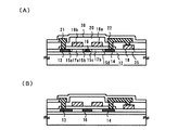
【0017】
本発明において形成する積層膜の断面構造を図1(B)に示す。図1(B)において101はガラス基板であり、102は電流制御用TFTである。さらに、103は、電流制御用TFTに電気的に接続された透明性の導電膜からなる画素電極である。画素電極103上には、EL層104を前に述べたような方法で形成する。さらに、EL層104上に、陰極105を蒸着法で形成する。
【0018】
さらに、陰極105上に窒化珪素、酸化タンタルまたは、炭素からなるDLC膜といった無機膜からなるバリア層106を形成した後、有機樹脂膜からなるカバー層107をEL層と同様の塗布方法で形成する。
【0019】
図1(C)には、EL層及びカバー層107を形成する際に電界で塗布液を制御して塗布する電界塗布法を示す。図1(C)において、110は、図1(B)に示す積層構造のうちバリア層まで形成した基板である。また、111は、カバー層を形成するための有機樹脂液が備えられている材料室である。材料室111には、超音波振動子112を設け、有機樹脂液が放出される材料室111の先端のノズル113には、電極114を設ける。
【0020】
本発明の場合、有機樹脂液は材料室111で超音波振動子112に与えられる超音波振動により霧状になる。ここで霧状になった有機樹脂液は材料室111のノズル113に設けた電極114により帯電して帯電粒子となり、アクティブマトリクス基板110上の所望の位置に成膜される。
【0021】
帯電粒子となった有機樹脂を、引き出し電極115がノズル113から引き出し、加速電極116が飛翔方向に加速し、さらに制御電極117が塗布位置を制御して基板110の所望の位置に塗布する。
【0022】
これにより、図1(B)に示すような積層構造を同一のマルチチャンバー内で形成することができ自発光装置の封止構造が完成する。
【0023】
なお、図1(B)には、EL素子を覆って、無機材料からなるバリア層を形成した後、有機材料からなるカバー層を形成した場合について示したが、本発明においては、EL素子を覆って有機材料からなるカバー層を形成した後で、無機材料からなるバリア層を形成しても良い。
【0024】
【実施例】
〔実施例1〕
本発明における自発光装置の画素部の断面図を図2に、その上面図を図3(A)に、その回路構成を図3(B)に示す。実際には画素がストライプ状に複数配列されて画素部(画像表示部)が形成される。なお、図3(A)をA−A’で切断した断面図が図2に相当する。従って図2及び図3で共通の符号を用いているので、適宜両図面を参照すると良い。また、図3の上面図では二つの画素を図示しているが、どちらも同じ構造である。
【0025】
図2において、11は基板、12は下地となる絶縁膜(以下、下地膜という)である。基板11としてはガラス、ガラスセラミックス、石英、シリコン、セラミックス、金属若しくはプラスチックでなる基板を用いることができる。
【0026】
また、下地膜12は特に可動イオンを含む基板や導電性を有する基板を用いる場合に有効であるが、石英基板には設けなくても構わない。下地膜12としては、珪素(シリコン)を含む絶縁膜を用いれば良い。なお、本明細書において「珪素を含む絶縁膜」とは、具体的には酸化珪素膜、窒化珪素膜若しくは窒化酸化珪素膜(SiOxNyで示される)など珪素、酸素若しくは窒素を所定の割合で含む絶縁膜を指す。
【0027】
また、下地膜12に放熱効果を持たせることによりTFTの発熱を発散させることはTFTの劣化又はEL素子の劣化を防ぐためにも有効である。放熱効果を持たせるには公知のあらゆる材料を用いることができる。
【0028】
ここでは画素内に二つのTFTを形成している。201はスイッチング用TFTであり、nチャネル型TFTで形成され、202は電流制御用TFTであり、pチャネル型TFTで形成されている。
【0029】
ただし、本発明において、スイッチング用TFTをnチャネル型TFT、電流制御用TFTをpチャネル型TFTに限定する必要はなく、スイッチング用TFTをpチャネル型TFT、電流制御用TFTをnチャネル型TFTにしたり、両方ともnチャネル型、又はpチャネル型TFTを用いることも可能である。
【0030】
スイッチング用TFT201は、ソース領域13、ドレイン領域14、LDD領域15a〜15d、高濃度不純物領域16及びチャネル形成領域17a、17bを含む活性層、ゲート絶縁膜18、ゲート電極19a、19b、第1層間絶縁膜20、ソース配線21並びにドレイン配線22を有して形成される。
【0031】
また、図3に示すように、ゲート電極19a、19bは別の材料(ゲート電極19a、19bよりも低抵抗な材料)で形成されたゲート配線211によって電気的に接続されたダブルゲート構造となっている。勿論、ダブルゲート構造だけでなく、シングルゲートもしくはトリプルゲート構造といったいわゆるマルチゲート構造(直列に接続された二つ以上のチャネル形成領域を有する活性層を含む構造)であっても良い。マルチゲート構造はオフ電流値を低減する上で極めて有効であり、本発明では画素のスイッチング素子201をマルチゲート構造とすることによりオフ電流値の低いスイッチング素子を実現している。
【0032】
また、活性層は結晶構造を含む半導体膜で形成される。即ち、単結晶半導体膜でも良いし、多結晶半導体膜や微結晶半導体膜でも良い。また、ゲート絶縁膜18は珪素を含む絶縁膜で形成すれば良い。また、ゲート電極、ソース配線若しくはドレイン配線としてはあらゆる導電膜を用いることができる。
【0033】
さらに、スイッチング用TFT201においては、LDD領域15a〜15dは、ゲート絶縁膜18を挟んでゲート電極19a、19bと重ならないように設ける。このような構造はオフ電流値を低減する上で非常に効果的である。
【0034】
なお、チャネル形成領域とLDD領域との間にオフセット領域(チャネル形成領域と同一組成の半導体層からなり、ゲート電圧が印加されない領域)を設けることはオフ電流値を下げる上でさらに好ましい。また、二つ以上のゲート電極を有するマルチゲート構造の場合、チャネル形成領域の間に設けられた高濃度不純物領域がオフ電流値の低減に効果的である。
【0035】
次に、電流制御用TFT202は、ソース領域31、ドレイン領域32及びチャネル形成領域34を含む活性層、ゲート絶縁膜18、ゲート電極35、第1層間絶縁膜20、ソース配線36並びにドレイン配線37を有して形成される。なお、ゲート電極35はシングルゲート構造となっているが、マルチゲート構造であっても良い。
【0036】
図2に示すように、スイッチング用TFTのドレインは電流制御用TFT202のゲートに接続されている。具体的には電流制御用TFT202のゲート電極35はスイッチング用TFT201のドレイン領域14とドレイン配線(接続配線とも言える)22を介して電気的に接続されている。また、ソース配線36は電源供給線212に接続される。
【0037】
電流制御用TFT202はEL素子203に注入される電流量を制御するための素子であるが、EL素子の劣化を考慮するとあまり多くの電流を流すことは好ましくない。そのため、電流制御用TFT202に過剰な電流が流れないように、チャネル長(L)は長めに設計することが好ましい。望ましくは一画素あたり0.5〜2μA(好ましくは1〜1.5μA)となるようにする。
【0038】
また、スイッチング用TFT201に形成されるLDD領域の長さ(幅)は0.5〜3.5μm、代表的には2.0〜2.5μmとすれば良い。
【0039】
また、図3に示すように電流制御用TFT202のゲート電極35を含む配線は、50で示される領域で電源供給線212と絶縁膜を挟んで重なる。このとき50で示される領域では、保持容量(コンデンサ)が形成される。保持容量50には半導体膜51、ゲート絶縁膜と同一層の絶縁膜(図示せず)及び電源供給線212で形成される容量も用いることが可能である。この保持容量50は、電流制御用TFT202のゲート電極35にかかる電圧を保持するためのコンデンサとして機能する。
【0040】
また、流しうる電流量を多くするという観点から見れば、電流制御用TFT202の活性層(特にチャネル形成領域)の膜厚を厚くする(好ましくは50〜100nm、さらに好ましくは60〜80nm)ことも有効である。逆に、スイッチング用TFT201の場合はオフ電流値を小さくするという観点から見れば、活性層(特にチャネル形成領域)の膜厚を薄くする(好ましくは20〜50nm、さらに好ましくは25〜40nm)ことも有効である。
【0041】
次に、38は第1パッシベーション膜であり、膜厚は10nm〜1μm(好ましくは200〜500nm)とすれば良い。材料としては、珪素を含む絶縁膜(特に窒化酸化珪素膜又は窒化珪素膜が好ましい)を用いることができる。
【0042】
第1パッシベーション膜38の上には、各TFTを覆うような形で第2層間絶縁膜(平坦化膜と言っても良い)39を形成し、TFTによってできる段差の平坦化を行う。第2層間絶縁膜39としては、有機樹脂膜が好ましく、ポリイミド、ポリアミド、アクリル樹脂、BCB(ベンゾシクロブテン)等を用いると良い。勿論、十分な平坦化が可能であれば、無機膜を用いても良い。
【0043】
第2層間絶縁膜39によってTFTによる段差を平坦化することは非常に重要である。後に形成されるEL層は非常に薄いため、段差が存在することによって発光不良を起こす場合がある。従って、EL層をできるだけ平坦面に形成しうるように画素電極を形成する前に平坦化しておくことが望ましい。
【0044】
また、40は透明導電膜でなる画素電極(EL素子の陽極に相当する)であり、第2層間絶縁膜39及び第1パッシベーション膜38にコンタクトホール(開孔)を開けた後、形成された開口部において電流制御用TFT202のドレイン配線37に接続されるように形成される。
【0045】
本実施形態では、画素電極として酸化インジウムと酸化スズの化合物でなる導電膜を用いる。また、これに少量のガリウムを添加しても良い。さらに酸化インジウムと酸化亜鉛との化合物や酸化亜鉛と酸化ガリウムの化合物を用いることもできる。
【0046】
画素電極を形成したら、樹脂材料でなるバンク41を形成する。バンクは、1〜2μm厚のアクリル樹脂または、ポリイミド膜をパターニングして形成すればよい。このバンク41は、画素列と画素列の間にストライプ状に形成される。本実施例ではソース配線21に沿って形成するがゲート配線35に沿って形成しても良い。
【0047】
次にEL層42が図1(C)で説明したような電界塗布法により形成される。
なお、ここでは一画素しか図示していないが、R(赤)、G(緑)、B(青)の各色に対応したEL層が形成される。
【0048】
EL層を形成する有機EL材料としてはポリマー系材料を用いる。代表的なポリマー系材料としては、ポリパラフェニレンビニレン(PPV)系、ポリビニルカルバゾール(PVK)系、ポリフルオレン系などが挙げられる。
【0049】
なお、PPV系有機EL材料としては様々な型のものがあるが、例えば以下のような分子式が発表されている。
(「H. Shenk,H.Becker,O.Gelsen,E.Kluge,W.Kreuder,and H.Spreitzer,“Polymers for Light Emitting Diodes”,Euro Display,Proceedings,1999,p.33-37」)
【0050】
【化1】

【化2】
また、特開平10−92576号公報に記載された分子式のポリフェニルビニルを用いることもできる。分子式は以下のようになる。
【0053】
【化3】
【化4】
また、PVK系有機EL材料としては以下のような分子式がある。
【0056】
【化5】
ポリマー系有機EL材料はポリマーの状態で溶媒に溶かして塗布することもできるし、モノマーの状態で溶媒に溶かして塗布した後に重合することもできる。モノマーの状態で塗布した場合、まずポリマー前駆体が形成され、真空中で加熱することにより重合してポリマーになる。
【0058】
具体的なEL層としては、赤色に発光するEL層にはシアノポリフェニレンビニレン、緑色に発光するEL層にはポリフェニレンビニレン、青色に発光するEL層にはポリフェニレンビニレン若しくはポリアルキルフェニレンを用いれば良い。膜厚は30〜150nm(好ましくは40〜100nm)とすれば良い。
【0059】
但し、以上の例は本発明のEL層として用いることのできる有機EL材料の一例であって、これに限定する必要はまったくない。本発明では有機EL材料と溶媒との混合物を電界塗布方式により塗布して、溶媒を揮発させて除去することによりEL層を形成する。従って、溶媒を揮発させる際にEL層のガラス転移温度を超えない組み合わせであれば如何なる有機EL材料を用いても良いし、ここでは述べなかったような低分子EL材料を用いたり、低分子材料と高分子材料を併せて用いて形成させても良い。
【0060】
また、代表的な溶媒としてはトルエン、キシレン、クロロベンゼン、ジクロロベンゼン、アニソール、クロロフォルム、ジクロロメタン、γブチルラクトン、ブチルセルソルブ、シクロヘキサン、NMP(N−メチル−2−ピロリドン)、シクロヘキサノン、ジオキサンまたは、THF(テトラヒドロフラン)が挙げられる。なお、前出のEL材料を上記の溶媒に溶解させた溶液を本明細書中では、塗布液と呼ぶ。また、塗布液の粘性は、1×10⁻³〜3×10⁻²Pa・sであることが好ましい。
【0061】
まず、図1(C)に示すように材料室111に備えられた塗布液が超音波振動子112により霧状になる。これがノズル113に設けられている電極114による電界の影響で塗布液が帯電粒子となると引き出し電極115によりノズル113から引き出される。引き出された塗布液は、加速電極116により加速された後、制御電極117により制御され所望の位置に塗布される。これによりEL層を形成する。なお、この塗布液が材料室111から飛び出す瞬間にノズル113に取り付けられている電極114に与えられる電界の影響で塗布液が帯電し、帯電粒子となる。
【0062】
本発明においては、まず、材料室111に備えられている赤色EL層用塗布液を霧状にして電界で制御して塗布することで、画素上の赤色に発光する画素列を形成することができる。次に基板を隣の画素列方向に3列分移動しながら2列おきに赤色に発光する画素列を形成する。次に、材料室111に備えられている緑色EL層用塗布液を同様に塗布させ、緑色に発光すべき画素列を2列おきに形成する。さらに材料室111に備えられている青色EL層用塗布液を同様に塗布させ、青色に発光すべき画素列を形成する。
【0063】
以上の操作を行うことで、赤、緑、青と3列にストライプ状に並んだ画素列を基板上に複数形成させることができる。
【0064】
なお、EL層用塗布液を備えている材料室111は、EL層用塗布液の種類を変える度に一緒に変えても良いし、材料室を変えずにEL層用塗布液のみを入れ替えて用いても良い。また、材料室111に取り付けられているノズル113は、一つに限られることはなく二つ以上であっても良い。
【0065】
また、ここでは用いていないが材料室111と基板の間にマスクを備えてマスクを介して基板上に塗布液が塗布される位置を制御してもよい。なお、材料室111及びマスクを別々に設けても良いが、一体形成して装置化しても良い。
【0066】
さらに、EL層42を形成する際、EL層は水分や酸素の存在によって容易に劣化してしまうため、処理雰囲気は水分や酸素の少ない雰囲気とし、窒素やアルゴンといった不活性ガス中で行うことが望ましい。さらに処理雰囲気としては、塗布液の蒸発速度を制御できることから塗布液作製に用いた溶媒雰囲気にするのも良い。
【0067】
以上のようにしてEL層42を形成したら、次に遮光性導電膜からなる陰極43及び保護電極が形成される。本実施例では陰極43として、MgAgからなる導電膜を用い、保護電極44としてアルミニウムからなる導電膜を用いる。
【0068】
なお、上述のようにEL層は熱に弱いので、陰極43はなるべく低温(好ましくは室温から120℃までの温度範囲)で成膜するのが望ましい。従って、プラズマCVD法、スパッタリング法が望ましい成膜方法といえる。又、ここまで完成したものを本明細書中では、アクティブマトリクス基板という。
【0069】
本発明においては、このアクティブマトリクス基板上に窒化珪素、酸化タンタル及びまたは炭素といった無機膜からなるバリア層45を形成させた後、有機樹脂膜からなるカバー層46を図1(C)で説明したような電界塗布法で形成する。このときカバー層46を形成するために用いる有機樹脂液の粘性は、1×10⁻³〜3×10⁻²Pa・sであることが好ましい。又、このとき形成されるカバー層の膜厚は0.1μm〜20μmが好ましいが、塗布と乾燥を繰り返すことで膜厚をこれ以上に厚くすることも可能である。
【0070】
カバー層46を形成させた時点で自発光装置の封止が完了したことになるが、カバー層46の上にガラス基板、石英基板またはプラスチック基板といった封止基板を設けて封止構造を完成してもよい。なお、このときカバー層46にアクティブマトリクス基板と封止基板を密着させるための接着剤としての役割を持たせても良い。
【0071】
なお、ここでEL層の劣化の原因となる水分または酸素に対する対策として有機樹脂膜からなるカバー層内に酸化バリウムといった乾燥剤や酸化防止剤を加えておくことも可能である。
【0072】
〔実施例2〕
本発明の実施例における画素部とその周辺に設けられる駆動回路部のTFTを同時に作製する方法について図4〜図6を用いて説明する。但し、説明を簡単にするために、駆動回路に関しては基本回路であるCMOS回路を図示することとする。
【0073】
まず、図4(A)に示すように、ガラス基板300上に下地膜301を300nmの厚さに形成する。本実施例では下地膜301として100nm厚の窒化酸化珪素膜と200nmの窒化酸化珪素膜とを積層して用いる。この時、ガラス基板300に接する方の窒素濃度を10〜25wt%としておくと良い。もちろん下地膜を設けずに石英基板上に直接素子を形成しても良い。
【0074】
次に下地膜301の上に50nmの厚さの非晶質珪素膜(図示せず))を公知の成膜法で形成する。なお、非晶質珪素膜に限定する必要はなく、非晶質構造を含む半導体膜(微結晶半導体膜を含む)であれば良い。さらに非晶質シリコンゲルマニウム膜などの非晶質構造を含む化合物半導体膜でも良い。また、膜厚は20〜100nmの厚さであれば良い。
【0075】
そして、公知の技術により非晶質珪素膜を結晶化し、結晶質珪素膜(多結晶シリコン膜若しくはポリシリコン膜ともいう)302を形成する。公知の結晶化方法としては、電熱炉を使用した熱結晶化方法、レーザー光を用いたレーザーアニール結晶化法、赤外光を用いたランプアニール結晶化法がある。本実施例では、XeClガスを用いたエキシマレーザー光を用いて結晶化する。
【0076】
なお、本実施例では線状に加工したパルス発振型のエキシマレーザー光を用いるが、矩形であっても良いし、連続発振型のアルゴンレーザー光や連続発振型のエキシマレーザー光を用いることもできる。
【0077】
本実施例では結晶質珪素膜をTFTの活性層として用いるが、非晶質珪素膜を用いることも可能である。また、オフ電流を低減する必要のあるスイッチング用TFTの活性層を非晶質珪素膜で形成し、電流制御用TFTの活性層を結晶質珪素膜で形成することも可能である。非晶質珪素膜はキャリア移動度が低いため電流を流しにくくオフ電流が流れにくい。即ち、電流を流しにくい非晶質珪素膜と電流を流しやすい結晶質珪素膜の両者の利点を生かすことができる。
【0078】
次に、図4(B)に示すように、結晶質珪素膜302上に酸化珪素膜でなる保護膜303を130nmの厚さに形成する。この厚さは100〜200nm(好ましくは130〜170nm)の範囲で選べば良い。また、珪素を含む絶縁膜であれば他の膜でも良い。この保護膜303は不純物を添加する際に結晶質珪素膜が直接プラズマに曝されないようにするためと、微妙な濃度制御を可能にするために設ける。
【0079】
そして、その上にレジストマスク304a、304bを形成し、保護膜303を介してn型を付与する不純物元素(以下、n型不純物元素という)を添加する。なお、n型不純物元素としては、代表的には15族に属する元素、典型的にはリン又は砒素を用いることができる。なお、本実施例ではホスフィン(PH3)を質量分離しないでプラズマ励起したプラズマ(イオン)ドーピング法を用い、リンを1×10¹⁸atoms/cm3の濃度で添加する。勿論、質量分離を行うイオンインプランテーション法を用いても良い。
【0080】
この工程により形成されるn型不純物領域305には、n型不純物元素が2×10¹⁶〜5×10¹⁹atoms/cm3(代表的には5×1017〜5×1018atoms/cm3)の濃度で含まれるようにドーズ量を調節する。
【0081】
次に、図4(C)に示すように、保護膜303およびレジスト304a、304bを除去し、添加した15族に属する元素の活性化を行う。活性化手段は公知の技術を用いれば良いが、本実施例ではエキシマレーザー光の照射により活性化する。勿論、パルス発振型でも連続発振型でも良いし、エキシマレーザー光に限定する必要はない。但し、添加された不純物元素の活性化が目的であるので、結晶質珪素膜が溶融しない程度のエネルギーで照射することが好ましい。なお、保護膜303をつけたままレーザー光を照射しても良い。
【0082】
なお、このレーザー光による不純物元素の活性化に際して、熱処理による活性化を併用しても構わない。熱処理による活性化を行う場合は、基板の耐熱性を考慮して450〜550℃程度の熱処理を行えば良い。
【0083】
この工程によりn型不純物領域305の端部、即ち、n型不純物領域305、の周囲に存在するn型不純物元素を添加していない領域との境界部(接合部)が明確になる。このことは、後にTFTが完成した時点において、LDD領域とチャネル形成領域とが非常に良好な接合部を形成しうることを意味する。
【0084】
次に、図4(D)に示すように、結晶質珪素膜の不要な部分を除去して、島状の半導体膜(以下、活性層という)306〜309を形成する。
【0085】
次に、図4(E)に示すように、活性層306〜309を覆ってゲート絶縁膜310を形成する。ゲート絶縁膜310としては、10〜200nm、好ましくは50〜150nmの厚さの珪素を含む絶縁膜を用いれば良い。これは単層構造でも積層構造でも良い。本実施例では110nm厚の窒化酸化珪素膜を用いる。
【0086】
次に、200〜400nm厚の導電膜を形成し、パターニングしてゲート電極311〜315を形成する。このゲート電極311〜315の端部をテーパー状にすることもできる。なお、本実施例ではゲート電極と、ゲート電極に電気的に接続された引き回しのための配線(以下、ゲート配線という)とを別の材料で形成する。具体的にはゲート電極よりも低抵抗な材料をゲート配線として用いる。これは、ゲート電極としては微細加工が可能な材料を用い、ゲート配線には微細加工はできなくとも配線抵抗が小さい材料を用いるためである。勿論、ゲート電極とゲート配線とを同一材料で形成しても構わない。
【0087】
また、ゲート電極は単層の導電膜で形成しても良いが、必要に応じて二層、三層といった積層膜とすることが好ましい。ゲート電極の材料としては公知のあらゆる導電膜を用いることができる。ただし、上述のように微細加工が可能、具体的には2μm以下の線幅にパターニング可能な材料が好ましい。
【0088】
代表的には、タンタル(Ta)、チタン(Ti)、モリブデン(Mo)、タングステン(W)、クロム(Cr)、シリコン(Si)から選ばれた元素でなる膜、または前記元素の窒化物膜(代表的には窒化タンタル膜、窒化タングステン膜、窒化チタン膜)、または前記元素を組み合わせた合金膜(代表的にはMo−W合金、Mo−Ta合金)、または前記元素のシリサイド膜(代表的にはタングステンシリサイド膜、チタンシリサイド膜)を用いることができる。勿論、単層で用いても積層して用いても良い。
【0089】
本実施例では、50nm厚の窒化タンタル(TaN)膜と、350nm厚のタンタル(Ta)膜とからなる積層膜を用いる。これはスパッタ法で形成すれば良い。また、スパッタガスとしてXe、Ne等の不活性ガスを添加すると応力による膜はがれを防止することができる。
【0090】
またこの時、ゲート電極312はn型不純物領域305の一部とゲート絶縁膜310を挟んで重なるように形成する。この重なった部分が後にゲート電極と重なったLDD領域となる。なお、ゲート電極313,314は、断面では、二つに見えるが実際には電気的に接続されている。
【0091】
次に、図5(A)に示すように、ゲート電極311〜315をマスクとして自己整合的にn型不純物元素(本実施例ではリン)を添加する。こうして形成される不純物領域316〜323にはn型不純物領域305の1/2〜1/10(代表的には1/3〜1/4)の濃度でリンが添加されるように調節する。具体的には、1×1016〜5×1018atoms/cm3(典型的には3×1017〜3×1018atoms/cm3)の濃度が好ましい。
【0092】
次に、図5(B)に示すように、ゲート電極等を覆う形でレジストマスク324a〜324dを形成し、n型不純物元素(本実施例ではリン)を添加して高濃度にリンを含む不純物領域325〜329を形成する。ここでもホスフィン(PH3)を用いたイオンドープ法で行い、この領域のリンの濃度は1×10²⁰〜1×10²¹atoms/cm3(代表的には2×1020〜5×1021atoms/cm3)となるように調節する。
【0093】
この工程によってnチャネル型TFTのソース領域若しくはドレイン領域が形成されるが、スイッチング用TFTでは、図5(A)の工程で形成したn型不純物領域319〜321の一部を残す。この残された領域が、図5におけるスイッチング用TFT201のLDD領域15a〜15dに対応する。
【0094】
次に、図5(C)に示すように、レジストマスク324a〜324dを除去し、新たにレジストマスク332を形成する。そして、p型不純物元素(本実施例ではボロン)を添加し、高濃度にボロンを含む不純物領域333〜336を形成する。ここではジボラン(B2H6)を用いたイオンドープ法により3×10²⁰〜3×10²¹atoms/cm3(代表的には5×1020〜1×1021atoms/cm3)の濃度となるようにボロンを添加する。
【0095】
なお、不純物領域333〜336には既に1×10²⁰〜1×10²¹atoms/cm3の濃度でリンが添加されているが、ここで添加されるボロンはその少なくとも3倍以上の濃度で添加される。そのため、予め形成されていたn型の不純物領域は完全にp型に反転し、p型の不純物領域として機能する。
【0096】
次に、レジストマスク332を除去した後、それぞれの濃度で添加されたn型またはp型不純物元素を活性化する。活性化手段としては、ファーネスアニール法、レーザーアニール法、またはランプアニール法で行うことができる。本実施例では電熱炉において窒素雰囲気中、550℃、4時間の熱処理を行う。
【0097】
このとき雰囲気中の酸素を極力排除することが重要である。なぜならば酸素が少しでも存在していると露呈したゲート電極の表面が酸化され、抵抗の増加を招くと共に後にオーミックコンタクトを取りにくくなるからである。従って、上記活性化工程における処理雰囲気中の酸素濃度は1ppm以下、好ましくは0.1ppm以下とすることが望ましい。
【0098】
次に、活性化工程が終了したら図5(D)に示すように300nm厚のゲート配線337を形成する。ゲート配線337の材料としては、アルミニウム(Al)又は銅(Cu)を主成分(組成として50〜100%を占める。)とする金属を用いれば良い。配置としては図3のようにゲート配線211とスイッチング用TFTのゲート電極19a、19b(図4(E)の313、314)が電気的に接続するように形成する。
【0099】
このような構造とすることでゲート配線の配線抵抗を非常に小さくすることができるため、面積の大きい画像表示領域(画素部)を形成することができる。即ち、画面の大きさが対角10インチ以上(さらには30インチ以上)の自発光装置を実現する上で、本実施例の画素構造は極めて有効である。
【0100】
次に、図6(A)に示すように、第1層間絶縁膜338を形成する。第1層間絶縁膜338としては、珪素を含む絶縁膜を単層で用いるか、2種類以上の珪素を含む絶縁膜を組み合わせた積層膜を用いれば良い。また、膜厚は400nm〜1.5μmとすれば良い。本実施例では、200nm厚の窒化酸化珪素膜の上に800nm厚の酸化珪素膜を積層した構造とする。
【0101】
さらに、3〜100%の水素を含む雰囲気中で、300〜450℃で1〜12時間の熱処理を行い、水素化処理をする。この工程は熱的に励起された水素により半導体膜の不対結合手を水素終端する工程である。水素化の他の手段として、プラズマ水素化(プラズマ化して生成された水素を用いる)を行っても良い。
【0102】
なお、水素化処理は第1層間絶縁膜338を形成する間に入れても良い。即ち、200nm厚の窒化酸化珪素膜を形成した後で上記のように水素化処理を行い、その後で残り800nmの膜厚の酸化珪素膜を形成してもよい。
【0103】
次に、第1層間絶縁膜338及びゲート絶縁膜310に対してコンタクトホールを形成し、ソース配線339〜342と、ドレイン配線343〜345を形成する。なお、本実施例ではこの電極を、Ti膜を100nm、Tiを含むアルミニウム膜を300nm、Ti膜150nmをスパッタ法で連続形成した3層構造の積層膜とする。勿論、他の導電膜でも良い。
【0104】
次に、50〜500nm(代表的には200〜300nm)の厚さで第1パッシベーション膜346を形成する。本実施例では第1パッシベーション膜346として300nm厚の窒化酸化珪素膜を用いる。これは窒化珪素膜で代用しても良い。
【0105】
なお、窒化酸化珪素膜の形成に先立ってH2、NH3等水素を含むガスを用いてプラズマ処理を行うことは有効である。この前処理により励起された水素が第1層間絶縁膜338に供給され、熱処理を行うことで、第1パッシベーション膜346の膜質が改善される。それと同時に、第1層間絶縁膜338に添加された水素が下層側に拡散するため、効果的に活性層を水素化することができる。
【0106】
次に、図6(B)に示すように有機樹脂からなる第2層間絶縁膜347を形成する。有機樹脂としてはポリイミド、ポリアミド、アクリル樹脂またはBCB(ベンゾシクロブテン)といった材料を使用することができる。特に、第2層間絶縁膜347は平坦化の意味合いが強いので、平坦性に優れたアクリル樹脂が好ましい。本実施例ではTFTによって形成される段差を十分に平坦化しうる膜厚でアクリル樹脂膜を形成する。好ましくは1〜5μm(さらに好ましくは2〜4μm)とすれば良い。
【0107】
次に、第2層間絶縁膜347及び第1パッシベーション膜346に対してコンタクトホールを形成し、ドレイン配線345と電気的に接続する画素電極348を形成する。本実施例では酸化インジウム・スズ(ITO)膜を110nmの厚さに形成し、パターニングを行って画素電極とする。また、酸化インジウムに2〜20%の酸化亜鉛(ZnO)を混合した化合物や、酸化亜鉛と酸化ガリウムからなる化合物を透明電極として用いても良い。この画素電極がEL素子の陽極となる。
【0108】
次に、図6(C)に示すように、樹脂材料からなるバンク349を形成する。バンク349は合計で1〜2μmの膜厚のアクリル樹脂膜またはポリイミド膜といった膜をパターニングして形成すれば良い。このバンク349は図6に示したように、画素と画素との間にストライプ状に形成する。本実施例ではソース配線341に沿って形成するがゲート配線337に沿って形成しても良い。
【0109】
次に、EL層350を、図1(C)で説明した電界塗布法により形成する。なお、ここでは一画素しか図示していないが、実施例1で説明したようにR(赤)、G(緑)、B(青)の各色に対応したEL層をそれぞれ形成する。
【0110】
まず、材料室に備えられたEL層用塗布液を超音波振動子による超音波振動で霧状にする。この霧状のEL層用塗布液を電極にかけられた電圧が与える電界で帯電させると、材料室の外部に設けられた引き出し電極により引き出すことができる。引き出されたEL層用塗布液は、加速電極により飛翔方向に加速された後、制御電極で制御して、基板110上の所望の位置に塗布することができる。
【0111】
本発明においては、まず、材料室から赤色EL層用塗布液を霧状のEL層用塗布液として引き出し電極により引き出し、加速電極により加速した後、制御電極により制御して、画素上の赤色に発光する画素列にEL層を形成する。次に基板を横方向に移動した後、材料室から緑色EL層用塗布液を塗布し、緑色に発光すべき画素列を形成する。さらに基板を横方向に移動して材料室から青色EL層用塗布液を塗布し、青色に発光すべき画素列を形成する。
【0112】
以上のように、基板を移動しながら赤、緑、青色に発光する画素列を順次塗布することで3色のストライプ状のEL層を形成する。なお、本実施例では一画素しか図示されていないが、同じ色に発光するEL層は、一列ずつ形成しても良いし、同時に形成しても良い。また、必要に応じては、材料室と基板の間にマスクを設けたり、マスクに電界をかけて塗布液の塗布位置を制御することも可能である。
【0113】
本実施例では、EL材料としては、赤色に発光するEL層にはシアノポリフェニレンビニレン、緑色に発光するEL層にはポリフェニレンビニレン、青色に発光するEL層にはポリフェニレンビニレン若しくはポリアルキルフェニレンを用いれば良い。膜厚は30〜150nm(好ましくは40〜100nm)とすれば良い。
【0114】
EL層350としては公知の材料を用いることができる。公知の材料としては、駆動電圧を考慮すると有機材料を用いるのが好ましい。なお、本実施例ではEL層350は、上記EL材料から形成される、いわゆる発光層のみの単層構造とするが、必要に応じて電子注入層、電子輸送層、正孔輸送層、正孔注入層、電子阻止層もしくは正孔素子層を設けても良い。また、本実施例ではEL素子の陰極351としてMgAg電極を用いた例を示すが、公知の他の材料であっても良い。
【0115】
本実施例では、電界制御による電界塗布法を示したが、インクジェット法やEL層用材料を荷電粒子として制御して塗布する方法を用いても良い。
【0116】
なお、発光層は、各色ごとに塗布され形成されるが、電子注入層、電子輸送層、正孔輸送層、正孔注入層、電子阻止層もしくは正孔素子層を形成する場合は、発光層を形成する材料が異なっていても、関係なく同一材料をスピンコート法、塗布法といった方法を用いて、一度に形成してもよい。
【0117】
EL層350を形成した後、陰極(MgAg電極)351を真空蒸着法により形成する。なお、EL層350の膜厚は80〜200nm(典型的には100〜120nm)、陰極351の厚さは180〜300nm(典型的には200〜250nm)とすれば良い。
【0118】
さらに、陰極351上には、保護電極352を設ける。保護電極352としてはアルミニウムを主成分とする導電膜を用いると良い。保護電極352は、マスクを用いて真空蒸着法で形成すると良い。なお、基板上に保護電極まで形成した状態を本明細書中では、アクティブマトリクス基板という。
【0119】
保護電極352まで完成したアクティブマトリクス基板上には、さらに外気に曝されないようにして、バリア層353を形成する。本実施例においては、バリア層353を形成する材料として酸化タンタルを用いるが、窒化珪素、窒化アルミニウムもしくは炭素膜、具体的にはDLC膜といった無機材料を用いても良い。また、本実施例においてバリア層353は、スパッタリング法を用いて形成するが、プラズマCVD法といった室温で成膜できる方法を用いることもできる。
【0120】
バリア層353を形成したら、バリア層353の上に有機樹脂からなるカバー層354を形成する。なお、有機樹脂を溶媒に溶解したり、有機樹脂自体の粘度を適度に調節して有機樹脂液を作製した後、これを材料室に備えて電界塗布法により塗布し、カバー層354を形成する。このとき有機樹脂液の粘性は、1×10⁻³〜3×10⁻²Pa・sであることが好ましい。
【0121】
また、この時カバー層を形成する有機樹脂液の内部に酸化バリウムといった吸湿剤や酸化防止剤を加えるとEL素子の劣化原因である水分や酸素の進入を防ぐのに効果的である。
【0122】
本実施例の場合は、図6(C)に示すように、nチャネル型205の活性層は、ソース領域355、ドレイン領域356、LDD領域357及びチャネル形成領域358を含み、LDD領域357はゲート絶縁膜310を挟んでゲート電極312と重なっている。
【0123】
ドレイン領域側のみにLDD領域を形成しているのは、動作速度を落とさないための配慮である。また、このnチャネル型TFT205はオフ電流値をあまり気にする必要はなく、それよりも動作速度を重視した方が良い。従って、LDD領域357は完全にゲート電極に重ねてしまい、極力抵抗成分を少なくすることが望ましい。即ち、いわゆるオフセットはなくした方がよい。
【0124】
ところで、本実施例のアクティブマトリクス基板は、画素部だけでなく駆動回路部にも最適な構造のTFTを配置することにより、非常に高い信頼性を示し、動作特性も向上しうる。
【0125】
まず、極力動作速度を落とさないようにホットキャリア注入を低減させる構造を有するTFTを、駆動回路部を形成するCMOS回路のnチャネル型TFT205として用いる。なお、ここでいう駆動回路としては、シフトレジスタ、バッファ、レベルシフタ、サンプリング回路(サンプル及びホールド回路)などが含まれる。デジタル駆動を行う場合には、D/Aコンバータなどの信号変換回路も含まれうる。
【0126】
次に、画素部のTFTとして、nチャネル型のスイッチング用TFTの断面構造を図7により説明する。なお、ここで用いた符号は、図2で用いた符号と対応している。
【0127】
まず、図7に示したスイッチング用TFTであるが、図7(A)は、LDD領域15a〜15dがゲート絶縁膜18を挟んでデート電極19a及び19bと重ならないように設けられている。このような構造は、オフ電流値を低減する上で非常に効果的である。
【0128】
これに対して、図7(B)には、これらのLDD領域15a〜15dは設けられていない。図7(B)の構造とする場合には、図7(A)の構造を形成させる場合に比べて工程を減らすことができるので生産効率を向上することができる。
【0129】
本発明において、スイッチング用TFTとしては、図7(A)及び図7(B)のどちらの構造を用いても良い。
【0130】
次に、画素部のTFTとして、図8には、nチャネル型の電流制御用TFTの断面構造図を示す。なお、ここで用いた符号は、図2で用いた符号と対応している。
【0131】
図8(A)に示した電流制御用TFTにおいて、ドレイン領域32とチャネル形成領域34との間にLDD領域33が設けられる。ここでは、LDD領域33がゲート絶縁膜18を挟んでゲート電極35に重なっている領域と重なっていない領域とを有する構造を示したが、図8(B)に示すようにLDD領域33を設けない構造としてもよい。
【0132】
電流制御用TFTは、EL素子を発光させるための電流を供給すると同時に、その供給量を制御して階調表示を可能とする。そのため、電流を流しても劣化しないようにホットキャリア注入による劣化対策を講じておく必要がある
【0133】
ホットキャリア注入による劣化に関しては、ゲート電極に対してLDD領域が重なった構造が非常に効果的であることが知られている。そのため、図8(A)に示したようにゲート絶縁膜18を挟んでゲート電極35に重なっている領域にLDD領域を設けるという構造が適当であるが、ここではオフ電流対策としてゲート電極に重ならないLDD領域も設けるという構造を示した。しかし、ゲート電極に重ならないLDD領域は、必ずしも設けなくて良い。また、場合によっては、図8(B)に示すようにこれらのLDD領域を設けなくても良い。
【0134】
さらに、図8に示したTFT構造において、TFTにかかる電圧VDSが10V以上であるときには、図8(A)で示した構造が好ましいがTFTにかかる電圧VDSが10Vに満たない場合には図8(B)で示す構造が好ましい。
【0135】
なお、図6(C)で示すカバー層354まで形成して気密性を高めたら、絶縁体上に形成された素子又は回路から引き回された端子と外部信号端子とを接続するためのコネクター(フレキシブルプリントサーキット:FPC)を取り付けて製品として完成する。このような出荷できる状態にまでした状態を本明細書中では自発光装置(またはELモジュール)をという。
【0136】
ここで、カバー層まで形成した本実施例のELモジュールについて図9(A)、(B)を用いて説明する。
【0137】
本実施例のアクティブマトリクス型自発光装置は、ガラス基板901上に形成された、画素部902と、ゲート側駆動回路903と、ソース側駆動回路904を含む。画素部のスイッチング用TFT905はnチャネル型TFTであり、ゲート側駆動回路903に接続されたゲート配線906、ソース側駆動回路904に接続されたソース配線907の交点に配置されている。また、スイッチング用TFT905のドレインは電流制御用TFT908のゲートに接続されている。
【0138】
さらに、電流制御用TFT908のソース側は電源供給線909に接続される。本実施例のような構造では、電源供給線909には接地電位(アース電位)が与えられている。また、電流制御用TFT908のドレインにはEL素子910が接続されている。また、このEL素子910の陽極には所定の電圧(3〜12V、好ましくは3〜5V)が加えられる。
【0139】
そして、外部入出力端子となるFPC911には駆動回路部まで信号を伝達するための接続配線912、913、及び電源供給線909に接続された接続配線914が設けられている。
【0140】
ここで、図9(A)をA−A’で切断した断面図を図9(B)に示す。なお、図9(A)、(B)では同一の部位に同一の符号を用いている。一部には、図6と同一の部位に同一の符号を用いている。
【0141】
図9(B)に示すように、基板901上には画素部902、ゲート側駆動回路903を形成し、画素部902は電流制御用TFT202とそれに電気的に接続された画素電極348を含む複数の画素により形成する。また、ゲート側駆動回路903はnチャネル型TFT205とpチャネル型TFT206とを相補的に組み合わせたCMOS回路を用いて形成する。
【0142】
画素電極348はEL素子の陽極として機能する。また、画素電極348間の隙間にはバンク349を形成し、バンク349の内側にEL層350を形成する。また、その上に陰極351及び保護電極352を形成する。なおここで示したEL素子の構造に限られる必要はなく素子構造を反対とし、画素電極を陰極としても構わない。
【0143】
本実施例の場合、保護電極352は画素列ごとに共通の配線としても機能し、接続配線912を経由してFPC911に電気的に接続されている。さらに、画素部902及びゲート側駆動回路903に含まれる素子は全て窒化珪素、酸化タンタルもしくは炭素(具体的にはDLC膜)といった無機材料からなるバリア層で覆われている。このバリア層353は省略することも可能であるが、各素子を外部と遮断する上で設けた方が好ましい。
【0144】
次に、バリア層の上には、EL素子を覆うようにしてカバー層916を設ける。カバー層916としては、PVC(ポリビニルクロライド)、エポキシ樹脂、シリコン樹脂、アクリル樹脂、PVB(ポリビニルブチラル)またはEVA(エチレンビニルアセテート)を用いることができる。このカバー層916の内部に乾燥剤(図示せず)を設けておくと、吸湿効果を保ち続けられるので好ましい。
【0145】
また、カバー層916の上には、ガラス、プラスチック、およびセラミックスでなる保護基板を設けることができる。さらに、カバー層916を用いて保護基板(図示せず)を接着する構造としても良い。
【0146】
以上のようにEL素子910上にバリア層353及びカバー層916を設けることにより、EL素子910を外部から完全に遮断することができ、外部から水分や酸素等のEL層の酸化による劣化を促す物質が侵入することを防ぐことができる。従って、信頼性の高い自発光装置を作製することができる。
【0147】
また、図9に示した自発光装置の回路構成の一例を図10に示す。本実施例の自発光装置は、ソース側駆動回路1001、ゲート側駆動回路(A)1007、ゲート側駆動回路(B)1011、画素部1006を有している。なお、本明細書中において、駆動回路部とはソース側処理回路およびゲート側駆動回路を含めた総称である。
【0148】
ソース側駆動回路1001は、シフトレジスタ1002、レベルシフタ1003、バッファ1004、サンプリング回路(サンプル及びホールド回路)1005を備えている。また、ゲート側駆動回路(A)1007は、シフトレジスタ1008、レベルシフタ1009、バッファ1010を備えている。ゲート側駆動回路(B)1011も同様な構成である。
【0149】
ここでシフトレジスタ1002、1008は駆動電圧が5〜16V(代表的には10V)であり、回路を形成するCMOS回路に使われるnチャネル型TFTは図6(C)の205で示される構造が適している。
【0150】
また、レベルシフタ1003、1009、バッファ1004、1010はシフトレジスタと同様に、図6(C)のnチャネル型TFT205を含むCMOS回路が適している。なお、ゲート配線をダブルゲート構造、トリプルゲート構造といったマルチゲート構造とすることは、各回路の信頼性を向上させる上で有効である。また、画素部1006は図2に示した構造の画素を配置する。
【0151】
なお、上記構成は、図4〜6に示した作製工程に従ってTFTを作製することによって容易に実現することができる。また、本実施例では画素部と駆動回路部の構成のみ示しているが、本実施例の作製工程に従えば、その他にも信号分割回路、D/Aコンバータ回路、オペアンプ回路、γ補正回路など駆動回路以外の論理回路を同一絶縁体上に形成することが可能であり、さらにはメモリ部やマイクロプロセッサ等を形成しうると考えている。
【0152】
また、本実施例の構成は、実施例1の構成と自由に組み合わせることができる。
【0153】
〔実施例3〕
ここでは、図1(B)で示したのと異なる積層構造の作製について説明する。図11において、基板1100上に電流制御用TFT101を形成し、電流制御用TFT1101に電気的に接続された画素電極1102を図のように形成する。画素電極1102上には、EL層1103を形成するが、本実施例ではインクジェット法を用いる。なお、本実施例で用いるEL層用塗布液は、実施例1で用いたものと同様の材料を用いるとよい。
【0154】
次にEL層1103の上に、蒸着法を用いて陰極1104を形成する。なお陰極には、MgAgやAl−Liといった仕事関数の低い材料を用いると良い。陰極1104を形成した後で再びインクジェト法により有機樹脂膜からなるカバー層1105を画素部に均一に成膜する。なお、成膜するカバー層1105の膜厚は10nm〜300nmが好ましい。
【0155】
また、有機樹脂からなるカバー層1105を形成する材料としては、硬度が高く、水分または酸素といった物質を通しにくく、平坦性のある材料を用いると良い。具体的には、エポキシ樹脂、アクリル樹脂、ポリイミド、ポリアミドおよびシリコン樹脂といった有機樹脂が好ましい。なお、カバー層1105の形成にはインクジェット法を用いることから画素部分に選択的に形成することができる。
【0156】
図12には、インクジェット法でアクティブマトリクス基板1200上の画素部1201にカバー層1202を形成する方法を示す。なお、ここに示す構造のヘッド1203からEL層を形成する塗布液やカバー層を形成する有機樹脂液を吐出する。なお、インクジェット法で知られるピエゾ方式には、MLP(Multi Layer Piezo)タイプとMLChip(Multi Layer Ceramic Hyper Integrated Piezo Segments)タイプがあるが、ここで示すヘッド1203は、セイコーエプソン社製のオンデマンドピエゾ駆動MLChip方式と呼ばれるヘッドである。
【0157】
MLChipとは、セラミックでなる振動板1204、連通板1205、及び材料室板1206で材料室1207を形成し、振動板1204上にピエゾ素子1208を各材料室に対応して形成したアクチュエーターである。
【0158】
そして、このMLChipに3枚のステンレスプレート(SUSプレート)を積層して、供給孔1209、リザーバー1210、ノズル1211を形成しヘッド1203を形成する。なお図12には、ノズル1211が二つ設けられている様子を示すが、ノズルの数はこれに限られることはなく塗布する領域や塗布液によって一つであっても良いし、三つ以上設けられていても良い。
【0159】
このMLChipからなる塗布装置の動作原理は、上部電極1212及び下部電極1213に電圧がかけられた際に、ピエゾ素子1208が振動することによるピエゾ素子1208と振動板1204の圧電効果であり、撓み振動である。つまり、この撓みにより材料室1207に圧力がかかり、材料室1207に備えられている有機樹脂液が押し出され、塗布がなされる。
【0160】
図11に示すようにカバー層1105を形成した後、スパッタリング法を用いてカバー層1105を覆うようにバリア層1106を形成する。本実施例では、バリア層1106を炭素膜、具体的にはDLC膜(ダイヤモンドライクカーボン)により形成する。しかし、バリア層1106を形成する材料は、これに限定する必要はなく、酸化タンタル、窒化アルミニウムまたは窒化珪素などを用いても良い。なお、バリア層1106はシャドウマスクを用いて選択的に形成する。
【0161】
以上のようにカバー層1105及びバリア層1106をアクティブマトリクス基板上に形成することで、外部からEL素子の劣化原因となる水分や酸素の進入を防ぐことができる。
【0162】
〔実施例4〕
本実施例では本発明をパッシブ型(単純マトリクス型)の自発光装置に用いた場合について説明する。説明には図13を用いる。図13において、1301はプラスチックからなる基板、1302は透明性の導電膜からなる陽極である。本実施例では、陽極1302として酸化インジウムと酸化亜鉛との化合物をスパッタリング法により形成する。なお、図13では図示されていないが、複数本の陽極1302が紙面と平行な方向へストライプ状に配列されている。
【0163】
また、ストライプ状に配列された陰極1305を紙面に垂直な方向に形成し、さらに陰極1305の間を埋めるようにバンク1303を形成する。
【0164】
次に、EL材料からなるEL層1304a〜1304cを実施例1で示した電界塗布法により形成する。なお、1304aは赤色に発光するEL層、1304bは緑色に発光するEL層、1304cは青色に発光するEL層である。用いる有機EL材料は実施例1と同様のものを用いれば良い。これらのEL層はバンク1303が形成する溝に沿って形成されるため、紙面に垂直な方向にストライプ状に形成される。
【0165】
本実施例を実施することにより、基板上に赤、緑、青の三色の画素をストライプ状に形成する。なお、画素の色は、必ずしも三色である必要はなく、一色または、二色であってもよい。また、色は、赤、緑、青に限られることはなく、黄色、オレンジ、グレーといった発色することが可能な他の色を用いてもよい。
【0166】
まず、材料室に赤色EL層用塗布液を備えておく。この塗布液を外部に設けた電極が与える電界で引き出す。引き出されたEL層用塗布液は電界により制御され、所望の画素部に到達する。これにより、EL層が形成される。
【0167】
まず、赤色EL層用塗布液を塗布する。塗布液を電界で制御するので選択的に画素部の所望の位置にEL層用塗布液を塗布することができる。なお、ノズルを一つの画素列を形成する方向に移動しながら塗布するとよい。
【0168】
次に、ノズルを隣の画素列に塗布できるように移動した後、緑色EL層用塗布液を塗布する。さらにノズルを隣の画素列に移動させた後、青色EL層用塗布液を塗布して、画素部に赤、緑、青からなるストライプ状のEL層を形成する。
【0169】
以上のような操作を繰り返すことで、図13に示すように画素部にストライプ状の画素を形成することができる。なお、同じ色の発光層は一列ずつ形成しても良いし、同時に形成しても良い。
【0170】
ここでいうEL層とは、発光層のみの単層構造を指しているが、電荷注入層、電荷輸送層といった発光に寄与する有機EL材料からなる層を用いることも可能である。発光層単層とする場合もありうるが、例えば正孔注入層と発光層とを積層した場合はその積層膜をEL層と呼ぶ。
【0171】
このとき、同じ色のライン状に隣り合う画素の相互の距離(D)は、EL層の膜厚(t)の5倍以上(好ましくは10倍以上)とすることが望ましい。これは、D<5tでは画素間でクロストークの問題が発生しうるからである。なお、距離(D)が離れすぎても高精細な画像が得られなくなるので、5t<D<50t(好ましくは10t<D<35t)とすることが好ましい。
【0172】
また、バンクを横方向にストライプ状に形成し、赤色に発光するEL層、緑色に発光するEL層及び青色に発光するEL層をそれぞれ横に形成しても良い。このときバンクは絶縁膜を介したゲート配線の上方に、ゲート配線に沿って形成する。
【0173】
この場合も同じ色のライン状に隣り合う画素の相互の距離(D)は、EL層の膜厚(t)の5倍以上(好ましくは10倍以上)、さらに好ましくは5t<D<50t(好ましくは10t<D<35t)とすると良い。
【0174】
以上のようにEL層用塗布液を電界で制御してEL層を形成することで塗布位置の制御が可能となる。
【0175】
その後、図13では図示されていないが、複数本の陰極及び保護電極が紙面に垂直な方向が長手方向となり、且つ、陽極1302と直交するようにストライプ状に配列される。なお、本実施例では、陰極1305は、MgAgでなり、保護電極1306はアルミニウム合金膜でなり、それぞれ蒸着法により形成する。また、図示されていないが保護電極1306は所定の電圧が加わるように、後にFPCが取り付けられる部分まで配線が引き出されている。
【0176】
以上のようにして基板1301上にEL素子を形成する。なお、本実施例では下側の電極が透光性の陽極となっているため、EL層1304a〜1304cで発生した光は下面(基板1301)に放射される。しかしながら、EL素子の構造を反対にし、下側の電極を遮光性の陰極とすることもできる。その場合、EL層1304a〜1304cで発生した光は上面(基板1301とは反対側)に放射されることになる。
【0177】
保護電極1306を形成した後で、無機材料からなるバリア層1307を形成する。ここでは、窒化珪素、酸化タンタル、窒化アルミニウム、炭素(具体的にはDLC膜)といった無機材料を用いると良く、プラズマCVD法、スパッタリング法または蒸着法により形成することができるが、本実施例では、窒化珪素膜をスパッタリング法により形成する。なお、このときバリア層1307の膜厚は、10nm〜100nmが好ましい。
【0178】
次に、有機樹脂膜からなるカバー層1308をEL層と同様の方法で形成する。なお、ここで用いる有機樹脂としては、ポリアミドやポリイミドといった材料を用いると良い。さらにこの有機樹脂膜には、乾燥剤(図示せず)として酸化バリウムを添加してもよい。最後に異方導電性フィルム1309を介してFPC1310を取り付けてパッシブ型の自発光装置が完成する。
【0179】
図13では、基板上に形成されたEL素子上に無機樹脂膜からなるバリア層1307を形成し、バリア層1307の上にカバー層1308が形成される構造のパッシブ型自発光装置を示したが、図14に示すようにEL素子上にカバー層1407を形成した後、バリア層1408を形成する構造としても良い。
【0180】
なお、本実施例の構成は、実施例1〜実施例3のいずれの構成とも自由に組み合わせて実施することが可能である。
【0181】
〔実施例5〕
本発明において、バリア層として炭素からなるDLC膜(ダイヤモンドライクカーボン)膜を用いることは有効である。但し、膜厚が厚すぎると透過率が落ちるので、膜厚は50nm以下(好ましくは10〜20nm)とすることが好ましい。
【0182】
DLC膜の特徴としては、1550cm-1くらいに非対称のピークを有し、1300cm-1くらいに肩をもつラマンスペクトル分布を有する。また、微小硬度計で測定した時に15〜25GPaの硬度を示すほか、耐薬品性に優れるという特徴をもつ。従って、このようなDLC膜をEL素子上に成膜したり、EL素子上のカバー層の上に成膜することは、有効である。いずれにしてもDLC膜の成膜はスパッタリング法、ECRプラズマCVD法、高周波プラズマCVD法またはイオンビーム蒸着法といった方法を用いれば良い。
【0183】
なお、本実施例の構成は実施例1〜4のいずれの構成とも自由に組み合わせて実施することが可能である。
【0184】
〔実施例6〕
本発明を実施してアクティブマトリクス型の自発光装置を作製する際に、基板としてシリコン基板(シリコンウェハー)を用いることは有効である。基板としてシリコン基板を用いた場合、画素部に形成するスイッチング用素子や電流制御用素子または駆動回路部に形成する駆動用素子を、従来のICやLSIなどに用いられているMOSFETの作製技術を用いて作製することができる。
【0185】
MOSFETはICやLSIで実績があるように非常にばらつきの小さい回路を形成することが可能であり、特に電流値で階調表現を行うアナログ駆動のアクティブマトリクス型自発光装置には有効である。
【0186】
なお、シリコン基板は遮光性であるので、EL層からの光は基板と反対側に放射されるような構造とする必要がある。本実施例の自発光装置はEL素子の構造的には図9と似ているが、画素部902、駆動回路部903を形成するTFTの代わりにMOSFETを用いる点で異なる。
【0187】
なお、本実施例の構成は、実施例1〜実施例5のいずれの構成とも自由に組み合わせて実施することが可能である。
【0188】
〔実施例7〕
本発明を実施して形成された自発光装置は、自発光型であるため液晶表示装置に比べて明るい場所での視認性に優れ、しかも視野角が広い。従って、様々な電子機器の表示部として用いることができる。例えば、TV放送等を大画面で鑑賞するには対角30インチ以上(典型的には40インチ以上)のELディスプレイ(自発光装置を筐体に組み込んだディスプレイ)の表示部として本発明の自発光装置を用いるとよい。
【0189】
なお、ELディスプレイには、パソコン用ディスプレイ、TV放送受信用ディスプレイ、広告表示用ディスプレイ等の全ての情報表示用ディスプレイが含まれる。また、その他にも様々な電子機器の表示部として本発明の自発光装置を用いることができる。
【0190】
その様な本発明の電子機器としては、ビデオカメラ、デジタルカメラ、ゴーグル型ディスプレイ(ヘッドマウントディスプレイ)、ナビゲーションシステム、音響再生装置(カーオーディオ、オーディオコンポ等)、ノート型パーソナルコンピュータ、ゲーム機器、携帯情報端末(モバイルコンピュータ、携帯電話、携帯型ゲーム機または電子書籍等)、記録媒体を備えた画像再生装置(具体的にはデジタルビデオディスク(DVD)等の記録媒体を再生し、その画像を表示しうるディスプレイを備えた装置)などが挙げられる。特に、斜め方向から見ることの多い携帯情報端末は視野角の広さが重要視されるため、自発光装置を用いることが望ましい。それら電子機器の具体例を図15、図16に示す。
【0191】
図15(A)はELディスプレイであり、筐体2001、支持台2002、表示部2003等を含む。本発明は表示部2003に用いることができる。ELディスプレイは自発光型であるためバックライトが必要なく、液晶ディスプレイよりも薄い表示部とすることができる。
【0192】
図15(B)はビデオカメラであり、本体2101、表示部2102、音声入力部2103、操作スイッチ2104、バッテリー2105、受像部2106等を含む。本発明の自発光装置は表示部2102に用いることができる。
【0193】
図15(C)は頭部取り付け型のELディスプレイの一部(右片側)であり、本体2201、信号ケーブル2202、頭部固定バンド2203、表示部2204、光学系2205、自発光装置2206等を含む。本発明は自発光装置2206に用いることができる。
【0194】
図15(D)は記録媒体を備えた画像再生装置(具体的にはDVD再生装置)であり、本体2301、記録媒体(DVD等)2302、操作スイッチ2303、表示部(a)2304、表示部(b)2305等を含む。表示部(a)は主として画像情報を表示し、表示部(b)は主として文字情報を表示するが、本発明の自発光装置はこれら表示部(a)、(b)に用いることができる。なお、記録媒体を備えた画像再生装置には家庭用ゲーム機器なども含まれる。
【0195】
図15(E)は携帯型(モバイル)コンピュータであり、本体2401、カメラ部2402、受像部2403、操作スイッチ2404、表示部2405等を含む。本発明の自発光装置は表示部2405に用いることができる。
【0196】
図15(F)はパーソナルコンピュータであり、本体2501、筐体2502、表示部2503、キーボード2504等を含む。本発明の自発光装置は表示部2503に用いることができる。
【0197】
なお、将来的に有機EL材料の発光輝度が高くなれば、出力した画像情報を含む光をレンズ等で拡大投影してフロント型若しくはリア型のプロジェクターに用いることも可能となる。
【0198】
また、上記電気器具はインターネットやCATV(ケーブルテレビ)などの電子通信回線を通じて配信された情報を表示することが多くなり、特に動画情報を表示する機会が増してきている。有機EL材料の応答速度は非常に高いため、自発光装置は動画表示に好ましいが、画素間の輪郭がぼやけてしまっては動画全体もぼけてしまう。従って、画素間の輪郭を明瞭にするという本発明の自発光装置を電気器具の表示部として用いることは極めて有効である。
【0199】
また、自発光装置は発光している部分が電力を消費するため、発光部分が極力少なくなるように情報を表示することが望ましい。従って、携帯情報端末、特に携帯電話や音響再生装置のような文字情報を主とする表示部に自発光装置を用いる場合には、非発光部分を背景として文字情報を発光部分で形成するように駆動することが望ましい。
【0200】
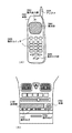
ここで図16(A)は携帯電話であり、本体2601、音声出力部2602、音声入力部2603、表示部2604、操作スイッチ2605、アンテナ2606を含む。本発明の自発光装置は表示部2604に用いることができる。なお、表示部2604は黒色の背景に白色の文字を表示することで携帯電話の消費電力を抑えることができる。
【0201】
また、図16(B)は音響再生装置、具体的には車載用オーディオであり、本体2701、表示部2702、操作スイッチ2703、2704を含む。本発明の自発光装置は表示部2702に用いることができる。また、本実施例では車載用オーディオを示すが、携帯型や家庭用の音響再生装置に用いても良い。なお、表示部2704は黒色の背景に白色の文字を表示することで消費電力を抑えられる。これは携帯型の音響再生装置において特に有効である。
【0202】
以上の様に、本発明の適用範囲は極めて広く、あらゆる分野の電気器具に用いることが可能である。また、本実施例の電気器具は実施例1〜6に示したいずれの構成の自発光装置を用いても良い。
【0203】
〔実施例8〕
本発明において、三重項励起子からの燐光を発光に利用できるEL材料を用いることで、外部発光量子効率を飛躍的に向上させることができる。これにより、EL素子の低消費電力化、長寿命化、および軽量化が可能になる。
ここで、三重項励起子を利用し、外部発光量子効率を向上させた報告を示す。
(T.Tsutsui, C.Adachi, S.Saito, Photochemical Processes in Organized Molecular Systems, ed.K.Honda, (Elsevier Sci.Pub., Tokyo,1991) p.437.)
上記の論文により報告されたEL材料(クマリン色素)の分子式を以下に示す。
【0204】
【化6】
(M.A.Baldo, D.F.O'Brien, Y.You, A.Shoustikov, S.Sibley, M.E.Thompson, S.R.Forrest, Nature 395 (1998) p.151.)
上記の論文により報告されたEL材料(Pt錯体)の分子式を以下に示す。
【0206】
【化7】
(M.A.Baldo, S.Lamansky, P.E.Burrrows, M.E.Thompson, S.R.Forrest, Appl.Phys.Lett.,75 (1999) p.4.)
(T.Tsutsui, M.-J.Yang, M.Yahiro, K.Nakamura, T.Watanabe, T.tsuji, Y.Fukuda, T.Wakimoto, S.Mayaguchi, Jpn.Appl.Phys., 38 (12B) (1999) L1502.)
上記の論文により報告されたEL材料(Ir錯体)の分子式を以下に示す。
【0208】
【化8】
以上のように三重項励起子からの燐光発光を利用できれば原理的には一重項励起子からの蛍光発光を用いる場合より3〜4倍の高い外部発光量子効率の実現が可能となる。なお、本実施例の構成は、実施例1〜実施例7のいずれの構成とも自由に組みあわせて実施することが可能である。
【0210】
【発明の効果】
本発明を実施することで、EL層及びカバー層を同一の塗布方法で形成することができる。これにより、大気解放することなく効率的にEL層、陰極、バリア層及びカバー層を同一のマルチチャンバーで連続的に形成することが可能である。また、バリア層及びカバー層を形成させることでEL層への水分や酸素の進入を防ぎ、EL層の劣化対策に効果的である。また、バリア層及びカバー層を形成することで封止構造が完成するので、通常の封止構造に比べると小型化、軽量化が可能となる。
【図面の簡単な説明】
【図1】 本発明の薄膜形成方法を示す図。
【図2】 画素部の断面構造を示す図。
【図3】 画素部の上面構造及び構成を示す図。
【図4】 自発光装置の作製工程を示す図。
【図5】 自発光装置の作製工程を示す図。
【図6】 自発光装置の作製工程を示す図。
【図7】 画素部のTFTの断面構造を示す図。
【図8】 画素部のTFTの断面構造を示す図。
【図9】 自発光装置の外観を示す図。
【図10】 自発光装置の回路ブロック構成を示す図。
【図11】 アクティブマトリクス型の自発光装置の断面構造を示す図。
【図12】 薄膜形成方法を示す図。
【図13】 パッシブ型の自発光装置の断面構造を示す図。
【図14】 パッシブ型の自発光装置の断面構造を示す図。
【図15】 電気器具の具体例を示す図。
【図16】 電気器具の具体例を示す図。[0001]
BACKGROUND OF THE INVENTION
The present invention relates to a self-luminous device in which an EL element having a structure in which an anode, a cathode, and a light-emitting organic material (hereinafter referred to as organic EL material) from which EL (Electro Luminescence) is sandwiched is formed on an insulator. The present invention also relates to a method for manufacturing an electric appliance having the light-emitting device as a display portion (display display or display monitor). The self-luminous device is also referred to as OLED (Organic Light Emitting Diodes).
[0002]
[Prior art]
In recent years, a display device (self-emitting device) using an EL element as a self-emitting element utilizing the EL phenomenon of a light-emitting organic material has been developed. Since the self-light-emitting device is a self-light-emitting type, it does not require a backlight like a liquid crystal display device, and has a wide viewing angle, and thus is promising as a display unit of an electric appliance.
[0003]
Note that an EL element includes a layer containing an organic compound (hereinafter referred to as an EL layer) from which electroluminescence (luminescence generated by applying an electric field) is obtained, an anode layer, and a cathode layer. Luminescence in an organic compound includes light emission (fluorescence) when returning from the singlet excited state to the ground state and light emission (phosphorescence) when returning from the triplet excited state to the ground state. The present invention can also be applied when light emission is used.
[0004]
There are two types of self-luminous devices, a passive type (simple matrix type) and an active type (active matrix type), both of which are actively developed. In particular, active matrix self-luminous devices are currently attracting attention. In addition, low molecular organic EL materials and high molecular (polymer) organic EL materials have been studied as EL materials that can be said to be the center of EL elements, but they are handled more than low molecular organic EL materials. Polymer-based organic EL materials that are easy to heat and have high heat resistance are attracting attention.
[0005]
Examples of the film formation method for the polymer-based organic EL material include a method of coating by controlling with an electric field and an ink jet method proposed by Seiko Epson Corporation.
[0006]
[Problems to be solved by the invention]
In the present invention, an EL layer and a film made of an organic material (organic resin) formed on the EL element so as to cover the EL element (hereinafter referred to as a cover layer) are formed using the same method. Note that the cover layer is made of an organic material formed on the cathode of the EL element including the anode, the EL layer, and the cathode, and providing this cover layer is effective for stress relaxation of the TFT or EL element. It is. Furthermore, entry of moisture and oxygen into the EL layer can be prevented, and thereby deterioration of the EL layer can be prevented. Furthermore, by forming a film made of an inorganic material (hereinafter referred to as a barrier layer) on the cover layer, moisture and oxygen can be prevented from entering the cover layer or the EL layer.
[0007]
In addition, this invention makes it a subject to process continuously from EL layer to a cathode, a barrier layer, and a cover layer within the same multi-chamber.
[0008]
Another object of the present invention is to form a cover layer at a desired position with good controllability. It is another object of the present invention to provide a self-luminous device using such means and a manufacturing method thereof, and to provide an electric appliance having such a self-luminous device as a display portion.
[0009]
[Means for Solving the Problems]
The multi-chamber used to achieve the above-mentioned problems is a coating chamber for coating and forming an EL layer and a cover layer made of an organic material by an electric field coating method or an inkjet method, and a deposition chamber for forming a cathode by a deposition method. And a film forming apparatus having a sputtering chamber for forming a barrier layer made of silicon nitride or tantalum oxide.
[0010]
In the present invention, when an EL layer is formed by applying a solution in which an EL material is dissolved in a solvent, this solution is provided in the material chamber. In the present specification, this solution is referred to as a coating solution. When the coating liquid becomes mist-like and has electric charge, the electric field applied by the electrode is controlled to form a film at the coating position on the substrate.
[0011]
The cover layer is formed by providing an organic resin liquid for forming an organic resin film in a material chamber and applying the same in the same manner as the EL layer formation.
[0012]
In the present invention, the barrier layer may be formed after the cover layer is formed on the cathode of the EL element, or the cover layer is formed after the barrier layer is formed on the cathode of the EL element. It is good also as a structure.
[0013]
DETAILED DESCRIPTION OF THE INVENTION
Here, an embodiment of the present invention will be described with reference to FIG. As shown in FIG. 1A, the EL layer, the cathode, the barrier layer, and the cover layer can be continuously formed in the same multi-chamber.
[0014]
Note that the barrier layer refers to a passivation film formed of an inorganic material provided to prevent moisture and oxygen from entering the EL layer.
[0015]
First, an EL layer is formed using an electric field coating method or an inkjet method in a coating chamber. Next, a cathode is formed by a vapor deposition method in a vapor deposition chamber, and an inorganic film made of an inorganic material such as diamond-like carbon (DLC) made of silicon nitride, tantalum oxide, aluminum nitride, or carbon is formed on the cathode as a barrier layer by sputtering or It is formed using a plasma CVD method. Finally, the sealing structure of the self-luminous device can be completed by forming a cover layer by an inkjet method in the coating chamber in the same manner as when the EL layer is formed on the barrier layer.
[0016]
As described above, since the same method is used when forming the EL layer and the cover layer, a film can be selectively formed only at a desired position and can be processed in the same chamber. is there.
[0017]
A cross-sectional structure of the laminated film formed in the present invention is shown in FIG. In FIG. 1B, 101 is a glass substrate, and 102 is a current control TFT. Reference numeral 103 denotes a pixel electrode made of a transparent conductive film electrically connected to the current control TFT. On the pixel electrode 103, the EL layer 104 is formed by the method described above. Further, a cathode 105 is formed on the EL layer 104 by an evaporation method.
[0018]
Further, after forming a barrier layer 106 made of an inorganic film such as a DLC film made of silicon nitride, tantalum oxide, or carbon on the cathode 105, a cover layer 107 made of an organic resin film is formed by the same coating method as the EL layer. .
[0019]
FIG. 1C shows an electric field coating method in which the coating liquid is controlled by an electric field when the EL layer and the cover layer 107 are formed. In FIG. 1C,
[0020]
In the case of the present invention, the organic resin liquid is atomized by ultrasonic vibration applied to the
[0021]
The organic resin that has become charged particles is extracted from the
[0022]
Accordingly, a stacked structure as shown in FIG. 1B can be formed in the same multi-chamber, and a sealing structure of the self-luminous device is completed.
[0023]
Note that FIG. 1B shows a case where an EL element is covered, a barrier layer made of an inorganic material is formed, and then a cover layer made of an organic material is formed. After covering and forming a cover layer made of an organic material, a barrier layer made of an inorganic material may be formed.
[0024]
【Example】
[Example 1]
FIG. 2 is a cross-sectional view of a pixel portion of the self-luminous device of the present invention, FIG. 3A is a top view thereof, and FIG. 3B is a circuit configuration thereof. Actually, a plurality of pixels are arranged in stripes to form a pixel portion (image display portion). Note that a cross-sectional view taken along line AA ′ in FIG. 3A corresponds to FIG. Accordingly, since the same reference numerals are used in FIG. 2 and FIG. 3, both drawings should be referred to as appropriate. Further, in the top view of FIG. 3, two pixels are illustrated, but both have the same structure.
[0025]
In FIG. 2, 11 is a substrate, and 12 is an insulating film (hereinafter referred to as a base film) serving as a base. As the
[0026]
The
[0027]
In addition, it is effective to dissipate the heat generated by the TFT by providing the
[0028]
Here, two TFTs are formed in the pixel.
[0029]
However, in the present invention, it is not necessary to limit the switching TFT to an n-channel TFT and the current control TFT to a p-channel TFT. The switching TFT is a p-channel TFT and the current control TFT is an n-channel TFT. Alternatively, both n-channel or p-channel TFTs can be used.
[0030]
The switching
[0031]
As shown in FIG. 3, the
[0032]
The active layer is formed of a semiconductor film including a crystal structure. That is, a single crystal semiconductor film, a polycrystalline semiconductor film, or a microcrystalline semiconductor film may be used. The
[0033]
Further, in the switching
[0034]
Note that it is more preferable to provide an offset region (a region formed of a semiconductor layer having the same composition as the channel formation region to which no gate voltage is applied) between the channel formation region and the LDD region in order to reduce the off-current value. In the case of a multi-gate structure having two or more gate electrodes, a high-concentration impurity region provided between channel formation regions is effective in reducing the off-current value.
[0035]
Next, the
[0036]
As shown in FIG. 2, the drain of the switching TFT is connected to the gate of the
[0037]
The
[0038]
The length (width) of the LDD region formed in the switching
[0039]
Also, as shown in FIG. 3, the wiring including the
[0040]
Further, from the viewpoint of increasing the amount of current that can be passed, the thickness of the active layer (especially the channel formation region) of the
[0041]
Next,
[0042]
On the
[0043]
It is very important to flatten the step due to the TFT by the second
[0044]
[0045]
In this embodiment, a conductive film made of a compound of indium oxide and tin oxide is used as the pixel electrode. Further, a small amount of gallium may be added thereto. Further, a compound of indium oxide and zinc oxide or a compound of zinc oxide and gallium oxide can be used.
[0046]
After the pixel electrode is formed, a
[0047]
Next, the
Although only one pixel is shown here, EL layers corresponding to each color of R (red), G (green), and B (blue) are formed.
[0048]
A polymer material is used as the organic EL material for forming the EL layer. Typical polymer materials include polyparaphenylene vinylene (PPV), polyvinyl carbazole (PVK), and polyfluorene.
[0049]
There are various types of PPV organic EL materials. For example, the following molecular formulas have been announced.
("H. Shenk, H. Becker, O. Gelsen, E. Kluge, W. Kreuder, and H. Spreitzer," Polymers for Light Emitting Diodes ", Euro Display, Proceedings, 1999, p. 33-37")
[0050]
[Chemical 1]
[Chemical 2]
Further, polyphenylvinyl having a molecular formula described in JP-A-10-92576 can also be used. The molecular formula is:
[0053]
[Chemical 3]
[Formula 4]
The PVK organic EL material has the following molecular formula.
[0056]
[Chemical formula 5]
The polymer organic EL material can be applied by dissolving in a solvent in a polymer state, or can be polymerized after being dissolved in a solvent and applied in a monomer state. When applied in the monomer state, a polymer precursor is first formed and polymerized by heating in vacuum to a polymer.
[0058]
As a specific EL layer, cyanopolyphenylene vinylene may be used for an EL layer emitting red light, polyphenylene vinylene may be used for an EL layer emitting green light, and polyphenylene vinylene or polyalkylphenylene may be used for an EL layer emitting blue light. The film thickness may be 30 to 150 nm (preferably 40 to 100 nm).
[0059]
However, the above example is an example of the organic EL material that can be used as the EL layer of the present invention, and it is not absolutely necessary to limit to this. In the present invention, an EL layer is formed by applying a mixture of an organic EL material and a solvent by an electric field application method and volatilizing and removing the solvent. Accordingly, any organic EL material may be used as long as the solvent does not exceed the glass transition temperature of the EL layer when the solvent is volatilized, or a low molecular EL material not described here may be used, or a low molecular material may be used. And a polymer material may be used together.
[0060]
Typical solvents include toluene, xylene, chlorobenzene, dichlorobenzene, anisole, chloroform, dichloromethane, γ-butyllactone, butyl cellosolve, cyclohexane, NMP (N-methyl-2-pyrrolidone), cyclohexanone, dioxane, or THF. (Tetrahydrofuran). Note that a solution in which the above-described EL material is dissolved in the above solvent is referred to as a coating solution in this specification. The viscosity of the coating solution is 1 × 10 -3 ~ 3x10 -2 Pa · s is preferred.
[0061]
First, as shown in FIG. 1C, the coating liquid provided in the
[0062]
In the present invention, first, the red EL layer coating liquid provided in the
[0063]
By performing the above operation, it is possible to form a plurality of pixel columns arranged in stripes in red, green, and blue on the substrate.
[0064]
The
[0065]
Although not used here, a mask may be provided between the
[0066]
Further, when the
[0067]
After the
[0068]
Since the EL layer is vulnerable to heat as described above, it is desirable to form the
[0069]
In the present invention, after the
[0070]
When the
[0071]
Here, it is also possible to add a desiccant or an antioxidant such as barium oxide in the cover layer made of an organic resin film as a countermeasure against moisture or oxygen that causes deterioration of the EL layer.
[0072]
[Example 2]
A method for simultaneously manufacturing TFTs of a pixel portion and a driver circuit portion provided in the periphery thereof in an embodiment of the present invention will be described with reference to FIGS. However, in order to simplify the description, a CMOS circuit, which is a basic circuit, is illustrated with respect to the drive circuit.
[0073]
First, as shown in FIG. 4A, a
[0074]
Next, an amorphous silicon film (not shown) having a thickness of 50 nm is formed on the
[0075]
Then, the amorphous silicon film is crystallized by a known technique to form a crystalline silicon film (also referred to as a polycrystalline silicon film or a polysilicon film) 302. Known crystallization methods include a thermal crystallization method using an electric furnace, a laser annealing crystallization method using laser light, and a lamp annealing crystallization method using infrared light. In this embodiment, crystallization is performed using excimer laser light using XeCl gas.
[0076]
In this embodiment, a pulse oscillation type excimer laser beam processed into a linear shape is used. However, a rectangular shape, a continuous oscillation type argon laser beam, or a continuous oscillation type excimer laser beam may be used. .
[0077]
In this embodiment, a crystalline silicon film is used as an active layer of a TFT, but an amorphous silicon film can also be used. It is also possible to form the active layer of the switching TFT that needs to reduce the off-current with an amorphous silicon film and form the active layer of the current control TFT with a crystalline silicon film. Since the amorphous silicon film has low carrier mobility, it is difficult for an electric current to flow and an off current is difficult to flow. That is, the advantages of both an amorphous silicon film that hardly allows current to flow and a crystalline silicon film that easily allows current to flow can be utilized.
[0078]
Next, as shown in FIG. 4B, a
[0079]
Then, resist
[0080]
In the n-
[0081]
Next, as shown in FIG. 4C, the
[0082]
Note that activation by heat treatment may be used in combination with the activation of the impurity element by the laser beam. When activation by heat treatment is performed, heat treatment at about 450 to 550 ° C. may be performed in consideration of the heat resistance of the substrate.
[0083]
By this step, an end portion of the n-
[0084]
Next, as shown in FIG. 4D, unnecessary portions of the crystalline silicon film are removed, and island-shaped semiconductor films (hereinafter referred to as active layers) 306 to 309 are formed.
[0085]
Next, as shown in FIG. 4E, a
[0086]
Next, a conductive film having a thickness of 200 to 400 nm is formed and patterned to form
[0087]
The gate electrode may be formed of a single-layer conductive film, but it is preferable to form a stacked film of two layers or three layers as necessary. Any known conductive film can be used as the material of the gate electrode. However, a material that can be finely processed as described above, specifically, that can be patterned to a line width of 2 μm or less is preferable.
[0088]
Typically, a film made of an element selected from tantalum (Ta), titanium (Ti), molybdenum (Mo), tungsten (W), chromium (Cr), and silicon (Si), or a nitride film of the element (Typically a tantalum nitride film, a tungsten nitride film, a titanium nitride film), an alloy film (typically, a Mo—W alloy, a Mo—Ta alloy), or a silicide film of the above elements (typical) Specifically, a tungsten silicide film or a titanium silicide film) can be used. Of course, it may be used as a single layer or may be laminated.
[0089]
In this embodiment, a laminated film composed of a tantalum nitride (TaN) film having a thickness of 50 nm and a tantalum (Ta) film having a thickness of 350 nm is used. This may be formed by sputtering. Further, when an inert gas such as Xe or Ne is added as a sputtering gas, peeling of the film due to stress can be prevented.
[0090]
At this time, the
[0091]
Next, as shown in FIG. 5A, an n-type impurity element (phosphorus in this embodiment) is added in a self-aligning manner using the
[0092]
Next, as shown in FIG. 5B, resist
[0093]
In this step, the source region or drain region of the n-channel TFT is formed. However, in the switching TFT, a part of the n-
[0094]
Next, as shown in FIG. 5C, the resist
[0095]
The
[0096]
Next, after removing the resist
[0097]
At this time, it is important to eliminate oxygen in the atmosphere as much as possible. This is because the presence of even a small amount of oxygen oxidizes the exposed surface of the gate electrode, which increases resistance and makes it difficult to make ohmic contact later. Therefore, the oxygen concentration in the treatment atmosphere in the activation step is 1 ppm or less, preferably 0.1 ppm or less.
[0098]
Next, when the activation process is completed, a
[0099]
With such a structure, the wiring resistance of the gate wiring can be extremely reduced, so that an image display region (pixel portion) having a large area can be formed. That is, the pixel structure of this embodiment is extremely effective in realizing a self-luminous device having a screen size of 10 inches or more (or 30 inches or more) diagonally.
[0100]
Next, as shown in FIG. 6A, a first
[0101]
Further, a hydrogenation treatment is performed by performing a heat treatment at 300 to 450 ° C. for 1 to 12 hours in an atmosphere containing 3 to 100% hydrogen. This step is a step in which the dangling bonds of the semiconductor film are terminated with hydrogen by thermally excited hydrogen. As another means for hydrogenation, plasma hydrogenation (using hydrogen generated by plasmatization) may be performed.
[0102]
Note that the hydrogenation treatment may be performed while the first
[0103]
Next, contact holes are formed in the first
[0104]
Next, a
[0105]
Prior to the formation of the silicon nitride oxide film, H 2 , NH Three It is effective to perform plasma treatment using a gas containing isohydrogen. Hydrogen excited by this pretreatment is supplied to the first
[0106]
Next, as shown in FIG. 6B, a second
[0107]
Next, contact holes are formed in the second
[0108]
Next, as shown in FIG. 6C, a
[0109]
Next, the
[0110]
First, the EL layer coating solution provided in the material chamber is atomized by ultrasonic vibration using an ultrasonic vibrator. When this mist-like EL layer coating solution is charged by an electric field applied by a voltage applied to the electrode, it can be drawn out by a lead electrode provided outside the material chamber. The extracted coating liquid for the EL layer can be applied to a desired position on the
[0111]
In the present invention, first, the red EL layer coating solution is drawn out from the material chamber as a mist-like EL layer coating solution by the extraction electrode, accelerated by the acceleration electrode, and then controlled by the control electrode to change the red color on the pixel. An EL layer is formed in the pixel column that emits light. Next, after the substrate is moved in the lateral direction, a green EL layer coating solution is applied from the material chamber to form a pixel row that should emit green light. Further, the substrate is moved in the horizontal direction, and the blue EL layer coating solution is applied from the material chamber to form a pixel row that should emit blue light.
[0112]
As described above, stripe-like EL layers of three colors are formed by sequentially applying pixel rows that emit red, green, and blue light while moving the substrate. Although only one pixel is illustrated in this embodiment, EL layers that emit light of the same color may be formed one by one or at the same time. If necessary, a mask can be provided between the material chamber and the substrate, or an application field of the coating liquid can be controlled by applying an electric field to the mask.
[0113]
In this embodiment, as an EL material, cyanopolyphenylene vinylene is used for an EL layer emitting red light, polyphenylene vinylene is used for an EL layer emitting green light, and polyphenylene vinylene or polyalkylphenylene is used for an EL layer emitting blue light. good. The film thickness may be 30 to 150 nm (preferably 40 to 100 nm).
[0114]
A known material can be used for the
[0115]
In this embodiment, the electric field application method by electric field control is shown, but an ink jet method or a method of applying an EL layer material as charged particles may be used.
[0116]
In addition, although the light emitting layer is applied and formed for each color, when forming an electron injection layer, an electron transport layer, a hole transport layer, a hole injection layer, an electron blocking layer, or a hole element layer, the light emitting layer The same material may be formed at a time using a method such as a spin coating method or a coating method regardless of the material for forming the film.
[0117]
After the
[0118]
Further, a
[0119]
A
[0120]
When the
[0121]
At this time, if a moisture absorbent such as barium oxide or an antioxidant is added to the inside of the organic resin liquid forming the cover layer, it is effective to prevent moisture and oxygen from entering, which is a cause of deterioration of the EL element.
[0122]
In this embodiment, as shown in FIG. 6C, the active layer of the n-
[0123]
The reason why the LDD region is formed only on the drain region side is to prevent the operation speed from being lowered. In addition, the n-
[0124]
By the way, the active matrix substrate of this embodiment can provide extremely high reliability and improve the operating characteristics by arranging TFTs having an optimal structure not only in the pixel portion but also in the drive circuit portion.
[0125]
First, a TFT having a structure that reduces hot carrier injection so as not to decrease the operating speed as much as possible is used as an n-
[0126]
Next, a cross-sectional structure of an n-channel switching TFT as a TFT in the pixel portion will be described with reference to FIG. In addition, the code | symbol used here respond | corresponds with the code | symbol used in FIG.
[0127]
First, the switching TFT shown in FIG. 7 is provided in FIG. 7A so that the
[0128]
On the other hand, these
[0129]
In the present invention, any of the structures shown in FIGS. 7A and 7B may be used as the switching TFT.
[0130]
Next, as a TFT in the pixel portion, FIG. 8 shows a cross-sectional structure diagram of an n-channel type current control TFT. In addition, the code | symbol used here respond | corresponds with the code | symbol used in FIG.
[0131]
In the current control TFT shown in FIG. 8A, an
[0132]
The current control TFT supplies a current for causing the EL element to emit light, and at the same time controls the supply amount to enable gradation display. Therefore, it is necessary to take measures against deterioration by hot carrier injection so that it does not deteriorate even when current is passed.
[0133]
Regarding deterioration due to hot carrier injection, it is known that a structure in which an LDD region overlaps a gate electrode is very effective. Therefore, as shown in FIG. 8A, a structure in which an LDD region is provided in a region overlapping with the
[0134]
Furthermore, in the TFT structure shown in FIG. DS When the voltage is 10 V or more, the structure shown in FIG. DS Is less than 10V, the structure shown in FIG. 8B is preferable.
[0135]
When the
[0136]
Here, the EL module of this embodiment formed up to the cover layer will be described with reference to FIGS.
[0137]
The active matrix self-luminous device of this embodiment includes a
[0138]
Further, the source side of the
[0139]
The
[0140]
Here, FIG. 9B shows a cross-sectional view of FIG. 9A cut along AA ′. 9A and 9B, the same reference numerals are used for the same portions. In some cases, the same reference numerals are used for the same parts as in FIG.
[0141]
As shown in FIG. 9B, a
[0142]
The
[0143]
In this embodiment, the
[0144]
Next, a
[0145]
A protective substrate made of glass, plastic, and ceramic can be provided over the
[0146]
As described above, by providing the
[0147]
FIG. 10 shows an example of a circuit configuration of the self light emitting device shown in FIG. The self-light emitting device of this embodiment includes a source side driver circuit 1001, a gate side driver circuit (A) 1007, a gate side driver circuit (B) 1011, and a pixel portion 1006. Note that in this specification, the drive circuit portion is a generic term including a source side processing circuit and a gate side drive circuit.
[0148]
The source side driver circuit 1001 includes a shift register 1002, a level shifter 1003, a buffer 1004, and a sampling circuit (sample and hold circuit) 1005. The gate side driver circuit (A) 1007 includes a
[0149]
Here, the driving voltages of the
[0150]
As the
[0151]
In addition, the said structure can be easily implement | achieved by manufacturing TFT according to the manufacturing process shown to FIGS. Further, in this embodiment, only the configuration of the pixel portion and the drive circuit portion is shown. However, according to the manufacturing process of this embodiment, a signal dividing circuit, a D / A converter circuit, an operational amplifier circuit, a γ correction circuit, etc. It is considered that logic circuits other than the drive circuit can be formed on the same insulator, and further, a memory portion, a microprocessor, and the like can be formed.
[0152]
Further, the configuration of the present embodiment can be freely combined with the configuration of the first embodiment.
[0153]
Example 3
Here, manufacture of a stacked structure different from that illustrated in FIG. 1B will be described. In FIG. 11, a current control TFT 101 is formed on a substrate 1100, and a pixel electrode 1102 electrically connected to the current control TFT 1101 is formed as shown. An EL layer 1103 is formed over the pixel electrode 1102. In this embodiment, an inkjet method is used. Note that the EL layer coating liquid used in this example may be formed using the same material as that used in Example 1.
[0154]
Next, a cathode 1104 is formed over the EL layer 1103 by vapor deposition. Note that a material with a low work function such as MgAg or Al—Li is preferably used for the cathode. After forming the cathode 1104, a cover layer 1105 made of an organic resin film is uniformly formed on the pixel portion again by an inkjet method. Note that the thickness of the cover layer 1105 to be formed is preferably 10 nm to 300 nm.
[0155]
As a material for forming the cover layer 1105 made of an organic resin, it is preferable to use a material that has high hardness, is difficult to pass a substance such as moisture or oxygen, and has flatness. Specifically, organic resins such as epoxy resin, acrylic resin, polyimide, polyamide, and silicon resin are preferable. Note that the cover layer 1105 can be selectively formed in the pixel portion because an ink jet method is used.
[0156]
FIG. 12 shows a method for forming a
[0157]
The MLChip is an actuator in which a
[0158]
Then, three stainless steel plates (SUS plates) are stacked on this MLCchip to form a
[0159]
The operation principle of the coating device made of this MLChip is the piezoelectric effect of the
[0160]
After forming the cover layer 1105 as shown in FIG. 11, the barrier layer 1106 is formed so as to cover the cover layer 1105 by a sputtering method. In this embodiment, the barrier layer 1106 is formed of a carbon film, specifically, a DLC film (diamond-like carbon). However, the material for forming the barrier layer 1106 is not limited to this, and tantalum oxide, aluminum nitride, silicon nitride, or the like may be used. Note that the barrier layer 1106 is selectively formed using a shadow mask.
[0161]
As described above, by forming the cover layer 1105 and the barrier layer 1106 on the active matrix substrate, entry of moisture and oxygen, which cause deterioration of the EL element, from the outside can be prevented.
[0162]
Example 4
In this embodiment, the case where the present invention is used for a passive type (simple matrix type) self-luminous device will be described. FIG. 13 is used for the description. In FIG. 13, 1301 is a substrate made of plastic, and 1302 is an anode made of a transparent conductive film. In this embodiment, a compound of indium oxide and zinc oxide is formed as the
[0163]
Further, the
[0164]
Next,
[0165]
By implementing this embodiment, pixels of three colors of red, green and blue are formed in a stripe pattern on the substrate. Note that the colors of the pixels are not necessarily three colors, and may be one color or two colors. Further, the color is not limited to red, green, and blue, and other colors capable of coloring such as yellow, orange, and gray may be used.
[0166]
First, a red EL layer coating solution is prepared in the material chamber. This coating solution is drawn out by an electric field applied by an electrode provided outside. The drawn coating liquid for EL layer is controlled by an electric field and reaches a desired pixel portion. Thereby, an EL layer is formed.
[0167]
First, a red EL layer coating solution is applied. Since the coating liquid is controlled by an electric field, the EL layer coating liquid can be selectively applied to a desired position of the pixel portion. In addition, it is good to apply | coat, moving a nozzle in the direction which forms one pixel row | line.
[0168]
Next, after moving the nozzle so that it can be applied to the adjacent pixel row, the green EL layer coating solution is applied. Further, after moving the nozzle to the adjacent pixel row, a blue EL layer coating solution is applied to form a stripe-shaped EL layer made of red, green, and blue in the pixel portion.
[0169]
By repeating the above operation, stripe-like pixels can be formed in the pixel portion as shown in FIG. Note that the light emitting layers of the same color may be formed one by one or at the same time.
[0170]
Here, the EL layer refers to a single-layer structure having only a light-emitting layer, but a layer made of an organic EL material that contributes to light emission, such as a charge injection layer or a charge transport layer, can also be used. The light emitting layer may be a single layer. For example, when a hole injection layer and a light emitting layer are laminated, the laminated film is called an EL layer.
[0171]
At this time, the distance (D) between pixels adjacent to each other in the same color line is desirably 5 times or more (preferably 10 times) or more of the film thickness (t) of the EL layer. This is because a problem of crosstalk may occur between pixels when D <5t. In addition, since a high-definition image cannot be obtained even if the distance (D) is too far, it is preferable that 5t <D <50t (preferably 10t <D <35t).
[0172]
Alternatively, the banks may be formed in stripes in the horizontal direction, and an EL layer that emits red light, an EL layer that emits green light, and an EL layer that emits blue light may be formed horizontally. At this time, the bank is formed along the gate wiring above the gate wiring through the insulating film.
[0173]
Also in this case, the distance (D) between pixels adjacent to each other in the same color line is 5 times or more (preferably 10 times or more) of the film thickness (t) of the EL layer, more preferably 5t <D <50t ( Preferably, 10t <D <35t).
[0174]
As described above, the application position can be controlled by forming the EL layer by controlling the EL layer coating liquid with an electric field.
[0175]
Thereafter, although not shown in FIG. 13, the plurality of cathodes and protective electrodes are arranged in stripes so that the direction perpendicular to the paper surface is the longitudinal direction and perpendicular to the
[0176]
As described above, an EL element is formed over the
[0177]
After the
[0178]
Next, a
[0179]
FIG. 13 shows a passive self-luminous device having a structure in which a
[0180]
In addition, the structure of a present Example can be implemented in combination with any structure of Example 1- Example 3 freely.
[0181]
Example 5
In the present invention, it is effective to use a DLC film (diamond-like carbon) film made of carbon as the barrier layer. However, if the film thickness is too thick, the transmittance decreases, so the film thickness is preferably 50 nm or less (preferably 10 to 20 nm).
[0182]
As a feature of the DLC film, 1550cm -1 1300cm with asymmetric peaks -1 It has a Raman spectral distribution with shoulders. In addition, when measured with a microhardness meter, it exhibits a hardness of 15 to 25 GPa and has excellent chemical resistance. Therefore, it is effective to form such a DLC film on the EL element or on the cover layer on the EL element. In any case, the DLC film may be formed by a method such as sputtering, ECR plasma CVD, high-frequency plasma CVD, or ion beam evaporation.
[0183]
In addition, the structure of a present Example can be implemented in combination freely with any structure of Examples 1-4.
[0184]
Example 6
It is effective to use a silicon substrate (silicon wafer) as a substrate when implementing the present invention to manufacture an active matrix self-luminous device. When a silicon substrate is used as a substrate, a switching element formed in the pixel portion, a current control element, or a drive element formed in the drive circuit portion is manufactured using a MOSFET manufacturing technique used in conventional ICs or LSIs. Can be used.
[0185]
A MOSFET can form a circuit with very small variation as proven in ICs and LSIs, and is particularly effective for an analog-driven active matrix self-luminous device that expresses gradations with current values.
[0186]
Note that since the silicon substrate is light-shielding, it is necessary to have a structure in which light from the EL layer is emitted to the side opposite to the substrate. The self-light-emitting device of this embodiment is similar to that of FIG. 9 in terms of the EL element structure, but differs in that MOSFETs are used instead of TFTs that form the
[0187]
In addition, the structure of a present Example can be implemented in combination with any structure of Example 1- Example 5 freely.
[0188]
Example 7
A self-luminous device formed by implementing the present invention is self-luminous, and therefore has excellent visibility in a bright place as compared with a liquid crystal display device and has a wide viewing angle. Therefore, it can be used as a display portion of various electronic devices. For example, in order to view TV broadcasts on a large screen, the display device of the present invention can be used as a display unit of an EL display (display with a self-luminous device incorporated in a housing) having a diagonal size of 30 inches or more (typically 40 inches or more). A light emitting device may be used.
[0189]
The EL display includes all information display displays such as a personal computer display, a TV broadcast receiving display, and an advertisement display. In addition, the self-luminous device of the present invention can be used as a display portion of various other electronic devices.
[0190]
Such an electronic device of the present invention includes a video camera, a digital camera, a goggle type display (head mounted display), a navigation system, a sound reproduction device (car audio, audio component, etc.), a notebook type personal computer, a game machine, a mobile phone. Information terminal (mobile computer, mobile phone, portable game machine, electronic book, etc.), image playback device equipped with a recording medium (specifically, playback of a recording medium such as a digital video disc (DVD), and display the image) And a device equipped with a display that can be used. In particular, since a portable information terminal that is often viewed from an oblique direction emphasizes the wide viewing angle, it is desirable to use a self-luminous device. Specific examples of these electronic devices are shown in FIGS.
[0191]
FIG. 15A illustrates an EL display which includes a
[0192]
FIG. 15B shows a video camera, which includes a main body 2101, a display portion 2102, an
[0193]
FIG. 15C shows a part (right side) of a head-mounted EL display, which includes a main body 2201, a signal cable 2202, a
[0194]
FIG. 15D shows an image reproducing device (specifically, a DVD reproducing device) provided with a recording medium, which includes a main body 2301, a recording medium (DVD or the like) 2302, an
[0195]
FIG. 15E illustrates a portable (mobile) computer, which includes a
[0196]
FIG. 15F illustrates a personal computer, which includes a main body 2501, a housing 2502, a display portion 2503, a
[0197]
If the emission luminance of the organic EL material is increased in the future, the light including the output image information can be enlarged and projected by a lens or the like and used for a front type or rear type projector.
[0198]
In addition, the electric appliances often display information distributed through electronic communication lines such as the Internet or CATV (cable television), and in particular, opportunities to display moving image information are increasing. Since the response speed of the organic EL material is very high, the self-light-emitting device is preferable for moving image display. However, if the contour between pixels is blurred, the entire moving image is blurred. Therefore, it is extremely effective to use the self-light-emitting device of the present invention for clarifying the contour between pixels as a display unit of an electric appliance.
[0199]
In addition, since the light emitting device consumes power in the light emitting device, it is desirable to display information so that the light emitting portion is minimized. Therefore, when a self-luminous device is used for a display unit mainly including character information, such as a portable information terminal, particularly a mobile phone or a sound reproduction device, the character information is formed by the light-emitting portion with the non-light-emitting portion as the background. It is desirable to drive.
[0200]
Here, FIG. 16A shows a mobile phone, which includes a
[0201]
FIG. 16B shows a sound reproducing device, specifically, For automotive It is audio and includes a
[0202]
As described above, the application range of the present invention is extremely wide and can be used for electric appliances in various fields. Moreover, the self-light-emitting device of any structure shown in Examples 1-6 may be used for the electric appliance of a present Example.
[0203]
Example 8
In the present invention, by using an EL material that can use phosphorescence from triplet excitons for light emission, the external light emission quantum efficiency can be dramatically improved. This makes it possible to reduce the power consumption, extend the life, and reduce the weight of the EL element.
Here, a report of using triplet excitons to improve the external emission quantum efficiency is shown.
(T. Tsutsui, C. Adachi, S. Saito, Photochemical Processes in Organized Molecular Systems, ed. K. Honda, (Elsevier Sci. Pub., Tokyo, 1991) p.437.)
The molecular formula of the EL material (coumarin dye) reported by the above paper is shown below.
[0204]
[Chemical 6]
(MABaldo, DFO'Brien, Y.You, A.Shoustikov, S.Sibley, METhompson, SRForrest, Nature 395 (1998) p.151.)
The molecular formula of the EL material (Pt complex) reported by the above paper is shown below.
[0206]
[Chemical 7]
(MABaldo, S. Lamansky, PEBurrrows, METhompson, SRForrest, Appl.Phys.Lett., 75 (1999) p.4.)
(T.Tsutsui, M.-J.Yang, M.Yahiro, K.Nakamura, T.Watanabe, T.tsuji, Y.Fukuda, T.Wakimoto, S.Mayaguchi, Jpn.Appl.Phys., 38 (12B (1999) L1502.)
The molecular formula of the EL material (Ir complex) reported by the above paper is shown below.
[0208]
[Chemical 8]
As described above, if phosphorescence emission from triplet excitons can be used, in principle, it is possible to realize an external emission quantum efficiency that is 3 to 4 times higher than that in the case of using fluorescence emission from singlet excitons. In addition, the structure of a present Example can be implemented in combination with any structure of Example 1- Example 7 freely.
[0210]
【The invention's effect】
By implementing the present invention, the EL layer and the cover layer can be formed by the same coating method. Thereby, it is possible to efficiently form the EL layer, the cathode, the barrier layer, and the cover layer continuously in the same multi-chamber without releasing to the atmosphere. In addition, the formation of the barrier layer and the cover layer prevents moisture and oxygen from entering the EL layer, and is effective in measures against deterioration of the EL layer. In addition, since the sealing structure is completed by forming the barrier layer and the cover layer, it is possible to reduce the size and weight as compared with a normal sealing structure.
[Brief description of the drawings]
FIG. 1 is a view showing a thin film forming method of the present invention.
FIG. 2 illustrates a cross-sectional structure of a pixel portion.
FIG. 3 is a diagram showing a top structure and a configuration of a pixel portion.
FIGS. 4A and 4B are diagrams illustrating a manufacturing process of a self-luminous device. FIGS.
FIGS. 5A and 5B are diagrams illustrating a manufacturing process of a self-luminous device. FIGS.
6A and 6B illustrate a manufacturing process of a self-luminous device.
FIG. 7 shows a cross-sectional structure of a TFT in a pixel portion.
FIG. 8 shows a cross-sectional structure of a TFT in a pixel portion.
FIG. 9 is a diagram illustrating an appearance of a self-luminous device.
FIG. 10 is a diagram showing a circuit block configuration of a self-luminous device.
FIG. 11 illustrates a cross-sectional structure of an active matrix self-luminous device.
FIG. 12 shows a thin film forming method.
FIG 13 illustrates a cross-sectional structure of a passive self-luminous device.
FIG 14 illustrates a cross-sectional structure of a passive self-luminous device.
FIG. 15 is a diagram showing a specific example of an electric appliance.
FIG. 16 is a diagram showing a specific example of an electric appliance.
Claims (3)
前記EL素子を覆う無機材料からなる膜をCVD法または蒸着法により形成し、
前記無機材料からなる膜を覆う有機材料からなる膜を形成し、
前記EL層及び前記有機材料からなる膜は、第1の電極によって霧状の粒子を帯電させ、第2の電極によって前記霧状の粒子を引き出し、第3の電極によって前記霧状の粒子を飛翔方向に加速させ、第4の電極によって前記霧状の粒子が塗布される位置を制御することにより形成することを特徴とする自発光装置の作製方法。A method for producing a self-luminous device having an EL element comprising an anode, an EL layer and a cathode,
A film made of an inorganic material covering the EL element is formed by a CVD method or a vapor deposition method,
Forming a film made of an organic material covering the film made of the inorganic material;
The film made of the EL layer and the organic material charges the mist-like particles by the first electrode, pulls out the mist-like particles by the second electrode, and flies the mist-like particles by the third electrode. A method for producing a self-luminous device, characterized in that the self-luminous device is formed by accelerating in a direction and controlling a position where the mist-like particles are applied by a fourth electrode .
前記EL素子を覆う有機材料からなる膜を形成し、
前記有機材料からなる膜を覆う無機材料からなる膜をCVD法または蒸着法により形成し、
前記EL層及び前記有機材料からなる膜は、第1の電極によって霧状の粒子を帯電させ、第2の電極によって前記霧状の粒子を引き出し、第3の電極によって前記霧状の粒子を飛翔方向に加速させ、第4の電極によって前記霧状の粒子が塗布される位置を制御することにより形成することを特徴とする自発光装置の作製方法。A method for producing a self-luminous device having an EL element comprising an anode, an EL layer and a cathode,
Forming a film made of an organic material covering the EL element;
A film made of an inorganic material covering the film made of the organic material is formed by a CVD method or a vapor deposition method,
The film made of the EL layer and the organic material charges the mist-like particles by the first electrode, pulls out the mist-like particles by the second electrode, and flies the mist-like particles by the third electrode. A method for producing a self-luminous device, characterized in that the self-luminous device is formed by accelerating in a direction and controlling a position where the mist-like particles are applied by a fourth electrode .
前記EL層、前記陰極、前記無機材料からなる膜及び前記有機材料からなる膜を同一の成膜装置で大気開放することなく連続的に形成することを特徴とする自発光装置の作製方法。In claim 1 or claim 2,
A method for manufacturing a self-luminous device, wherein the EL layer, the cathode, the film made of an inorganic material, and the film made of an organic material are continuously formed by the same film forming apparatus without opening to the atmosphere .
Priority Applications (1)
| Application Number | Priority Date | Filing Date | Title |
|---|---|---|---|
| JP2001087851A JP4618918B2 (en) | 2000-03-27 | 2001-03-26 | Method for manufacturing self-luminous device |
Applications Claiming Priority (3)
| Application Number | Priority Date | Filing Date | Title |
|---|---|---|---|
| JP2000-87355 | 2000-03-27 | ||
| JP2000087355 | 2000-03-27 | ||
| JP2001087851A JP4618918B2 (en) | 2000-03-27 | 2001-03-26 | Method for manufacturing self-luminous device |
Publications (3)
| Publication Number | Publication Date |
|---|---|
| JP2001345174A JP2001345174A (en) | 2001-12-14 |
| JP2001345174A5 JP2001345174A5 (en) | 2008-04-17 |
| JP4618918B2 true JP4618918B2 (en) | 2011-01-26 |
Family
ID=26588483
Family Applications (1)
| Application Number | Title | Priority Date | Filing Date |
|---|---|---|---|
| JP2001087851A Expired - Fee Related JP4618918B2 (en) | 2000-03-27 | 2001-03-26 | Method for manufacturing self-luminous device |
Country Status (1)
| Country | Link |
|---|---|
| JP (1) | JP4618918B2 (en) |
Families Citing this family (11)
| Publication number | Priority date | Publication date | Assignee | Title |
|---|---|---|---|---|
| WO2002099477A1 (en) * | 2001-06-01 | 2002-12-12 | Seiko Epson Corporation | Color filter and electro-optical device |
| JP2003297547A (en) * | 2002-03-28 | 2003-10-17 | Idemitsu Kosan Co Ltd | Organic el display device |
| AU2003254851A1 (en) | 2002-08-07 | 2004-02-25 | Kabushiki Kaisha Toyota Chuo Kenkyusho | Laminate having adherent layer and laminate having protective film |
| JP3729262B2 (en) | 2002-08-29 | 2005-12-21 | セイコーエプソン株式会社 | ELECTROLUMINESCENT DEVICE AND ELECTRONIC DEVICE |
| JP3997888B2 (en) | 2002-10-25 | 2007-10-24 | セイコーエプソン株式会社 | Electro-optical device, method of manufacturing electro-optical device, and electronic apparatus |
| US20040238846A1 (en) * | 2003-05-30 | 2004-12-02 | Georg Wittmann | Organic electronic device |
| JP4561201B2 (en) * | 2003-09-04 | 2010-10-13 | セイコーエプソン株式会社 | Electro-optical device, method of manufacturing electro-optical device, and electronic apparatus |
| JP4702009B2 (en) | 2005-11-22 | 2011-06-15 | セイコーエプソン株式会社 | LIGHT EMITTING DEVICE AND ELECTRONIC DEVICE |
| JP4547441B2 (en) * | 2008-03-31 | 2010-09-22 | パナソニック株式会社 | Organic EL ink composition and method for producing the same |
| US10069110B2 (en) | 2014-12-05 | 2018-09-04 | Sharp Kabushiki Kaisha | Organic EL display device |
| WO2018138823A1 (en) * | 2017-01-26 | 2018-08-02 | シャープ株式会社 | Oled panel, method for manufacturing oled panel, and device for manufacturing oled panel |
Citations (10)
| Publication number | Priority date | Publication date | Assignee | Title |
|---|---|---|---|---|
| JPH1064902A (en) * | 1996-07-12 | 1998-03-06 | Applied Materials Inc | Method for film formation of aluminum material and device therefor |
| WO1998012689A1 (en) * | 1996-09-19 | 1998-03-26 | Seiko Epson Corporation | Matrix type display device and method of production thereof |
| JPH10202153A (en) * | 1997-01-20 | 1998-08-04 | Agency Of Ind Science & Technol | Method and device for producing thin film |
| JPH1154266A (en) * | 1997-07-31 | 1999-02-26 | Seiko Epson Corp | Luminescent display |
| JPH1174073A (en) * | 1997-08-29 | 1999-03-16 | Seiko Epson Corp | Active matrix type display device |
| JPH1187063A (en) * | 1997-09-01 | 1999-03-30 | Seiko Epson Corp | Electroluminescent element |
| JPH1197169A (en) * | 1997-09-17 | 1999-04-09 | Casio Comput Co Ltd | Light emitting element and protection material for it |
| JP2000021222A (en) * | 1998-06-30 | 2000-01-21 | Seiko Epson Corp | Light emitting device and manufacture thereof |
| WO2000008899A1 (en) * | 1998-08-03 | 2000-02-17 | Uniax Corporation | Encapsulation of polymer-based solid state devices with inorganic materials |
| JP2000068050A (en) * | 1998-08-24 | 2000-03-03 | Casio Comput Co Ltd | Electroluminescent element and its manufacture |
-
2001
- 2001-03-26 JP JP2001087851A patent/JP4618918B2/en not_active Expired - Fee Related
Patent Citations (11)
| Publication number | Priority date | Publication date | Assignee | Title |
|---|---|---|---|---|
| JPH1064902A (en) * | 1996-07-12 | 1998-03-06 | Applied Materials Inc | Method for film formation of aluminum material and device therefor |
| WO1998012689A1 (en) * | 1996-09-19 | 1998-03-26 | Seiko Epson Corporation | Matrix type display device and method of production thereof |
| JPH10202153A (en) * | 1997-01-20 | 1998-08-04 | Agency Of Ind Science & Technol | Method and device for producing thin film |
| JPH1154266A (en) * | 1997-07-31 | 1999-02-26 | Seiko Epson Corp | Luminescent display |
| JPH1174073A (en) * | 1997-08-29 | 1999-03-16 | Seiko Epson Corp | Active matrix type display device |
| JPH1187063A (en) * | 1997-09-01 | 1999-03-30 | Seiko Epson Corp | Electroluminescent element |
| JPH1197169A (en) * | 1997-09-17 | 1999-04-09 | Casio Comput Co Ltd | Light emitting element and protection material for it |
| JP2000021222A (en) * | 1998-06-30 | 2000-01-21 | Seiko Epson Corp | Light emitting device and manufacture thereof |
| WO2000008899A1 (en) * | 1998-08-03 | 2000-02-17 | Uniax Corporation | Encapsulation of polymer-based solid state devices with inorganic materials |
| JP2002522884A (en) * | 1998-08-03 | 2002-07-23 | ユニアックス コーポレイション | Encapsulation of polymer-based solid devices with inorganic materials |
| JP2000068050A (en) * | 1998-08-24 | 2000-03-03 | Casio Comput Co Ltd | Electroluminescent element and its manufacture |
Also Published As
| Publication number | Publication date |
|---|---|
| JP2001345174A (en) | 2001-12-14 |
Similar Documents
| Publication | Publication Date | Title |
|---|---|---|
| US6781746B2 (en) | Self-light emitting device and method of manufacturing the same | |
| US6696105B2 (en) | Thin film forming device, thin film forming method, and self-light emitting device | |
| KR100764178B1 (en) | A thin film forming device | |
| KR100733898B1 (en) | Method for manufacturing an electro-optical device | |
| JP4831873B2 (en) | Self-luminous device and manufacturing method thereof | |
| JP4987140B2 (en) | Method for manufacturing self-luminous device | |
| JP4637391B2 (en) | Method for manufacturing light emitting device | |
| JP4574039B2 (en) | Method for manufacturing EL display device | |
| JP4601842B2 (en) | Thin film formation method | |
| JP4618918B2 (en) | Method for manufacturing self-luminous device | |
| JP4265818B2 (en) | Electro-optic device | |
| JP4094437B2 (en) | Method for manufacturing electro-optical device | |
| JP4515349B2 (en) | Electro-optic device | |
| JP2007048758A (en) | Method for manufacturing electrooptical device | |
| JP2007188890A (en) | Manufacturing method of electro-optical device |
Legal Events
| Date | Code | Title | Description |
|---|---|---|---|
| A521 | Request for written amendment filed |
Free format text: JAPANESE INTERMEDIATE CODE: A523 Effective date: 20080228 |
|
| A621 | Written request for application examination |
Free format text: JAPANESE INTERMEDIATE CODE: A621 Effective date: 20080228 |
|
| A977 | Report on retrieval |
Free format text: JAPANESE INTERMEDIATE CODE: A971007 Effective date: 20100809 |
|
| A131 | Notification of reasons for refusal |
Free format text: JAPANESE INTERMEDIATE CODE: A131 Effective date: 20100817 |
|
| A521 | Request for written amendment filed |
Free format text: JAPANESE INTERMEDIATE CODE: A523 Effective date: 20100921 |
|
| TRDD | Decision of grant or rejection written | ||
| A01 | Written decision to grant a patent or to grant a registration (utility model) |
Free format text: JAPANESE INTERMEDIATE CODE: A01 Effective date: 20101019 |
|
| A01 | Written decision to grant a patent or to grant a registration (utility model) |
Free format text: JAPANESE INTERMEDIATE CODE: A01 |
|
| A61 | First payment of annual fees (during grant procedure) |
Free format text: JAPANESE INTERMEDIATE CODE: A61 Effective date: 20101026 |
|
| FPAY | Renewal fee payment (event date is renewal date of database) |
Free format text: PAYMENT UNTIL: 20131105 Year of fee payment: 3 |
|
| R150 | Certificate of patent or registration of utility model |
Free format text: JAPANESE INTERMEDIATE CODE: R150 |
|
| FPAY | Renewal fee payment (event date is renewal date of database) |
Free format text: PAYMENT UNTIL: 20131105 Year of fee payment: 3 |
|
| R250 | Receipt of annual fees |
Free format text: JAPANESE INTERMEDIATE CODE: R250 |
|
| R250 | Receipt of annual fees |
Free format text: JAPANESE INTERMEDIATE CODE: R250 |
|
| R250 | Receipt of annual fees |
Free format text: JAPANESE INTERMEDIATE CODE: R250 |
|
| R250 | Receipt of annual fees |
Free format text: JAPANESE INTERMEDIATE CODE: R250 |
|
| LAPS | Cancellation because of no payment of annual fees |