JP4042548B2 - Electro-optical device and electronic apparatus - Google Patents
Electro-optical device and electronic apparatus Download PDFInfo
- Publication number
- JP4042548B2 JP4042548B2 JP2002348623A JP2002348623A JP4042548B2 JP 4042548 B2 JP4042548 B2 JP 4042548B2 JP 2002348623 A JP2002348623 A JP 2002348623A JP 2002348623 A JP2002348623 A JP 2002348623A JP 4042548 B2 JP4042548 B2 JP 4042548B2
- Authority
- JP
- Japan
- Prior art keywords
- layer
- wiring
- lines
- line
- scanning
- Prior art date
- Legal status (The legal status is an assumption and is not a legal conclusion. Google has not performed a legal analysis and makes no representation as to the accuracy of the status listed.)
- Expired - Fee Related
Links
Images


Classifications
-
- H—ELECTRICITY
- H10—SEMICONDUCTOR DEVICES; ELECTRIC SOLID-STATE DEVICES NOT OTHERWISE PROVIDED FOR
- H10K—ORGANIC ELECTRIC SOLID-STATE DEVICES
- H10K59/00—Integrated devices, or assemblies of multiple devices, comprising at least one organic light-emitting element covered by group H10K50/00
- H10K59/10—OLED displays
- H10K59/12—Active-matrix OLED [AMOLED] displays
- H10K59/131—Interconnections, e.g. wiring lines or terminals
-
- H—ELECTRICITY
- H05—ELECTRIC TECHNIQUES NOT OTHERWISE PROVIDED FOR
- H05B—ELECTRIC HEATING; ELECTRIC LIGHT SOURCES NOT OTHERWISE PROVIDED FOR; CIRCUIT ARRANGEMENTS FOR ELECTRIC LIGHT SOURCES, IN GENERAL
- H05B33/00—Electroluminescent light sources
- H05B33/12—Light sources with substantially two-dimensional radiating surfaces
- H05B33/26—Light sources with substantially two-dimensional radiating surfaces characterised by the composition or arrangement of the conductive material used as an electrode
Description
【0001】
【発明の属する技術分野】
【0002】
本発明は、電気光学装置及び電子機器に関するものである。
【従来の技術】
【0003】
有機EL素子を用いた表示装置の一つに、画素回路毎に有機EL素子を制御する駆動トランジスタを備えたアクティブマトリクス型表示装置がある。
【0004】
アクティブマトリクス型表示装置には、前記各画素回路に接続する複数の走査線と複数のデータ線とが形成されている。また、アクティブマトリクス型表示装置には、前記各駆動トランジスタに駆動電圧を供給する複数の電源線が形成されている。
【0005】
この種の表示装置は、前記走査線、前記データ線及び前記電源線が複数の配線層に形成された多層配線構造を成している(例えば、特許文献1参照)。
【0006】
【特許文献1】
特開平11−024606号公報
【発明が解決しようとする課題】
【0007】
ところで、前記走査線を形成するとき、隣接して形成される走査線同士が不純物等の混入によってショートする場合がある。同様に、前記データ線を形成するとき、隣接して形成されるデータ線同士が不純物等の混入によってショートする場合がある。更に、同様に、前記電源線を形成するとき、隣接して形成される電源線同士が不純物等の混入によってショートする場合がある。また、同じ配線層に複数の配線が形成されている場合は、不純物等の混入によってその配線間同士がショートする場合がある。その結果、表示装置の歩留まりが低下してしまう。
【0008】
また、高精細化にともなって画素回路を高密度に配置させることが望まれているが、このような場合においては、前記した走査線同士、データ線同士及び電源線同士の製造時におけるショートが特に顕著になる。
【0009】
本発明は上記問題点を解消するためになされたものであって、その目的は、隣接する各種配線同士がショートするのを抑制することができる電気光学装置及び電子機器を提供することにある。
【課題を解決するための手段】
【0010】
本発明の一実施形態に係る電気光学装置は、基板と、前記基板の一方の面に順次形成された、素子形成層と、配線層と、EL形成層とを有し、前記素子形成層は複数の画素回路がマトリクス状に配置された素子形成領域を有し、前記配線層は前記素子形成領域に対応した位置に、複数の走査線と、複数のデータ線と、複数の電源線と、が形成された配線形成領域を有し、前記EL形成層は、前記素子形成領域に対応した位置にマトリクス状に配置した複数の電気光学素子を有する電気光学装置であって、前記配線層は、第1の層と、前記第1の層と前記EL形成層との間に配置された第2の層とを有し、前記複数の走査線の互いに隣接する走査線は、前記配線形成領域において、前記第1の層と前記第2の層とに交互に振り分けて形成されていることを特徴とする。
【0011】
また、本発明の一実施形態に係る電気光学装置は、前記複数の走査線の内、前記第2の層に形成された走査線はコンタクトホールを介して、前記複数の画素回路の内、対応する画素回路に電気的に接続していることを特徴とする。
【0012】
また、本発明の一実施形態に係る電気光学装置は、前記複数の走査線と前記複数のデータ線とは、平面視において交差するように形成されており、前記複数の電源線は前記複数のデータ線と同一方向に延在し、かつ前記複数の電源線は、平面視において、前記複数のデータ線の隣り合う2つのデータ線の間に前記複数の電源線の内1つの電源線が配置されるよう形成されており、前記複数のデータ線は前記第1の層に形成され、前記複数の電源線は前記第2の層に形成されていることを特徴とする。
【0013】
また、本発明の参考例に係る電気光学装置は、基板と、前記基板の一方の面に順次形成された、素子形成層と、配線層と、EL形成層とを有し、前記素子形成層は複数の画素回路がマトリクス状に配置された素子形成領域を有し、前記配線層は前記素子形成領域に対応した位置に、複数の走査線と、複数のデータ線と、複数の電源線と、が形成された配線形成領域を有し、前記EL形成層は、前記素子形成領域に対応した位置にマトリクス状に配置した複数の電気光学素子を有する電気光学装置であって、前記配線層は、第1の層と、前記第1の層と前記EL形成層との間に配置された第2の層とを有し、前記複数のデータ線は、前記配線形成領域において、前記第1の層と前記第2の層とに交互に振り分けて形成されていることを特徴とする。
【0014】
また、本発明の参考例に係る電気光学装置は、前記複数のデータ線の内、前記第2の層に形成されたデータ線はコンタクトホールを介して、前記複数の画素回路の内、対応する画素回路に電気的に接続していることを特徴とする。
【0015】
また、本発明の一実施形態に係る電子機器は、上記の電気光学装置を備えることを特徴とする。
【0016】
また、本発明の参考例におけるマトリクス基板は、複数の第1配線を備えたマトリクス基板であって、前記複数の第1配線のうち少なくとも1つの第1配線の少なくとも一部分は、前記複数の第1配線のうち他の第1の配線とは異なる層に形成されている。
【0017】
これによれば、複数の第1配線を異なる配線層に形成することによって、同一層で隣接する第1配線間の配線ピッチを大きくすることができる。従って、第1配線を形成するとき、不純物が混入しても第1配線同士のショートを抑制することができる。
【0018】
このマトリクス基板において、さらに複数の第2配線を備え、前記少なくとも1つの第1配線の少なくとも一部分は、前記複数の第2配線と同一層に形成されていてもよい。
【0019】
これによれば、複数の第1配線と複数の第2配線とを備えたマトリクス基板の前記第1配線間の配線ピッチを大きくすることができる。
【0020】
このマトリクス基板において、前記複数の第1配線と前記複数の第2配線の少なくともいずれか一方の配線を、異なる複数の層に交互に振り分けて形成してもよい。
【0021】
これによれば、第1配線同士及び第2配線同士間の配線ピッチを大きくすることができる。従って、第1配線及び第2配線を形成するとき、不純物が混入しても第1配線同士及び第2配線同士のショートを抑制することができる。
【0022】
このマトリクス基板において、前記複数の第1配線と前記複数の第2配線は互いに直交するように形成されていてもよい。
【0023】
これによれば、第1配線と第2配線が直交するように形成されたマトリクス基板の第1配線または第2配線のそれぞれの配線ピッチを大きくすることができる。
【0024】
このマトリクス基板において、前記複数の第1配線と前記複数の第2配線とが交差するそれぞれの位置に、前記第1配線と前記第2配線とに接続する電子回路を備えてもよい。
【0025】
これによれば、第1配線と第2配線とが交差する位置にマトリクス状に配置された電子回路を備えたアクティブマトリクス基板に形成される第1配線間または第2配線間の配線ピッチを大きくすることができる。
【0026】
また、本発明の参考例におけるマトリクス基板は、複数の走査線と複数のデータ線とを備えたマトリクス基板であって、前記複数の走査線のうち少なくとも1つの走査線の少なくとも一部分は、他の前記走査線とは異なる配線層に形成されている。
【0027】
これによれば、複数の走査線を異なる配線層に形成することによって、隣接する走査線間の配線ピッチを大きくすることができる。従って、走査線を形成するとき、不純物が混入しても走査線同士のショートを抑制することができる。
【0028】
また、本発明参考例におけるマトリクス基板は、複数の走査線と複数のデータ線とを備えたマトリクス基板であって、前記複数のデータ線のうち、少なくとも1つのデータ線の少なくとも一部分は、他の前記データ線とは異なる配線層に形成されている。
【0029】
これによれば、複数のデータ線を異なる配線層に形成することによって、隣接するデータ線間の配線ピッチを大きくすることができる。従って、データ線を形成するとき、不純物が混入してもデータ線同士のショートを抑制することができる。
【0030】
また、本発明の参考例におけるマトリクス基板は、複数の走査線と複数のデータ線と複数の電源線とを備えたマトリクス基板であって、前記複数の電源線のうち少なくとも1つの電源線の少なくとも一部分は、他の前記電源線とは異なる配線層に形成されている。
【0031】
これによれば、複数の電源線を異なる配線層に形成することによって、隣接する電源線間の配線ピッチを大きくすることができる。従って、電源線を形成するとき、不純物が混入しても電源線同士のショートを抑制することができる。
【0032】
このマトリクス基板において、前記複数の走査線と前記複数のデータ線と前記複数の電源線の少なくともいずれかを異なる複数の層に交互に振り分けて形成してもよい。
【0033】
これによれば、複数の走査線、複数のデータ線または複数の電源線のいずれかを異なる配線層に形成することによって、隣接する走査線、データ線または電源線間の配線ピッチを大きくすることができる。
【0034】
このマトリクス基板において、前記複数の走査線と前記複数のデータ線は互いに直交するように形成されていてもよい。
【0035】
これによれば、走査線とデータ線とが直交するように形成されたマトリクス基板の走査線またはデータ線の配線ピッチを大きくすることができる。
【0036】
このマトリクス基板において、前記複数の走査線と前記複数のデータ線とが交差するそれぞれの位置に、前記走査線と前記データ線とに接続する電子回路を備えてもよい。
【0037】
これによれば、走査線とデータ線とが交差する位置にマトリクス状に配置された電子回路を備えたアクティブマトリクス基板に形成される走査線間またはデータ線間の配線ピッチを大きくすることができる。このことによって、前記アクティブマトリクス基板の走査線間またはデータ線間のショートを抑制することができるので、同アクティブマトリクス基板の歩留まりを向上させることができる。
【0038】
また、本発明の参考例に係る電子装置は、複数の第1配線を備えた基板と、前記複数の第1配線を介して供給される信号または電力によって駆動される電子素子とを備えた電子装置において、前記複数の第1配線のうち少なくとも1つの第1配線は、他の前記第1配線とは異なる層に形成されている。
【0039】
これによれば、複数の第1配線を備えた電子装置において、前記複数の第1配線を異なる配線層に形成することによって、隣接する第1配線間の配線ピッチを大きくすることができる。従って、第1配線を形成するとき、不純物が混入しても第1配線同士のショートを抑制することができるので、前記電子装置の歩留まりを向上させることができる。
【0040】
この電子装置において、さらに複数の第2配線を備え、前記少なくとも1つの第1配線の少なくとも一部分は、前記複数の第2の配線と同一層に形成されていてもよい。
【0041】
これによれば、複数の第1配線と複数の第2配線とを備えたマトリクス基板の前記第1配線間の配線ピッチを大きくすることができる。
【0042】
この電子装置において、前記複数の第1配線と前記複数の第2配線の少なくともいずれか一方の配線を、異なる複数の配線層に交互に振り分けて形成していてもよい。
【0043】
これによれば、第1配線同士及び第2配線同士間の配線ピッチを大きくすることができる。従って、第1配線及び第2配線を形成するとき、不純物が混入しても第1配線同士及び第2配線同士のショートを抑制することができる。
【0044】
この電子装置において、前記複数の第1配線と前記複数の第2配線は互いに直交するように形成されていてもよい。
【0045】
これによれば、第1配線と第2配線が直交するように形成されたマトリクス基板の第1配線または第2配線のそれぞれの配線ピッチを大きくすることができる。
【0046】
この電子装置において、前記複数の第1配線と前記複数の第2配線とが交差するそれぞれの位置に前記第1配線と前記第2配線とに接続し、前記電子素子を制御する電子回路を備えてもよい。
【0047】
これによれば、第1配線と第2配線とが交差する位置にマトリクス状に配置された電子回路に各種信号を供給する第1配線間または第2配線間の配線ピッチを大きくすることができる。
【0048】
この電子装置において、前記複数の第1配線は信号線であり、前記複数の第2配線は電源線であってもよい。
【0049】
これによれば、信号線同士または電源線同士の配線ピッチを大きくすることができる。
【0050】
この電子装置において、前記信号線は、前記電子回路を選択する選択信号を出力する選択線であってもよい。
【0051】
これによれば、マトリクス状に配置された複数の電子回路を選択する選択線の配線ピッチを大きくすることができる。
【0052】
この電子装置において、前記信号線は、前記電子回路にデータ信号を出力するデータ線であってもよい。
【0053】
これによれば、マトリクス状に配置された複数の電子回路にデータ信号を出力するデータ線の配線ピッチを大きくすることができる。
【0054】
この電子装置において、前記電子回路は、基板上に形成された素子形成層に形成され、前記複数の配線層は、前記素子形成層の上側に形成してもよい。
【0055】
これによれば、基板上に電子回路が形成された素子形成層を備えるとともに、前記素子形成層の上側に第1配線を形成する複数の配線層を備えた構造をなした電子装置において、前記複数の配線層に形成される第1配線のピッチを大きくすることができる。そして、上記構造をなす電子装置の形成時において、不純物の混入による前記第1配線同士のショートを抑制することができる。従って、上記構造をなす電子装置の歩留まりを向上させることができる。
【0056】
この電子装置において、前記電子素子は、前記複数の配線層の上側に前記電子回路に対応して形成されていてもよい。
【0057】
これによれば、前記複数の配線層の上側に電子素子を設けた電子装置の配線間のショートを抑制することができる。
【0058】
この電子装置において、前記電子素子は、電気光学素子又は電流駆動素子であってもよい。
【0059】
これによれば、電気光学素子又は電流駆動素子を備えた電子装置の配線間のショートを抑制することができる。
【0060】
また、本発明の参考例における電気光学装置は、複数の走査線と、複数のデータ線と、複数の電源線と、複数の電気光学素子とを備えた電気光学装置であって、前記複数の走査線のうち少なくとも1つの走査線の少なくとも一部は、他の前記走査線とは異なる層に形成されている。
【0061】
これによれば、電気光学装置に形成された複数の走査線を異なる配線層に形成することによって、隣接する走査線間の配線ピッチを大きくすることができる。従って、走査線を形成するとき、不純物が混入しても走査線同士のショートを抑制することができる。その結果、前記電気光学装置の歩留まりを向上させることができる。
【0062】
また、本発明の参考例における電気光学装置は、複数の走査線と、複数のデータ線と、複数の電源線と、複数の電気光学素子とを備えた電気光学装置であって、前記複数のデータ線のうち少なくとも1つのデータ線の少なくとも一部は、他の前記データ線とは異なる層に形成されている。
【0063】
これによれば、電気光学装置に形成された複数のデータ線を異なる配線層に形成することによって、隣接するデータ線間の配線ピッチを大きくすることができる。従って、データ線を形成するとき、不純物が混入してもデータ線同士のショートを抑制することができる。その結果、前記電気光学装置の歩留まりを向上させることができる。
【0064】
また、本発明の参考例における電気光学装置は、複数の走査線と、複数のデータ線と、複数の電源線と、複数の電気光学素子とを備えた電気光学装置であって、前記複数の電源線のうち少なくとも1つの電源線の少なくとも一部は、他の前記電源線とは異なる層に形成されている。
【0065】
これによれば、電気光学装置に形成された複数の電源線を異なる配線層に形成することによって、隣接する電源線間の配線ピッチを大きくすることができる。従って、電源線を形成するとき、不純物が混入しても電源線同士のショートを抑制することができる。その結果、前記電気光学装置の歩留まりを向上させることができる。
【0066】
この電気光学装置において、前記複数のデータ線と前記複数の走査線は互いに直交するように形成されてもよい。
【0067】
これによれば、走査線とデータ線とが直交するように形成された電気光学装置の走査線またはデータ線のそれぞれの配線ピッチを大きくすることができる。
【0068】
この電気光学装置において、前記複数のデータ線と前記複数の走査線と前記複数の電源線の少なくともいずれか一つを異なる複数の配線層に交互に振り分けて形成してもよい。
【0069】
これによれば、複数の走査線、複数のデータ線または複数の電源線のいずれかを異なる配線層に形成することによって、隣接する走査線、データ線または電源線間の配線ピッチを大きくすることができる。
【0070】
この電気光学装置において、前記複数の走査線と前記複数のデータ線とが交差するそれぞれの位置に、前記走査線と前記データ線とに接続し、前記電気光学素子を制御する複数の電子回路を備えた。
【0071】
これによれば、走査線とデータ線とが交差する位置にマトリクス状に配置された電子回路を備えたアクティブマトリクス基板に形成される走査線間またはデータ線間の配線ピッチを大きくすることができる。従って、アクティブマトリクス方式の電気光学装置の歩留まりを向上させることができる。
【0072】
この電気光学装置において、前記複数の電子回路は、基板上に形成された素子形成層に形成され、前記複数の配線層は、前記素子形成層の上側に形成してもよい。
【0073】
これによれば、基板上に電子回路が形成された素子形成層を備えるとともに、前記素子形成層の上側に走査線、データ線及び電源線を備えた構造をなした電気光学装置において、前記複数の配線層に形成される走査線、データ線及び電源線の配線ピッチを大きくすることができる。従って、上記構造をなす電子装置の形成時において、不純物の混入による前記走査線同士、データ線同士及び電源線同士のショートを抑制することができる。この結果、上記構造をなす電子装置の歩留まりを向上させることができる。
【0074】
この電気光学装置において、前記複数の電子回路は、前記複数の配線層の上側に、それぞれ前記電子回路に対応して形成された電気光学素子を駆動させる電子回路であってもよい。
【0075】
これによれば、前記複数の配線層の上側に電気光学素子を設けた電気光学装置の走査線同士、データ線同士及び電源線同士のショートを抑制することができる。
【0076】
この電気光学装置において、前記電気光学素子は、EL素子であってもよい。
【0077】
これによれば、EL素子を制御する走査線同士、データ線同士及び電源線同士のショートを抑制することができる。
【0078】
この電気光学装置において、前記EL素子は発光層が有機材料で形成された有機EL素子であってもよい。
【0079】
これによれば、有機EL素子を備えた電気光学装置の歩留まりを向上させることができる。
【0080】
また、本発明の参考例における電子機器は、上記の電子装置を実装した。
【0081】
これによれば、配線ピッチを大きくすることで不純物によるショートを抑制した電子装置を実装した電子機器の歩留まりを向上させることができる。
【0082】
また、本発明の参考例における電子機器は、上記の電気光学装置を実装した。
【0083】
これによれば、配線ピッチを大きくすることで不純物によるショートを抑制した電気光学装置を実装した電子機器の歩留まりを向上させることができる。
【発明の実施の形態】
【0084】
(第1実施形態)
以下、本発明を具体化した第1実施形態を図1〜図5に従って説明する。図1は、有機ELディスプレイの分解斜視図である。図2は、画素回路の回路図である。図3は、配線層及び素子形成層の一部分解斜視図である。
【0085】
尚、本実施形態は、本発明の一態様を示すものであり、この発明を限定するものではなく、本発明の技術思想の範囲内で任意に変更可能である。また、以下に示す各図においては、各層や各部材を図面上で認識可能な程度の大きさとするため、各層や各部材ごとに縮尺を異ならせてある。
【0086】
有機ELディスプレイ10は、図1に示すように、EL形成層11と基板Sとから構成されている。EL形成層11は、その発光層が有機材料で形成された複数の有機EL素子11a(図2参照)がマトリクス状に形成された形成層である。基板Sは、素子形成層12と配線層13とが積層された多層配線構造を成している。また、基板Sは、その素子形成層12に複数の画素回路15がマトリクス状に配置形成されたアクティブマトリクス基板である。
【0087】
詳述すると、素子形成層12は、ガラス基板GS上に形成され、その略中央部には素子形成領域Pが形成されている。素子形成領域Pには前記有機EL素子11aを制御するための複数の画素回路15がマトリクス状に配置形成されている。
【0088】
また、素子形成層12は、前記素子形成領域Pの図中左側部に走査線駆動回路16を備えている。更に、素子形成層12は、素子形成領域Pの図中下側部にデータ線駆動回路17を備えている。データ線駆動回路17はその内部に複数の単一ラインドライバ17aが設けられている(図6参照)。また、素子形成層12は、制御回路18を備えている。制御回路18は走査線駆動回路16及びデータ線駆動回路17と電気的に接続されているとともに、図示しない外部装置に接続されている。
【0089】
そして、前記素子形成領域Pに形成される画素回路15は、図2に示すように、駆動トランジスタQd、スイッチングトランジスタQs及び保持キャパシタCoから構成されている。本実施形態では、駆動トランジスタQdはp型TFTであって、スイッチングトランジスタQsはn型TFTである。
【0090】
駆動トランジスタQdは、そのゲート/ソース間に保持キャパシタCoが接続されている。駆動トランジスタQdのゲートはスイッチングトランジスタQsを介して後記するデータ線Xmに接続されている。そして、スイッチングトランジスタQsは、データ線Xmを介して前記データ線駆動回路17の各単一ラインドライバ17aに電気的に接続されている。また、スイッチングトランジスタQsのゲートは後記する走査線Ynを介して前記走査線駆動回路16に電気的に接続されている。駆動トランジスタQdのソースは、後記する電源線Lkに接続されている。駆動トランジスタQdのドレインは、前記配線層13を貫通して形成される図示しない配線を介して前記有機EL素子11aの陽極に接続されている。尚、本実施形態においては、画素回路15を、図2に示した駆動トランジスタQd、スイッチングトランジスタQs及び保持キャパシタCoで構成したが、これに限定されるものではなく、適宜変更してもよい。
【0091】
配線層13は、前記EL形成層11と前記素子形成層12とを電気的に接続するため各種配線が形成されている。また、配線層13は、前記素子形成層12上に形成された各走査線駆動回路16及びデータ線駆動回路17と前記画素回路15とを電気的に接続するための選択線としての走査線Yn及びデータ線Xmが形成されている。
【0092】
詳述すると、配線層13には、図1に示すように、前記素子形成層12の素子形成領域Pに対応した位置に配線形成領域Zが形成されている。配線形成領域Zには、前記素子形成層12に形成された各画素回路15と走査線駆動回路16とを電気的に接続する複数の走査線Yn(nは自然数)がマトリクス状に配置形成された各画素回路15の行方向に沿って形成されている。また、配線形成領域Zには、前記素子形成層12に形成された各画素回路15とデータ線駆動回路17とを電気的に接続する複数のデータ線Xm(mは自然数)がマトリクス状に配置形成された各画素回路15の列方向に沿って形成されている。つまり、前記複数の走査線Ynと複数の複数のデータ線Xmとは互いに直交するように形成されている。そして、前記複数の走査線Ynと前記複数の複数のデータ線Xmとが直交するそれぞれの位置に各走査線Ynと各データ線Xmとに接続する画素回路15が備えられている。
【0093】
前記走査線Ynは、配線形成領域Zの上端側(素子形成層12に形成されたデータ線駆動回路17が形成されている側と対向する側)から第1の走査線Y1、第2の走査線Y2、第3の走査線Y3、・・・の順に配設されている。そして、第1の走査線Y1は、前記素子形成領域P上のデータ線駆動回路17が形成されている側と対向する側に行方向に沿って形成された画素回路20群に対応している。また、データ線Xmは、配線形成領域Zの左端側(素子形成層12に形成された走査線駆動回路16が形成されている側)から第1のデータ線X1、第2のデータ線X2、第3のデータ線X3、・・・の順に配設されている。そして、第1のデータ線X1は、前記素子形成領域P上の走査線駆動回路16が形成されている側に列方向に沿って形成された画素回路20群に対応している。
【0094】
更に、配線形成領域Zには、前記データ線Xmに平行して複数の電源線Lk(kは自然数)が形成されている。電源線Lkは、配線形成領域Zの左端側から第1の電源線L1、第2の電源線L2、第3の電源線L3、・・・の順に配設されている。また、配線形成領域Zには、前記EL形成層11と前記素子形成層12とを電気的に接続する図示しない各種配線が形成されている。
【0095】
詳しくは、配線層13は、図3に示すように、第1配線層ID1と第2配線層ID2とから構成されている。第1配線層ID1は前記素子形成層12上に形成され、第2配線層ID2は前記第1配線層ID1上に形成されている。
【0096】
第1配線層ID1には、前記データ線Xm、走査線Yn及び電源線Lkのうち、走査線Ynの全てが形成されている。また、第1配線層ID1には、複数のデータ線Xmのうち、第1のデータ線X1、第3のデータ線X3、第5のデータ線X5、・・・が形成されている。第2配線層ID2には、前記データ線Xm、走査線Yn及び電源線Lkのうち、電源線Lkの全てが形成されている。また、第2配線層ID2には、複数のデータ線Xmのうち、第2のデータ線X2、第4のデータ線X4、・・・が形成されている。
【0097】
つまり、互いに隣接するデータ線Xmが第1配線層ID1と第2配線層ID2とに交互に形成されている。そして、第2配線層において、第2のデータ線X2は第1の電源線L1と第2の電源線L2との間に形成され、第4のデータ線X4は第3の電源線L3と第4の電源線L4との間に形成されている。同様に、図示しない第6のデータ線X6、第8のデータ線X8、・・は、それぞれ、対応する各電源線Lkの間に形成されている。そして、前記データ線Xmと前記走査線Ynとの交差部に対応する位置に前記画素回路15が形成されている。
【0098】
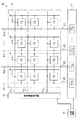
図4は、このように構成された素子形成層12と配線層13との一部上面図である。尚、図4において、実線で示されている部材は、前記第1配線層ID1に構成されたものを示し、2点鎖線で示されている部材は、前記第2配線層ID2に構成されたものを示している。また、破線は素子形成層12に形成された画素回路15の位置を示す。
【0099】
前記第2配線層ID2に形成された第2のデータ線X2、第4のデータ線X4、・・・は、それぞれ対応する画素回路15が形成されている位置に前記第1配線層ID1を貫通して形成されるデータ線用コンタクトホールHXを備えている。そして、前記第2のデータ線X2、第4のデータ線X4、・・・は、それぞれ前記データ線用コンタクトホールHXを介して対応する画素回路15を構成する前記スイッチングトランジスタQsに電気的に接続されている。また、前記第1配線層ID1に形成された第1のデータ線X1、第3のデータ線X3、第5のデータ線X5、・・・は、それぞれ対応する前記画素回路15を構成する前記スイッチングトランジスタQsに直接接続されている。
【0100】
前記第2配線層ID2に形成された電源線Lkは、それぞれ対応する画素回路15が形成されている位置に前記第1配線層ID1を貫通して形成される電源線用コンタクトホールHLを介して、対応する画素回路15を構成する駆動トランジスタQdのソースに電気的に接続されている。そして、前記電源線Lkは、前記電源線用コンタクトホールHLを介して対応する画素回路15を構成する駆動トランジスタQdのソースに電気的に接続されている。
【0101】
また、前記各走査線Ynは、前記走査線駆動回路16と図示しない接続部によって接続されている。同様に、前記各データ線Xmは、データ線駆動回路17と図示しない接続部によって接続されている。
【0102】
図5は、配線層13の一部断面図である。第1配線層ID1には、前記したように、前記スイッチングトランジスタQsのドレインに対応した位置に第1のデータ線X1、第3のデータ線X3、・・・が形成されている。そして、第1配線層ID1に形成された第1の走査線Y1と第1のデータ線X1、第3のデータ線X3、・・・との交差部には絶縁層NCが形成されている。この絶縁層NCは、前記第1の走査線Y1と第1のデータ線X1、第3のデータ線X3、・・・とを電気的に絶縁するためのものである。
【0103】
また、前記第1配線層ID1上に形成された第2配線層ID2には、対応するスイッチングトランジスタQsのドレインに対応した位置に第2のデータ線X2、第4のデータ線X4、・・・が形成されている。第2のデータ線X2は、図5に破線で示すように、前記第1配線層ID1を貫通するデータ線用コンタクトホールHXが形成されている。同様に、第2配線層ID2上に形成された第4のデータ線X4、第6のデータ線X6、・・・についても同第1配線層ID1を貫通するデータ線用コンタクトホールHXがそれぞれ形成されている。そして、第2配線層ID2上に形成された第2のデータ線X2、第4のデータ線X4、・・・はデータ線用コンタクトホールHXを介して対応するスイッチングトランジスタQsのドレインと電気的に接続されている。
【0104】
このように基板S及びその基板Sを備えた有機ELディスプレイ10を構成することによって、前記配線層13に互いに隣接して形成されるデータ線Xmを第1配線層ID1と第2配線層ID2とに交互に振り分けて形成することができる。その結果、データ線Xmの全てを1つの配線層に形成する場合と比較してその配線ピッチを2倍に離間して形成することができる。従って、データ線Xmを形成するとき、隣接して形成されるデータ線Xm同士が不純物等の混入によってショートするのを抑制することができる。その結果、前記基板S及びその基板Sを備えた有機ELディスプレイ10の歩留まりを向上させることができる。
【0105】
次に、このように構成された有機ELディスプレイ10の電気的構成について説明する。
【0106】
図6は、このように構成された有機ELディスプレイ10の電気的構成である。この有機ELディスプレイ10において、前記制御回路18は、図示しない外部装置から供給される画像データに基づいて画像を表示させるための走査制御信号及びデータ制御信号を作成する。そして、制御回路18は、前記走査制御信号を走査線駆動回路16に出力するとともに、前記データ制御信号をデータ線駆動回路17に出力する。
【0107】
そして、データ線駆動回路17はその各単一ラインドライバ17aにて、それぞれ、前記データ線制御信号に基づいてデータ信号VDを生成し、その生成された各データ信号VDを対応するデータ線Xmに出力する。また、走査線駆動回路16は、前記走査制御信号に基づいて前記複数の走査線Ynのうち、1本を選択駆動して1行分の画素回路15群を選択する。そして、選択された画素回路15群に選択信号としての走査信号を出力する。
【0108】
そして、前記走査信号によって選択された走査線Yn上の画素回路15のスイッチングトランジスタQsがオンされる。すると、前記データ線Xmを介して単一ラインドライバ17aから供給されたデータ信号VDが保持キャパシタCoに保持される。
【0109】
このことによって、駆動トランジスタQdの導電率が、前記データ信号VDに応じて制御され、これに応じて有機EL素子11aに供給される駆動電流Ielの電流レベルが制御される。その結果、有機EL素子11aがデータ信号VDに応じて適宜発光動作する。そして、所望の画像が表示される。
【0110】
尚、特許請求の範囲に記載の第1配線、選択線または信号線は、例えば、この実施形態においては、走査線Ynに対応している。また、特許請求の範囲に記載の第2配線は、例えば、この実施形態においては、データ線Xmに対応している。さらに、特許請求の範囲に記載の電子装置または電気光学装置、及び、マトリクス基板は、例えば、この実施形態においては、それぞれ、有機ELディスプレイ10、及び、基板Sに対応している。また、特許請求の範囲に記載の電子素子、電気光学素子または電流駆動素子は、例えば、この実施形態においては、有機EL素子11aに対応している。さらに、特許請求の範囲に記載の信号または電力は、例えば、この実施形態においては、データ信号VDに対応している。また、特許請求の範囲に記載の電子回路は、例えば、この実施形態においては、画素回路15に対応している。
【0111】
前記実施形態の有機ELディスプレイによれば、以下のような特徴を得ることができる。
【0112】
(1)前記実施形態では、複数の画素回路15がマトリクス状に配置形成された素子形成層12と、その素子形成層12上に第1配線層ID1と第2配線層ID2で構成される配線層13とで基板Sを形成した。そして、前記第1配線層ID1及び前記第2配線層ID2に、互いに隣接する前記データ線Xmを交互に形成した。このようにすることによって、1つの配線層にデータ線Xmの全てを形成した基板を使用した場合と比較してデータ線Xmを形成するピッチ2倍にすることができる。
【0113】
従って、データ線Xmを形成するとき、隣接して形成されるデータ線Xm同士が不純物等の混入によってショートするのを抑制することができる。その結果、前記基板S及びその基板Sを備えた有機ELディスプレイ10の歩留まりを向上させることができる。
(第2実施形態)
次に、本発明を具体化した第2実施形態を図7及び図8に従って説明する。尚、本実施形態の有機ELディスプレイ10は、前記第1実施形態におけるデータ線Xmの全てが第1配線層ID1に形成されるとともに、走査線Ynが配線層13を構成する第1配線層ID及び第2配線層ID2に交互に振り分けられて形成されること以外は前記第1実施形態と同じである。従って、本実施形態において、前記第1実施形態と同じ構成部材については符号を等しくし、その詳細な説明を省略する。
【0114】
図7は、本実施形態の配線層13及び素子形成層12で構成される基板Sの一部分解斜視図である。本実施形態におけるデータ線Xmはその全てが第1配線層ID1に形成されている。また、電源線Lkはその全てが第2配線層ID2に形成されている。そして、複数の走査線Ynのうち、第1の走査線Y1、第3の走査線Y3、第5の走査線Y5、・・・は前記第1配線層ID1に形成されるとともに、第2の走査線Y2、第4の走査線Y4、・・・は第2配線層ID2に形成されている。
【0115】
そして、各データ線Xmと各走査線Ynとの交差部に対応する位置に前記画素回路15が前記素子形成層12に形成されている。
【0116】
図8は、このように構成された素子形成層12及び配線層13の一部上面図である。尚、図8において、実線で示されている部材は、前記第1配線層ID1に構成されたものを示し、2点鎖線で示されている部材は、前記第2配線層ID2に構成されたものを示している。また、破線は素子形成層12に形成された画素回路15の位置を示す。
【0117】
前記第2配線層ID2に形成された第2の走査線Y2、第4の走査線Y4、・・・は、図8に示すように、素子形成層12に形成された画素回路15に対応する位置に第1配線層ID1を貫通して形成される走査線用コンタクトホールHYを備えている。走査線用コンタクトホールHYは、画素回路15を構成するスイチングトランジスタQsのゲートに接続されている。このことによって、第2配線層ID2に形成された第2の走査線Y2、第4の走査線Y4、・・・は、対応する前記画素回路15と電気的に接続されている。
【0118】
このように基板S及びその基板Sを備えた有機ELディスプレイ10を構成することによって、配線層13に互いに隣接して形成される走査線Ynを第1配線層ID1と第2配線層ID2に交互に振り分けて形成することができる。その結果、走査線Ynの全てを1つの配線層に形成する場合と比較してその配線ピッチを離間して形成することができる。従って、走査線Ynを形成するとき、隣接して形成される走査線Yn同士が不純物等の混入によってショートするのを抑制することができる。その結果、前記基板S及びその基板Sを備えた有機ELディスプレイ10の歩留まりを向上させることができる。
【0119】
(第3実施形態)
次に、本発明を具体化した第3実施形態を図9及び図10に従って説明する。尚、本実施形態の有機ELディスプレイ10は、前記第1実施形態におけるデータ線Xm及び走査線Ynの全てが第1配線層ID1に形成されるとともに、電源線Lkが配線層13を構成する第1配線層ID及び第2配線層ID2に交互に振り分けて形成される以外は前記第1実施形態と同じである。従って、本実施形態において、前記第1実施形態と同じ構成部材については符号を等しくし、その詳細な説明を省略する。
【0120】
図9は、本実施形態の配線層13及び素子形成層12の一部分解斜視図である。本実施形態における複数のデータ線Xm及び複数の走査線Ynはその全てが第1配線層ID1に形成されている。そして、複数の電源線Lkのうち、第1の電源線L1、第3の電源線L3、第5の電源線L5、・・・は前記第2配線層ID2に形成されるとともに、第2の電源線L2、第4の電源線L4、・・・は第1配線層ID1に形成されている。
【0121】
図10は、素子形成層12及び配線層13の一部上面図である。尚、図10において、実線で示されている部材は、前記第1配線層ID1に構成されたものを示し、2点鎖線で示されている部材は、前記第2配線層ID2に構成されたものを示している。また、破線は素子形成層12に形成された画素回路15の位置を示す。
【0122】
前記第2配線層ID2に形成された第1の電源線L1、第3の電源線L3、・・・は、図10に示すように、第1配線層ID1を貫通して形成された前記電源線用コンタクトホールHLを介して前記素子形成層12に形成された画素回路15を構成する駆動トランジスタQdのソースに電気的に接続されている。また、前記第1配線層ID1に形成された第2の電源線L2、第4の電源線L4、・・・は、駆動トランジスタQdのソースに直接接続されている。
【0123】
このように基板S及びその基板Sを備えた有機ELディスプレイ10を構成することによって、互いに隣接して形成される電源線Lkを第1配線層ID1と第2配線層ID2に交互に形成することができる。その結果、電源線Lkの全てを1つの配線層に形成する場合と比較してその配線ピッチを離間して形成することができる。従って、電源線Lkを形成するとき、隣接して形成される電源線Lk同士が不純物等の混入によってショートするのを抑制することができる。その結果、前記基板S及びその基板Sを備えた有機ELディスプレイ10の歩留まりを向上させることができる。
【0124】
(第4実施形態)
次に、第1〜第3実施形態で説明した電気光学装置としての有機ELディスプレイ10の電子機器の適用について図11に従って説明する。有機ELディスプレイ10は、モバイル型のパーソナルコンピュータ、携帯電話、デジタルカメラ等種々の電子機器に適用できる。
【0125】
図11は、携帯電話の構成を示す斜視図を示す。図11において、携帯電話30は、複数の操作ボタン31、受話口32、送話口33、前記有機ELディスプレイ10を用いた表示ユニット34を備えている。この結果、前記携帯電話30の歩留まりを向上させることができる。
【0126】
尚、発明の実施形態は、上記実施形態に限定されるものではなく、以下のように実施してもよい。
【0127】
○上記第1、第2及び第3実施形態では、電子装置として有機ELディスプレイ10に適用したが、これに限定されるものではなく、他の電子装置に適用してもよい。
【0128】
○上記第1、第2及び第3実施形態では、それぞれ、データ線Xm同士、走査線Yn同士及び電源線Lk同士を第1配線層ID1及び第2配線層ID2に交互に形成することによって各データ線Xm同士、走査線Yn同士及び電源線Lk同士の配線ピッチを離間させた。これを、それぞれ、組み合わせて実施してもよい。
【0129】
例えば、上記第1実施形態では、複数のデータ線Xm、走査線Yn及び電源線Lkのうち、データ線Xmを第1配線層ID1及び第2配線層ID2に交互に形成した。そして、全ての走査線Ynを配線層ID1に形成した。これを、データ線Xmを第1配線層ID1及び第2配線層ID2に交互に形成するとともに、走査線Ynも第1配線層ID1及び第2配線層ID2に交互に形成する。このことによって、第1配線層ID1に形成される走査線Yn同士が、全ての走査線Ynは第1配線層ID1に形成された場合と比べて離間して形成されるので、第1配線層ID1におけるデータ線Xmと走査線Ynとのショートを抑制することができる。
【0130】
○上記第1〜第3実施形態では、有機ELディスプレイ10は、走査線駆動回路16、データ線駆動回路17及び制御回路18のそれぞれが独立した電子部品によって構成されるようにした。これを、走査線駆動回路16、データ線駆動回路17及び制御回路18が1チップの半導体集積回路装置によって構成されていてもよい。又、各走査線駆動回路16、データ線駆動回路17及び制御回路18の全部若しくは一部が一体となった電子部品として構成されていてもよい。このようにすることで、上記第1〜第3実施形態と同様な効果を得ることができる。
【0131】
○上記第1〜第3実施形態では、電子回路として画素回路15に具体化して好適な効果を得たが、例えばLEDやFED等の発光素子のような電流駆動素子を駆動する電子回路に具体化してもよい。
【0132】
○上記第1〜第3実施形態では、電流駆動素子として有機EL素子11aについて具体化したが、無機EL素子に具体化してもよい。つまり、無機EL素子からなる無機ELディスプレイに応用しても良い。
【図面の簡単な説明】
【0133】
【図1】 第1実施形態の有機ELディスプレイの分解斜視図である。
【図2】 画素回路の回路図である。
【図3】 第1実施形態の配線形成層及び素子形成層の一部分解斜視図である。
【図4】 第1実施形態の配線層及び素子形成層の一部上面図である。
【図5】 第1実施形態の第1配線層及び第2配線層の一部断面図である。
【図6】 有機ELディスプレイの電気的構成図である。
【図7】 第2実施形態の配線形成層及び素子形成層の一部分解斜視図である。
【図8】 第2実施形態の配線層及び素子形成層の一部上面図である。
【図9】 第3実施形態の配線形成層及び素子形成層の一部分解斜視図である。
【図10】 第3実施形態の配線層及び素子形成層の一部上面図である。
【図11】 第4実施形態を説明するための携帯電話の構成を示す斜視図である。
【符号の説明】
【0134】
Lk 電源線
S マトリクス基板
VD 信号または電力としてのデータ信号
Xm 第2配線としてのデータ線
Yn 第1配線、選択線または信号線としての走査線
10 電子装置又は電気光学装置としての有機ELディスプレイ
11a 電子素子、電気光学素子または電流駆動素子としての有機EL素子
12 素子形成層
13 配線層
15 電子回路としての画素回路
30 電子機器としての携帯電話[0001]
BACKGROUND OF THE INVENTION
[0002]
The present invention relates to an electro-optical device and an electronic apparatus.
[Prior art]
[0003]
As one of display devices using organic EL elements, there is an active matrix display device provided with a drive transistor for controlling the organic EL element for each pixel circuit.
[0004]
In the active matrix display device, a plurality of scanning lines and a plurality of data lines connected to the pixel circuits are formed. In the active matrix display device, a plurality of power supply lines for supplying a driving voltage to the driving transistors are formed.
[0005]
This type of display device has a multilayer wiring structure in which the scanning lines, the data lines, and the power supply lines are formed in a plurality of wiring layers (see, for example, Patent Document 1).
[0006]
[Patent Document 1]
Japanese Patent Laid-Open No. 11-024606
[Problems to be solved by the invention]
[0007]
By the way, when the scanning lines are formed, adjacent scanning lines may be short-circuited due to impurities or the like. Similarly, when the data lines are formed, adjacent data lines may be short-circuited due to impurities or the like. Further, similarly, when the power supply line is formed, adjacent power supply lines may be short-circuited due to mixing of impurities or the like. In addition, when a plurality of wirings are formed in the same wiring layer, the wirings may be short-circuited due to mixing of impurities or the like. As a result, the yield of the display device is reduced.
[0008]
In addition, it is desired that pixel circuits be arranged with high density as the definition becomes higher. In such a case, a short circuit during the manufacturing of the scan lines, the data lines, and the power supply lines described above may occur. Especially noticeable.
[0009]
SUMMARY An advantage of some aspects of the invention is that it provides an electro-optical device and an electronic apparatus that can suppress a short circuit between various adjacent wirings.
[Means for Solving the Problems]
[0010]
An electro-optical device according to an embodiment of the present invention includes a substrate, an element formation layer, a wiring layer, and an EL formation layer that are sequentially formed on one surface of the substrate, and the element formation layer includes: A plurality of pixel circuits have element formation regions arranged in a matrix, and the wiring layer has a plurality of scanning lines, a plurality of data lines, a plurality of power supply lines at positions corresponding to the element formation regions, The EL formation layer is an electro-optical device having a plurality of electro-optical elements arranged in a matrix at positions corresponding to the element formation region, and the wiring layer includes: A plurality of scanning lines having a first layer and a second layer disposed between the first layer and the EL formation layer; Adjacent scan lines Is formed by alternately distributing the first layer and the second layer in the wiring formation region.
[0011]
In the electro-optical device according to an embodiment of the invention, the scanning line formed in the second layer among the plurality of scanning lines corresponds to the pixel circuit through the contact hole. The pixel circuit is electrically connected to the pixel circuit.
[0012]
In the electro-optical device according to the embodiment of the invention, the plurality of scanning lines and the plurality of data lines are formed so as to intersect in plan view, and the plurality of power supply lines are the plurality of power lines. The plurality of power supply lines extend in the same direction as the data lines, and one of the plurality of power supply lines is arranged between two adjacent data lines of the plurality of data lines in a plan view. The plurality of data lines are formed in the first layer, and the plurality of power supply lines are formed in the second layer.
[0013]
In addition, the present invention Reference example The electro-optical device includes a substrate, an element formation layer, a wiring layer, and an EL formation layer that are sequentially formed on one surface of the substrate, and the element formation layer includes a plurality of pixel circuits in a matrix. Forming a plurality of scanning lines, a plurality of data lines, and a plurality of power supply lines at positions corresponding to the element formation regions. The EL forming layer is an electro-optical device having a plurality of electro-optical elements arranged in a matrix at positions corresponding to the element forming region, and the wiring layer includes the first layer, A second layer disposed between the first layer and the EL formation layer, and the plurality of data lines are arranged in the wiring formation region, the first layer and the second layer. It is characterized by being distributed alternately.
[0014]
In addition, the present invention Reference example In the electro-optical device according to the first aspect, a data line formed in the second layer among the plurality of data lines is electrically connected to a corresponding pixel circuit in the plurality of pixel circuits through a contact hole. It is characterized by that.
[0015]
An electronic apparatus according to an embodiment of the invention includes the above electro-optical device.
[0016]
Further, the matrix substrate in the reference example of the present invention is a matrix substrate including a plurality of first wirings, and at least a part of at least one first wiring among the plurality of first wirings includes the plurality of first wirings. The wiring is formed in a different layer from the other first wiring.
[0017]
According to this, the wiring pitch between the adjacent first wirings in the same layer can be increased by forming the plurality of first wirings in different wiring layers. Therefore, when the first wiring is formed, even if impurities are mixed, a short circuit between the first wirings can be suppressed.
[0018]
The matrix substrate may further include a plurality of second wirings, and at least a part of the at least one first wiring may be formed in the same layer as the plurality of second wirings.
[0019]
According to this, the wiring pitch between the first wirings of the matrix substrate having the plurality of first wirings and the plurality of second wirings can be increased.
[0020]
In this matrix substrate, at least one of the plurality of first wirings and the plurality of second wirings may be alternately distributed and formed on a plurality of different layers.
[0021]
According to this, the wiring pitch between the first wirings and between the second wirings can be increased. Therefore, when the first wiring and the second wiring are formed, even if impurities are mixed, a short circuit between the first wiring and the second wiring can be suppressed.
[0022]
In the matrix substrate, the plurality of first wirings and the plurality of second wirings may be formed to be orthogonal to each other.
[0023]
According to this, each wiring pitch of the 1st wiring or 2nd wiring of a matrix substrate formed so that the 1st wiring and the 2nd wiring may intersect perpendicularly can be enlarged.
[0024]
In this matrix substrate, an electronic circuit connected to the first wiring and the second wiring may be provided at each position where the plurality of first wirings and the plurality of second wirings intersect.
[0025]
According to this, the wiring pitch between the first wirings or between the second wirings formed on the active matrix substrate provided with the electronic circuit arranged in a matrix at the position where the first wiring and the second wiring intersect is increased. can do.
[0026]
Further, the matrix substrate in the reference example of the present invention is a matrix substrate provided with a plurality of scanning lines and a plurality of data lines, and at least a part of at least one scanning line among the plurality of scanning lines includes other It is formed in a wiring layer different from the scanning line.
[0027]
According to this, the wiring pitch between adjacent scanning lines can be increased by forming a plurality of scanning lines in different wiring layers. Therefore, when forming the scanning lines, even if impurities are mixed, a short circuit between the scanning lines can be suppressed.
[0028]
Further, the matrix substrate in the reference example of the present invention is a matrix substrate including a plurality of scanning lines and a plurality of data lines, and at least a part of at least one data line among the plurality of data lines is other It is formed in a wiring layer different from the data line.
[0029]
According to this, the wiring pitch between adjacent data lines can be increased by forming a plurality of data lines in different wiring layers. Therefore, when forming data lines, even if impurities are mixed, short-circuiting between the data lines can be suppressed.
[0030]
Further, the matrix substrate in the reference example of the present invention is a matrix substrate including a plurality of scanning lines, a plurality of data lines, and a plurality of power supply lines, and at least one of at least one of the plurality of power supply lines. A part is formed in a wiring layer different from the other power supply lines.
[0031]
According to this, the wiring pitch between adjacent power supply lines can be increased by forming a plurality of power supply lines in different wiring layers. Accordingly, when the power supply lines are formed, short-circuiting between the power supply lines can be suppressed even if impurities are mixed.
[0032]
In this matrix substrate, at least any one of the plurality of scanning lines, the plurality of data lines, and the plurality of power supply lines may be alternately allocated to a plurality of different layers.
[0033]
According to this, a wiring pitch between adjacent scanning lines, data lines, or power supply lines can be increased by forming any of a plurality of scanning lines, a plurality of data lines, or a plurality of power supply lines in different wiring layers. Can do.
[0034]
In the matrix substrate, the plurality of scanning lines and the plurality of data lines may be formed to be orthogonal to each other.
[0035]
According to this, it is possible to increase the wiring pitch of the scanning lines or data lines of the matrix substrate formed so that the scanning lines and the data lines are orthogonal to each other.
[0036]
In this matrix substrate, an electronic circuit connected to the scanning line and the data line may be provided at each position where the plurality of scanning lines and the plurality of data lines intersect.
[0037]
According to this, it is possible to increase the wiring pitch between the scanning lines or between the data lines formed on the active matrix substrate including the electronic circuits arranged in a matrix at the position where the scanning lines and the data lines intersect. . As a result, a short circuit between scanning lines or data lines of the active matrix substrate can be suppressed, and the yield of the active matrix substrate can be improved.
[0038]
In addition, an electronic device according to a reference example of the present invention includes an electronic device including a substrate including a plurality of first wirings and an electronic element driven by a signal or power supplied via the plurality of first wirings. In the device, at least one first wiring among the plurality of first wirings is formed in a different layer from the other first wirings.
[0039]
According to this, in the electronic device including the plurality of first wirings, the wiring pitch between the adjacent first wirings can be increased by forming the plurality of first wirings in different wiring layers. Therefore, when the first wiring is formed, even if impurities are mixed in, short circuit between the first wirings can be suppressed, so that the yield of the electronic device can be improved.
[0040]
The electronic device may further include a plurality of second wirings, and at least a part of the at least one first wiring may be formed in the same layer as the plurality of second wirings.
[0041]
According to this, the wiring pitch between the first wirings of the matrix substrate having the plurality of first wirings and the plurality of second wirings can be increased.
[0042]
In this electronic device, at least one of the plurality of first wirings and the plurality of second wirings may be alternately allocated to a plurality of different wiring layers.
[0043]
According to this, the wiring pitch between the first wirings and between the second wirings can be increased. Therefore, when the first wiring and the second wiring are formed, even if impurities are mixed, a short circuit between the first wiring and the second wiring can be suppressed.
[0044]
In this electronic device, the plurality of first wirings and the plurality of second wirings may be formed to be orthogonal to each other.
[0045]
According to this, each wiring pitch of the 1st wiring or 2nd wiring of a matrix substrate formed so that the 1st wiring and the 2nd wiring may intersect perpendicularly can be enlarged.
[0046]
The electronic device includes an electronic circuit that controls the electronic element by connecting to the first wiring and the second wiring at each position where the plurality of first wirings and the plurality of second wirings intersect. May be.
[0047]
According to this, it is possible to increase the wiring pitch between the first wirings or between the second wirings for supplying various signals to the electronic circuit arranged in a matrix at the position where the first wiring and the second wiring intersect. .
[0048]
In the electronic device, the plurality of first wirings may be signal lines, and the plurality of second wirings may be power supply lines.
[0049]
According to this, the wiring pitch between the signal lines or between the power supply lines can be increased.
[0050]
In this electronic device, the signal line may be a selection line that outputs a selection signal for selecting the electronic circuit.
[0051]
According to this, the wiring pitch of the selection lines for selecting a plurality of electronic circuits arranged in a matrix can be increased.
[0052]
In this electronic device, the signal line may be a data line that outputs a data signal to the electronic circuit.
[0053]
According to this, the wiring pitch of data lines for outputting data signals to a plurality of electronic circuits arranged in a matrix can be increased.
[0054]
In this electronic device, the electronic circuit may be formed on an element formation layer formed on a substrate, and the plurality of wiring layers may be formed on the element formation layer.
[0055]
According to this, in the electronic device having a structure including the element forming layer in which the electronic circuit is formed on the substrate and including a plurality of wiring layers for forming the first wiring on the element forming layer, The pitch of the first wiring formed in the plurality of wiring layers can be increased. In addition, when the electronic device having the above structure is formed, a short circuit between the first wirings due to the mixing of impurities can be suppressed. Therefore, the yield of the electronic device having the above structure can be improved.
[0056]
In this electronic device, the electronic element may be formed on the upper side of the plurality of wiring layers so as to correspond to the electronic circuit.
[0057]
According to this, it is possible to suppress a short circuit between wires of an electronic device in which an electronic element is provided on the upper side of the plurality of wiring layers.
[0058]
In this electronic device, the electronic element may be an electro-optical element or a current driving element.
[0059]
According to this, it is possible to suppress a short circuit between the wirings of the electronic device including the electro-optical element or the current driving element.
[0060]
An electro-optical device according to a reference example of the present invention is an electro-optical device including a plurality of scanning lines, a plurality of data lines, a plurality of power supply lines, and a plurality of electro-optical elements. At least a part of at least one of the scanning lines is formed in a different layer from the other scanning lines.
[0061]
According to this, the wiring pitch between adjacent scanning lines can be increased by forming the plurality of scanning lines formed in the electro-optical device in different wiring layers. Therefore, when forming the scanning lines, even if impurities are mixed, a short circuit between the scanning lines can be suppressed. As a result, the yield of the electro-optical device can be improved.
[0062]
An electro-optical device according to a reference example of the present invention is an electro-optical device including a plurality of scanning lines, a plurality of data lines, a plurality of power supply lines, and a plurality of electro-optical elements. At least a part of at least one of the data lines is formed in a layer different from the other data lines.
[0063]
According to this, the wiring pitch between adjacent data lines can be increased by forming a plurality of data lines formed in the electro-optical device in different wiring layers. Therefore, when forming data lines, even if impurities are mixed, short-circuiting between the data lines can be suppressed. As a result, the yield of the electro-optical device can be improved.
[0064]
An electro-optical device according to a reference example of the present invention is an electro-optical device including a plurality of scanning lines, a plurality of data lines, a plurality of power supply lines, and a plurality of electro-optical elements. At least a part of at least one of the power supply lines is formed in a different layer from the other power supply lines.
[0065]
According to this, the wiring pitch between adjacent power supply lines can be increased by forming the plurality of power supply lines formed in the electro-optical device in different wiring layers. Accordingly, when the power supply lines are formed, short-circuiting between the power supply lines can be suppressed even if impurities are mixed. As a result, the yield of the electro-optical device can be improved.
[0066]
In the electro-optical device, the plurality of data lines and the plurality of scanning lines may be formed to be orthogonal to each other.
[0067]
According to this, it is possible to increase the wiring pitch of the scanning lines or the data lines of the electro-optical device formed so that the scanning lines and the data lines are orthogonal to each other.
[0068]
In the electro-optical device, at least any one of the plurality of data lines, the plurality of scanning lines, and the plurality of power supply lines may be alternately allocated to a plurality of different wiring layers.
[0069]
According to this, a wiring pitch between adjacent scanning lines, data lines, or power supply lines can be increased by forming any of a plurality of scanning lines, a plurality of data lines, or a plurality of power supply lines in different wiring layers. Can do.
[0070]
In this electro-optical device, a plurality of electronic circuits that control the electro-optical element are connected to the scanning lines and the data lines at positions where the plurality of scanning lines and the plurality of data lines intersect. Prepared.
[0071]
According to this, it is possible to increase the wiring pitch between the scanning lines or between the data lines formed on the active matrix substrate including the electronic circuits arranged in a matrix at the position where the scanning lines and the data lines intersect. . Therefore, the yield of the active matrix electro-optical device can be improved.
[0072]
In the electro-optical device, the plurality of electronic circuits may be formed on an element formation layer formed on a substrate, and the plurality of wiring layers may be formed above the element formation layer.
[0073]
According to this, in the electro-optical device having a structure in which an element forming layer having an electronic circuit formed on a substrate is provided, and a scanning line, a data line, and a power line are provided above the element forming layer, The wiring pitch of the scanning lines, data lines, and power supply lines formed in the wiring layer can be increased. Therefore, when the electronic device having the above structure is formed, a short circuit between the scanning lines, the data lines, and the power supply lines due to mixing of impurities can be suppressed. As a result, the yield of the electronic device having the above structure can be improved.
[0074]
In the electro-optical device, the plurality of electronic circuits may be electronic circuits that drive electro-optical elements formed respectively corresponding to the electronic circuits above the plurality of wiring layers.
[0075]
According to this, it is possible to suppress a short circuit between the scanning lines, the data lines, and the power supply lines of the electro-optical device in which the electro-optical element is provided above the plurality of wiring layers.
[0076]
In this electro-optical device, the electro-optical element may be an EL element.
[0077]
According to this, it is possible to suppress a short circuit between the scanning lines for controlling the EL elements, between the data lines, and between the power supply lines.
[0078]
In this electro-optical device, the EL element may be an organic EL element in which a light emitting layer is formed of an organic material.
[0079]
According to this, the yield of the electro-optical device including the organic EL element can be improved.
[0080]
Moreover, the electronic device in the reference example of the present invention is mounted with the above-described electronic device.
[0081]
According to this, by increasing the wiring pitch, it is possible to improve the yield of the electronic device in which the electronic device in which the short circuit due to impurities is suppressed is mounted.
[0082]
Further, the electronic apparatus in the reference example of the present invention is mounted with the above electro-optical device.
[0083]
According to this, by increasing the wiring pitch, it is possible to improve the yield of the electronic apparatus in which the electro-optical device in which the short circuit due to impurities is suppressed is mounted.
DETAILED DESCRIPTION OF THE INVENTION
[0084]
(First embodiment)
Hereinafter, a first embodiment of the present invention will be described with reference to FIGS. FIG. 1 is an exploded perspective view of an organic EL display. FIG. 2 is a circuit diagram of the pixel circuit. FIG. 3 is a partially exploded perspective view of the wiring layer and the element formation layer.
[0085]
The present embodiment shows one aspect of the present invention, and is not intended to limit the present invention, and can be arbitrarily changed within the scope of the technical idea of the present invention. Moreover, in each figure shown below, in order to make each layer and each member the size which can be recognized on drawing, the scale is varied for each layer and each member.
[0086]
The
[0087]
More specifically, the
[0088]
The
[0089]
As shown in FIG. 2, the
[0090]
The driving transistor Qd has a holding capacitor Co connected between its gate and source. The gate of the driving transistor Qd is connected to a data line Xm described later via the switching transistor Qs. The switching transistor Qs is electrically connected to each
[0091]
The
[0092]
More specifically, as shown in FIG. 1, the
[0093]
The scanning line Yn is the first scanning line Y1, the second scanning from the upper end side of the wiring formation region Z (the side facing the side where the data line driving
[0094]
Further, a plurality of power supply lines Lk (k is a natural number) are formed in the wiring formation region Z in parallel with the data lines Xm. The power supply line Lk is arranged from the left end side of the wiring formation region Z in the order of the first power supply line L1, the second power supply line L2, the third power supply line L3,. In the wiring formation region Z, various wirings (not shown) that electrically connect the
[0095]
Specifically, as shown in FIG. 3, the
[0096]
In the first wiring layer ID1, all of the scanning lines Yn among the data lines Xm, the scanning lines Yn, and the power supply lines Lk are formed. In the first wiring layer ID1, among the plurality of data lines Xm, a first data line X1, a third data line X3, a fifth data line X5,... Are formed. In the second wiring layer ID2, all of the power lines Lk among the data lines Xm, the scanning lines Yn, and the power lines Lk are formed. In the second wiring layer ID2, among the plurality of data lines Xm, a second data line X2, a fourth data line X4,... Are formed.
[0097]
That is, the data lines Xm adjacent to each other are alternately formed in the first wiring layer ID1 and the second wiring layer ID2. In the second wiring layer, the second data line X2 is formed between the first power supply line L1 and the second power supply line L2, and the fourth data line X4 is connected to the third power supply line L3 and the second power supply line L3. 4 power lines L4. Similarly, a sixth data line X6, an eighth data line X8,... (Not shown) are formed between the corresponding power supply lines Lk. The
[0098]
FIG. 4 is a partial top view of the
[0099]
The second data line X2, the fourth data line X4,... Formed in the second wiring layer ID2 pass through the first wiring layer ID1 at the position where the corresponding
[0100]
The power supply line Lk formed in the second wiring layer ID2 is connected to the position where the corresponding
[0101]
Each scanning line Yn is connected to the scanning
[0102]
FIG. 5 is a partial cross-sectional view of the
[0103]
The second wiring layer ID2 formed on the first wiring layer ID1 includes a second data line X2, a fourth data line X4,... At a position corresponding to the drain of the corresponding switching transistor Qs. Is formed. As shown by a broken line in FIG. 5, the second data line X2 has a data line contact hole HX penetrating the first wiring layer ID1. Similarly, for the fourth data line X4, the sixth data line X6,... Formed on the second wiring layer ID2, data line contact holes HX penetrating the first wiring layer ID1 are formed. Has been. The second data line X2, the fourth data line X4,... Formed on the second wiring layer ID2 are electrically connected to the drain of the corresponding switching transistor Qs through the data line contact hole HX. It is connected.
[0104]
By configuring the substrate S and the
[0105]
Next, the electrical configuration of the
[0106]
FIG. 6 shows an electrical configuration of the
[0107]
Then, the data
[0108]
Then, the switching transistor Qs of the
[0109]
Thus, the conductivity of the drive transistor Qd is controlled according to the data signal VD, and the current level of the drive current Iel supplied to the
[0110]
Note that the first wiring, the selection line, or the signal line described in the claims corresponds to, for example, the scanning line Yn in this embodiment. The second wiring recited in the claims corresponds to, for example, the data line Xm in this embodiment. Furthermore, the electronic device or the electro-optical device and the matrix substrate described in the claims correspond to, for example, the
[0111]
According to the organic EL display of the embodiment, the following features can be obtained.
[0112]
(1) In the embodiment, the
[0113]
Therefore, when the data lines Xm are formed, it is possible to prevent the adjacent data lines Xm from being short-circuited due to impurities or the like. As a result, the yield of the substrate S and the
(Second Embodiment)
Next, a second embodiment embodying the present invention will be described with reference to FIGS. In the
[0114]
FIG. 7 is a partially exploded perspective view of the substrate S composed of the
[0115]
The
[0116]
FIG. 8 is a partial top view of the
[0117]
The second scanning line Y2, the fourth scanning line Y4,... Formed in the second wiring layer ID2 correspond to the
[0118]
By configuring the substrate S and the
[0119]
(Third embodiment)
Next, a third embodiment of the present invention will be described with reference to FIGS. In the
[0120]
FIG. 9 is a partially exploded perspective view of the
[0121]
FIG. 10 is a partial top view of the
[0122]
As shown in FIG. 10, the first power supply line L1, the third power supply line L3,... Formed in the second wiring layer ID2 are formed through the first wiring layer ID1. It is electrically connected to the source of the drive transistor Qd constituting the
[0123]
By configuring the substrate S and the
[0124]
(Fourth embodiment)
Next, application of the electronic apparatus of the
[0125]
FIG. 11 is a perspective view showing the configuration of the mobile phone. In FIG. 11, the
[0126]
In addition, embodiment of invention is not limited to the said embodiment, You may implement as follows.
[0127]
In the first, second and third embodiments, the present invention is applied to the
[0128]
In the first, second, and third embodiments, the data lines Xm, the scanning lines Yn, and the power lines Lk are alternately formed in the first wiring layer ID1 and the second wiring layer ID2, respectively. The wiring pitch of the data lines Xm, the scanning lines Yn, and the power supply lines Lk was separated. You may implement this in combination, respectively.
[0129]
For example, in the first embodiment, among the plurality of data lines Xm, scanning lines Yn, and power supply lines Lk, the data lines Xm are alternately formed in the first wiring layer ID1 and the second wiring layer ID2. Then, all the scanning lines Yn are formed in the wiring layer ID1. The data lines Xm are alternately formed in the first wiring layer ID1 and the second wiring layer ID2, and the scanning lines Yn are also alternately formed in the first wiring layer ID1 and the second wiring layer ID2. As a result, the scanning lines Yn formed in the first wiring layer ID1 are formed apart from each other as compared with the case where all the scanning lines Yn are formed in the first wiring layer ID1, so that the first wiring layer A short circuit between the data line Xm and the scanning line Yn in ID1 can be suppressed.
[0130]
In the first to third embodiments, the
[0131]
In the first to third embodiments, the
[0132]
In the first to third embodiments, the
[Brief description of the drawings]
[0133]
FIG. 1 is an exploded perspective view of an organic EL display according to a first embodiment.
FIG. 2 is a circuit diagram of a pixel circuit.
FIG. 3 is a partially exploded perspective view of a wiring formation layer and an element formation layer according to the first embodiment.
FIG. 4 is a partial top view of the wiring layer and the element formation layer of the first embodiment.
FIG. 5 is a partial cross-sectional view of a first wiring layer and a second wiring layer according to the first embodiment.
FIG. 6 is an electrical configuration diagram of an organic EL display.
FIG. 7 is a partially exploded perspective view of a wiring formation layer and an element formation layer according to the second embodiment.
FIG. 8 is a partial top view of a wiring layer and an element formation layer according to a second embodiment.
FIG. 9 is a partially exploded perspective view of a wiring formation layer and an element formation layer according to a third embodiment.
FIG. 10 is a partial top view of a wiring layer and an element formation layer according to a third embodiment.
FIG. 11 is a perspective view showing a configuration of a mobile phone for explaining a fourth embodiment.
[Explanation of symbols]
[0134]
Lk power line
S matrix substrate
VD signal or data signal as power
Xm Data line as second wiring
Yn Scanning line as first wiring, selection line or signal line
10 Organic EL display as an electronic device or electro-optical device
11a Organic EL element as an electronic element, electro-optical element or current drive element
12 Element formation layer
13 Wiring layer
15 Pixel circuit as an electronic circuit
30 Mobile phones as electronic devices
Claims (4)
前記配線層は、第1の層と、前記第1の層と前記EL形成層との間に配置された第2の層とを有し、
前記複数の走査線の互いに隣接する走査線は、前記配線形成領域において、前記第1の層と前記第2の層とに交互に振り分けて形成されていることを特徴とする電気光学装置。An element formation in which a substrate, an element formation layer, a wiring layer, and an EL formation layer, which are sequentially formed on one surface of the substrate, are arranged and a plurality of pixel circuits are arranged in a matrix The wiring layer has a wiring formation region in which a plurality of scanning lines, a plurality of data lines, and a plurality of power supply lines are formed at a position corresponding to the element formation region, and the EL The formation layer is an electro-optical device having a plurality of electro-optical elements arranged in a matrix at positions corresponding to the element formation regions,
The wiring layer includes a first layer, and a second layer disposed between the first layer and the EL formation layer,
The scanning lines adjacent to each other of the plurality of scanning lines are formed by alternately distributing the first layer and the second layer in the wiring formation region.
Priority Applications (5)
| Application Number | Priority Date | Filing Date | Title |
|---|---|---|---|
| JP2002348623A JP4042548B2 (en) | 2002-11-29 | 2002-11-29 | Electro-optical device and electronic apparatus |
| TW092128322A TWI266384B (en) | 2002-11-29 | 2003-10-13 | Matrix substrate, electronic apparatus, electro-optic apparatus, and electronic unit |
| KR1020030071992A KR100559806B1 (en) | 2002-11-29 | 2003-10-16 | Matrix substrate, electronic apparatus, electro-optic apparatus and electronic instrument |
| CNB2003101141117A CN100383608C (en) | 2002-11-29 | 2003-11-05 | Matrix substrate, electronic apparatus, electro-optic apparatus, and electronic unit |
| US10/702,591 US7026754B2 (en) | 2002-11-29 | 2003-11-07 | Matrix substrate having wiring lines formed in different wiring layers |
Applications Claiming Priority (1)
| Application Number | Priority Date | Filing Date | Title |
|---|---|---|---|
| JP2002348623A JP4042548B2 (en) | 2002-11-29 | 2002-11-29 | Electro-optical device and electronic apparatus |
Publications (2)
| Publication Number | Publication Date |
|---|---|
| JP2004184531A JP2004184531A (en) | 2004-07-02 |
| JP4042548B2 true JP4042548B2 (en) | 2008-02-06 |
Family
ID=32588076
Family Applications (1)
| Application Number | Title | Priority Date | Filing Date |
|---|---|---|---|
| JP2002348623A Expired - Fee Related JP4042548B2 (en) | 2002-11-29 | 2002-11-29 | Electro-optical device and electronic apparatus |
Country Status (5)
| Country | Link |
|---|---|
| US (1) | US7026754B2 (en) |
| JP (1) | JP4042548B2 (en) |
| KR (1) | KR100559806B1 (en) |
| CN (1) | CN100383608C (en) |
| TW (1) | TWI266384B (en) |
Families Citing this family (12)
| Publication number | Priority date | Publication date | Assignee | Title |
|---|---|---|---|---|
| JP4686122B2 (en) * | 2003-11-28 | 2011-05-18 | 東芝モバイルディスプレイ株式会社 | Active matrix display device and manufacturing method thereof |
| JP2006066871A (en) * | 2004-07-27 | 2006-03-09 | Seiko Epson Corp | Light emitting device, image forming apparatus, and display device |
| US7351972B2 (en) * | 2004-08-19 | 2008-04-01 | Drs Sensors & Targeting Systems, Inc. | Infrared radiation image having sub-pixelization and detector interdigitation |
| JP2006201217A (en) | 2005-01-18 | 2006-08-03 | Seiko Epson Corp | Wiring substrate, electrooptical apparatus and electronic equipment |
| JP5107546B2 (en) * | 2006-09-15 | 2012-12-26 | グローバル・オーエルイーディー・テクノロジー・リミテッド・ライアビリティ・カンパニー | Display device |
| JP2009169071A (en) | 2008-01-16 | 2009-07-30 | Sony Corp | Display device |
| JP2009288773A (en) * | 2008-04-30 | 2009-12-10 | Sony Corp | Display device |
| KR101888423B1 (en) * | 2011-06-10 | 2018-08-17 | 엘지디스플레이 주식회사 | Flat panel display |
| CN107204352B (en) | 2016-03-16 | 2020-06-16 | 昆山工研院新型平板显示技术中心有限公司 | OLED display panel and manufacturing method thereof |
| US10839752B2 (en) * | 2016-09-21 | 2020-11-17 | Sony Semiconductor Solutions Corporation | Display device and electronic apparatus |
| CN109448566A (en) * | 2018-09-27 | 2019-03-08 | 上海天马微电子有限公司 | A kind of display panel and display device |
| CN110706603A (en) * | 2019-11-19 | 2020-01-17 | 江苏上达电子有限公司 | High-resolution dot-matrix electronic driving method based on flexible packaging substrate |
Family Cites Families (9)
| Publication number | Priority date | Publication date | Assignee | Title |
|---|---|---|---|---|
| FR2605442B1 (en) * | 1986-10-17 | 1988-12-09 | Thomson Csf | ELECTROOPTIC VISUALIZATION SCREEN WITH CONTROL TRANSISTORS AND METHOD FOR PRODUCING THE SAME |
| JP3520396B2 (en) | 1997-07-02 | 2004-04-19 | セイコーエプソン株式会社 | Active matrix substrate and display device |
| JP3830238B2 (en) * | 1997-08-29 | 2006-10-04 | セイコーエプソン株式会社 | Active matrix type device |
| JP4269195B2 (en) | 1998-09-25 | 2009-05-27 | ソニー株式会社 | Light emitting or dimming element and manufacturing method thereof |
| US6709806B2 (en) | 2000-03-31 | 2004-03-23 | Kabushiki Kaisha Toshiba | Method of forming composite member |
| JP3766288B2 (en) | 2000-03-31 | 2006-04-12 | 株式会社東芝 | Composite member manufacturing method and electronic package |
| JP2002196685A (en) * | 2000-12-26 | 2002-07-12 | Sumitomo Chem Co Ltd | Substrate with transparent electrode, method for manufacturing the same and its use |
| JP4318438B2 (en) * | 2002-08-26 | 2009-08-26 | 株式会社ルネサステクノロジ | Nonvolatile semiconductor memory device |
| TWI220775B (en) * | 2003-10-03 | 2004-09-01 | Ind Tech Res Inst | Multi-layered complementary wire structure and manufacturing method thereof |
-
2002
- 2002-11-29 JP JP2002348623A patent/JP4042548B2/en not_active Expired - Fee Related
-
2003
- 2003-10-13 TW TW092128322A patent/TWI266384B/en active
- 2003-10-16 KR KR1020030071992A patent/KR100559806B1/en not_active IP Right Cessation
- 2003-11-05 CN CNB2003101141117A patent/CN100383608C/en not_active Expired - Fee Related
- 2003-11-07 US US10/702,591 patent/US7026754B2/en not_active Expired - Fee Related
Also Published As
| Publication number | Publication date |
|---|---|
| CN100383608C (en) | 2008-04-23 |
| KR100559806B1 (en) | 2006-03-15 |
| KR20040047565A (en) | 2004-06-05 |
| TWI266384B (en) | 2006-11-11 |
| US20040121523A1 (en) | 2004-06-24 |
| JP2004184531A (en) | 2004-07-02 |
| CN1505445A (en) | 2004-06-16 |
| US7026754B2 (en) | 2006-04-11 |
| TW200414797A (en) | 2004-08-01 |
Similar Documents
| Publication | Publication Date | Title |
|---|---|---|
| JP4273809B2 (en) | Electro-optical device and electronic apparatus | |
| JP4165120B2 (en) | Image display device | |
| JP4000515B2 (en) | Electro-optical device, matrix substrate, and electronic apparatus | |
| TWI405165B (en) | Display device | |
| JP4042548B2 (en) | Electro-optical device and electronic apparatus | |
| US20020011976A1 (en) | Display device | |
| JP2008052248A (en) | Display device and flexible member | |
| KR20060053228A (en) | Display and array substrate | |
| JP2007128049A (en) | Display panel | |
| JP2005326704A (en) | Display device | |
| JP4451779B2 (en) | Electroluminescent display device | |
| JP4425264B2 (en) | Scan line drive circuit | |
| JP5245213B2 (en) | LIGHT EMITTING DEVICE AND ELECTRONIC DEVICE | |
| JP2004341513A (en) | Display device | |
| JP4122949B2 (en) | Electro-optical device, active matrix substrate, and electronic apparatus | |
| KR20210018591A (en) | Display device | |
| CN115249731A (en) | Display device and method for manufacturing display device | |
| JP4715197B2 (en) | Electro-optical device and electronic apparatus | |
| JP6597869B2 (en) | Display device and electronic device | |
| JP4963155B2 (en) | Active matrix display device | |
| JP6436209B2 (en) | Display device and electronic device | |
| KR102389384B1 (en) | Foldable display device | |
| JP2004184797A (en) | Electronic device, its manufacturing method and electronic equipment | |
| KR20230159746A (en) | Display device | |
| KR100645535B1 (en) | Organic electro luminescence display device and fabrication method of the same |
Legal Events
| Date | Code | Title | Description |
|---|---|---|---|
| A621 | Written request for application examination |
Free format text: JAPANESE INTERMEDIATE CODE: A621 Effective date: 20050124 |
|
| A977 | Report on retrieval |
Free format text: JAPANESE INTERMEDIATE CODE: A971007 Effective date: 20061117 |
|
| A131 | Notification of reasons for refusal |
Free format text: JAPANESE INTERMEDIATE CODE: A131 Effective date: 20070220 |
|
| RD04 | Notification of resignation of power of attorney |
Free format text: JAPANESE INTERMEDIATE CODE: A7424 Effective date: 20070402 |
|
| A521 | Request for written amendment filed |
Free format text: JAPANESE INTERMEDIATE CODE: A523 Effective date: 20070420 |
|
| A131 | Notification of reasons for refusal |
Free format text: JAPANESE INTERMEDIATE CODE: A131 Effective date: 20070731 |
|
| A521 | Request for written amendment filed |
Free format text: JAPANESE INTERMEDIATE CODE: A523 Effective date: 20070914 |
|
| TRDD | Decision of grant or rejection written | ||
| A01 | Written decision to grant a patent or to grant a registration (utility model) |
Free format text: JAPANESE INTERMEDIATE CODE: A01 Effective date: 20071023 |
|
| A61 | First payment of annual fees (during grant procedure) |
Free format text: JAPANESE INTERMEDIATE CODE: A61 Effective date: 20071105 |
|
| R150 | Certificate of patent or registration of utility model |
Free format text: JAPANESE INTERMEDIATE CODE: R150 |
|
| FPAY | Renewal fee payment (event date is renewal date of database) |
Free format text: PAYMENT UNTIL: 20101122 Year of fee payment: 3 |
|
| FPAY | Renewal fee payment (event date is renewal date of database) |
Free format text: PAYMENT UNTIL: 20101122 Year of fee payment: 3 |
|
| FPAY | Renewal fee payment (event date is renewal date of database) |
Free format text: PAYMENT UNTIL: 20111122 Year of fee payment: 4 |
|
| FPAY | Renewal fee payment (event date is renewal date of database) |
Free format text: PAYMENT UNTIL: 20111122 Year of fee payment: 4 |
|
| FPAY | Renewal fee payment (event date is renewal date of database) |
Free format text: PAYMENT UNTIL: 20121122 Year of fee payment: 5 |
|
| FPAY | Renewal fee payment (event date is renewal date of database) |
Free format text: PAYMENT UNTIL: 20121122 Year of fee payment: 5 |
|
| FPAY | Renewal fee payment (event date is renewal date of database) |
Free format text: PAYMENT UNTIL: 20131122 Year of fee payment: 6 |
|
| LAPS | Cancellation because of no payment of annual fees |