JP3671192B2 - Insulating layered prismatic bump, chip-on-glass product using the bump, and method of manufacturing prismatic bump with insulating layer on the IC chip surface - Google Patents
Insulating layered prismatic bump, chip-on-glass product using the bump, and method of manufacturing prismatic bump with insulating layer on the IC chip surface Download PDFInfo
- Publication number
- JP3671192B2 JP3671192B2 JP2001246861A JP2001246861A JP3671192B2 JP 3671192 B2 JP3671192 B2 JP 3671192B2 JP 2001246861 A JP2001246861 A JP 2001246861A JP 2001246861 A JP2001246861 A JP 2001246861A JP 3671192 B2 JP3671192 B2 JP 3671192B2
- Authority
- JP
- Japan
- Prior art keywords
- insulating layer
- chip
- prismatic
- bump
- prismatic bump
- Prior art date
- Legal status (The legal status is an assumption and is not a legal conclusion. Google has not performed a legal analysis and makes no representation as to the accuracy of the status listed.)
- Expired - Fee Related
Links
Images


Classifications
-
- H—ELECTRICITY
- H01—ELECTRIC ELEMENTS
- H01L—SEMICONDUCTOR DEVICES NOT COVERED BY CLASS H10
- H01L24/00—Arrangements for connecting or disconnecting semiconductor or solid-state bodies; Methods or apparatus related thereto
- H01L24/01—Means for bonding being attached to, or being formed on, the surface to be connected, e.g. chip-to-package, die-attach, "first-level" interconnects; Manufacturing methods related thereto
- H01L24/10—Bump connectors ; Manufacturing methods related thereto
- H01L24/15—Structure, shape, material or disposition of the bump connectors after the connecting process
- H01L24/16—Structure, shape, material or disposition of the bump connectors after the connecting process of an individual bump connector
-
- H—ELECTRICITY
- H01—ELECTRIC ELEMENTS
- H01L—SEMICONDUCTOR DEVICES NOT COVERED BY CLASS H10
- H01L24/00—Arrangements for connecting or disconnecting semiconductor or solid-state bodies; Methods or apparatus related thereto
- H01L24/01—Means for bonding being attached to, or being formed on, the surface to be connected, e.g. chip-to-package, die-attach, "first-level" interconnects; Manufacturing methods related thereto
- H01L24/10—Bump connectors ; Manufacturing methods related thereto
- H01L24/11—Manufacturing methods
-
- H—ELECTRICITY
- H01—ELECTRIC ELEMENTS
- H01L—SEMICONDUCTOR DEVICES NOT COVERED BY CLASS H10
- H01L24/00—Arrangements for connecting or disconnecting semiconductor or solid-state bodies; Methods or apparatus related thereto
- H01L24/01—Means for bonding being attached to, or being formed on, the surface to be connected, e.g. chip-to-package, die-attach, "first-level" interconnects; Manufacturing methods related thereto
- H01L24/10—Bump connectors ; Manufacturing methods related thereto
- H01L24/12—Structure, shape, material or disposition of the bump connectors prior to the connecting process
- H01L24/13—Structure, shape, material or disposition of the bump connectors prior to the connecting process of an individual bump connector
-
- H—ELECTRICITY
- H05—ELECTRIC TECHNIQUES NOT OTHERWISE PROVIDED FOR
- H05K—PRINTED CIRCUITS; CASINGS OR CONSTRUCTIONAL DETAILS OF ELECTRIC APPARATUS; MANUFACTURE OF ASSEMBLAGES OF ELECTRICAL COMPONENTS
- H05K3/00—Apparatus or processes for manufacturing printed circuits
- H05K3/30—Assembling printed circuits with electric components, e.g. with resistor
- H05K3/32—Assembling printed circuits with electric components, e.g. with resistor electrically connecting electric components or wires to printed circuits
- H05K3/321—Assembling printed circuits with electric components, e.g. with resistor electrically connecting electric components or wires to printed circuits by conductive adhesives
- H05K3/323—Assembling printed circuits with electric components, e.g. with resistor electrically connecting electric components or wires to printed circuits by conductive adhesives by applying an anisotropic conductive adhesive layer over an array of pads
-
- H—ELECTRICITY
- H01—ELECTRIC ELEMENTS
- H01L—SEMICONDUCTOR DEVICES NOT COVERED BY CLASS H10
- H01L2224/00—Indexing scheme for arrangements for connecting or disconnecting semiconductor or solid-state bodies and methods related thereto as covered by H01L24/00
- H01L2224/01—Means for bonding being attached to, or being formed on, the surface to be connected, e.g. chip-to-package, die-attach, "first-level" interconnects; Manufacturing methods related thereto
- H01L2224/02—Bonding areas; Manufacturing methods related thereto
- H01L2224/04—Structure, shape, material or disposition of the bonding areas prior to the connecting process
- H01L2224/05—Structure, shape, material or disposition of the bonding areas prior to the connecting process of an individual bonding area
- H01L2224/0554—External layer
- H01L2224/05573—Single external layer
-
- H—ELECTRICITY
- H01—ELECTRIC ELEMENTS
- H01L—SEMICONDUCTOR DEVICES NOT COVERED BY CLASS H10
- H01L2224/00—Indexing scheme for arrangements for connecting or disconnecting semiconductor or solid-state bodies and methods related thereto as covered by H01L24/00
- H01L2224/01—Means for bonding being attached to, or being formed on, the surface to be connected, e.g. chip-to-package, die-attach, "first-level" interconnects; Manufacturing methods related thereto
- H01L2224/10—Bump connectors; Manufacturing methods related thereto
- H01L2224/1012—Auxiliary members for bump connectors, e.g. spacers
- H01L2224/10122—Auxiliary members for bump connectors, e.g. spacers being formed on the semiconductor or solid-state body to be connected
- H01L2224/10125—Reinforcing structures
- H01L2224/10126—Bump collar
-
- H—ELECTRICITY
- H01—ELECTRIC ELEMENTS
- H01L—SEMICONDUCTOR DEVICES NOT COVERED BY CLASS H10
- H01L2224/00—Indexing scheme for arrangements for connecting or disconnecting semiconductor or solid-state bodies and methods related thereto as covered by H01L24/00
- H01L2224/01—Means for bonding being attached to, or being formed on, the surface to be connected, e.g. chip-to-package, die-attach, "first-level" interconnects; Manufacturing methods related thereto
- H01L2224/10—Bump connectors; Manufacturing methods related thereto
- H01L2224/11—Manufacturing methods
- H01L2224/1147—Manufacturing methods using a lift-off mask
-
- H—ELECTRICITY
- H01—ELECTRIC ELEMENTS
- H01L—SEMICONDUCTOR DEVICES NOT COVERED BY CLASS H10
- H01L2224/00—Indexing scheme for arrangements for connecting or disconnecting semiconductor or solid-state bodies and methods related thereto as covered by H01L24/00
- H01L2224/01—Means for bonding being attached to, or being formed on, the surface to be connected, e.g. chip-to-package, die-attach, "first-level" interconnects; Manufacturing methods related thereto
- H01L2224/10—Bump connectors; Manufacturing methods related thereto
- H01L2224/11—Manufacturing methods
- H01L2224/118—Post-treatment of the bump connector
- H01L2224/1182—Applying permanent coating, e.g. in-situ coating
-
- H—ELECTRICITY
- H01—ELECTRIC ELEMENTS
- H01L—SEMICONDUCTOR DEVICES NOT COVERED BY CLASS H10
- H01L2224/00—Indexing scheme for arrangements for connecting or disconnecting semiconductor or solid-state bodies and methods related thereto as covered by H01L24/00
- H01L2224/01—Means for bonding being attached to, or being formed on, the surface to be connected, e.g. chip-to-package, die-attach, "first-level" interconnects; Manufacturing methods related thereto
- H01L2224/10—Bump connectors; Manufacturing methods related thereto
- H01L2224/11—Manufacturing methods
- H01L2224/118—Post-treatment of the bump connector
- H01L2224/1183—Reworking, e.g. shaping
- H01L2224/11831—Reworking, e.g. shaping involving a chemical process, e.g. etching the bump connector
-
- H—ELECTRICITY
- H01—ELECTRIC ELEMENTS
- H01L—SEMICONDUCTOR DEVICES NOT COVERED BY CLASS H10
- H01L2224/00—Indexing scheme for arrangements for connecting or disconnecting semiconductor or solid-state bodies and methods related thereto as covered by H01L24/00
- H01L2224/01—Means for bonding being attached to, or being formed on, the surface to be connected, e.g. chip-to-package, die-attach, "first-level" interconnects; Manufacturing methods related thereto
- H01L2224/10—Bump connectors; Manufacturing methods related thereto
- H01L2224/11—Manufacturing methods
- H01L2224/119—Methods of manufacturing bump connectors involving a specific sequence of method steps
- H01L2224/11901—Methods of manufacturing bump connectors involving a specific sequence of method steps with repetition of the same manufacturing step
- H01L2224/11902—Multiple masking steps
-
- H—ELECTRICITY
- H01—ELECTRIC ELEMENTS
- H01L—SEMICONDUCTOR DEVICES NOT COVERED BY CLASS H10
- H01L2224/00—Indexing scheme for arrangements for connecting or disconnecting semiconductor or solid-state bodies and methods related thereto as covered by H01L24/00
- H01L2224/01—Means for bonding being attached to, or being formed on, the surface to be connected, e.g. chip-to-package, die-attach, "first-level" interconnects; Manufacturing methods related thereto
- H01L2224/10—Bump connectors; Manufacturing methods related thereto
- H01L2224/12—Structure, shape, material or disposition of the bump connectors prior to the connecting process
- H01L2224/13—Structure, shape, material or disposition of the bump connectors prior to the connecting process of an individual bump connector
- H01L2224/13001—Core members of the bump connector
- H01L2224/1301—Shape
- H01L2224/13016—Shape in side view
-
- H—ELECTRICITY
- H01—ELECTRIC ELEMENTS
- H01L—SEMICONDUCTOR DEVICES NOT COVERED BY CLASS H10
- H01L2224/00—Indexing scheme for arrangements for connecting or disconnecting semiconductor or solid-state bodies and methods related thereto as covered by H01L24/00
- H01L2224/01—Means for bonding being attached to, or being formed on, the surface to be connected, e.g. chip-to-package, die-attach, "first-level" interconnects; Manufacturing methods related thereto
- H01L2224/10—Bump connectors; Manufacturing methods related thereto
- H01L2224/12—Structure, shape, material or disposition of the bump connectors prior to the connecting process
- H01L2224/13—Structure, shape, material or disposition of the bump connectors prior to the connecting process of an individual bump connector
- H01L2224/13001—Core members of the bump connector
- H01L2224/13099—Material
- H01L2224/131—Material with a principal constituent of the material being a metal or a metalloid, e.g. boron [B], silicon [Si], germanium [Ge], arsenic [As], antimony [Sb], tellurium [Te] and polonium [Po], and alloys thereof
-
- H—ELECTRICITY
- H01—ELECTRIC ELEMENTS
- H01L—SEMICONDUCTOR DEVICES NOT COVERED BY CLASS H10
- H01L2224/00—Indexing scheme for arrangements for connecting or disconnecting semiconductor or solid-state bodies and methods related thereto as covered by H01L24/00
- H01L2224/01—Means for bonding being attached to, or being formed on, the surface to be connected, e.g. chip-to-package, die-attach, "first-level" interconnects; Manufacturing methods related thereto
- H01L2224/10—Bump connectors; Manufacturing methods related thereto
- H01L2224/12—Structure, shape, material or disposition of the bump connectors prior to the connecting process
- H01L2224/13—Structure, shape, material or disposition of the bump connectors prior to the connecting process of an individual bump connector
- H01L2224/1354—Coating
- H01L2224/1356—Disposition
- H01L2224/13563—Only on parts of the surface of the core, i.e. partial coating
- H01L2224/13565—Only outside the bonding interface of the bump connector
-
- H—ELECTRICITY
- H01—ELECTRIC ELEMENTS
- H01L—SEMICONDUCTOR DEVICES NOT COVERED BY CLASS H10
- H01L2224/00—Indexing scheme for arrangements for connecting or disconnecting semiconductor or solid-state bodies and methods related thereto as covered by H01L24/00
- H01L2224/01—Means for bonding being attached to, or being formed on, the surface to be connected, e.g. chip-to-package, die-attach, "first-level" interconnects; Manufacturing methods related thereto
- H01L2224/10—Bump connectors; Manufacturing methods related thereto
- H01L2224/12—Structure, shape, material or disposition of the bump connectors prior to the connecting process
- H01L2224/13—Structure, shape, material or disposition of the bump connectors prior to the connecting process of an individual bump connector
- H01L2224/1354—Coating
- H01L2224/13599—Material
- H01L2224/136—Material with a principal constituent of the material being a metal or a metalloid, e.g. boron [B], silicon [Si], germanium [Ge], arsenic [As], antimony [Sb], tellurium [Te] and polonium [Po], and alloys thereof
-
- H—ELECTRICITY
- H01—ELECTRIC ELEMENTS
- H01L—SEMICONDUCTOR DEVICES NOT COVERED BY CLASS H10
- H01L2224/00—Indexing scheme for arrangements for connecting or disconnecting semiconductor or solid-state bodies and methods related thereto as covered by H01L24/00
- H01L2224/01—Means for bonding being attached to, or being formed on, the surface to be connected, e.g. chip-to-package, die-attach, "first-level" interconnects; Manufacturing methods related thereto
- H01L2224/26—Layer connectors, e.g. plate connectors, solder or adhesive layers; Manufacturing methods related thereto
- H01L2224/28—Structure, shape, material or disposition of the layer connectors prior to the connecting process
- H01L2224/29—Structure, shape, material or disposition of the layer connectors prior to the connecting process of an individual layer connector
- H01L2224/29001—Core members of the layer connector
- H01L2224/29099—Material
- H01L2224/29198—Material with a principal constituent of the material being a combination of two or more materials in the form of a matrix with a filler, i.e. being a hybrid material, e.g. segmented structures, foams
- H01L2224/29199—Material of the matrix
- H01L2224/2929—Material of the matrix with a principal constituent of the material being a polymer, e.g. polyester, phenolic based polymer, epoxy
-
- H—ELECTRICITY
- H01—ELECTRIC ELEMENTS
- H01L—SEMICONDUCTOR DEVICES NOT COVERED BY CLASS H10
- H01L2224/00—Indexing scheme for arrangements for connecting or disconnecting semiconductor or solid-state bodies and methods related thereto as covered by H01L24/00
- H01L2224/01—Means for bonding being attached to, or being formed on, the surface to be connected, e.g. chip-to-package, die-attach, "first-level" interconnects; Manufacturing methods related thereto
- H01L2224/26—Layer connectors, e.g. plate connectors, solder or adhesive layers; Manufacturing methods related thereto
- H01L2224/28—Structure, shape, material or disposition of the layer connectors prior to the connecting process
- H01L2224/29—Structure, shape, material or disposition of the layer connectors prior to the connecting process of an individual layer connector
- H01L2224/29001—Core members of the layer connector
- H01L2224/29099—Material
- H01L2224/29198—Material with a principal constituent of the material being a combination of two or more materials in the form of a matrix with a filler, i.e. being a hybrid material, e.g. segmented structures, foams
- H01L2224/29298—Fillers
- H01L2224/29299—Base material
- H01L2224/293—Base material with a principal constituent of the material being a metal or a metalloid, e.g. boron [B], silicon [Si], germanium [Ge], arsenic [As], antimony [Sb], tellurium [Te] and polonium [Po], and alloys thereof
-
- H—ELECTRICITY
- H01—ELECTRIC ELEMENTS
- H01L—SEMICONDUCTOR DEVICES NOT COVERED BY CLASS H10
- H01L2224/00—Indexing scheme for arrangements for connecting or disconnecting semiconductor or solid-state bodies and methods related thereto as covered by H01L24/00
- H01L2224/80—Methods for connecting semiconductor or other solid state bodies using means for bonding being attached to, or being formed on, the surface to be connected
- H01L2224/81—Methods for connecting semiconductor or other solid state bodies using means for bonding being attached to, or being formed on, the surface to be connected using a bump connector
- H01L2224/819—Methods for connecting semiconductor or other solid state bodies using means for bonding being attached to, or being formed on, the surface to be connected using a bump connector with the bump connector not providing any mechanical bonding
- H01L2224/81901—Pressing the bump connector against the bonding areas by means of another connector
- H01L2224/81903—Pressing the bump connector against the bonding areas by means of another connector by means of a layer connector
-
- H—ELECTRICITY
- H01—ELECTRIC ELEMENTS
- H01L—SEMICONDUCTOR DEVICES NOT COVERED BY CLASS H10
- H01L2224/00—Indexing scheme for arrangements for connecting or disconnecting semiconductor or solid-state bodies and methods related thereto as covered by H01L24/00
- H01L2224/80—Methods for connecting semiconductor or other solid state bodies using means for bonding being attached to, or being formed on, the surface to be connected
- H01L2224/83—Methods for connecting semiconductor or other solid state bodies using means for bonding being attached to, or being formed on, the surface to be connected using a layer connector
- H01L2224/838—Bonding techniques
- H01L2224/8385—Bonding techniques using a polymer adhesive, e.g. an adhesive based on silicone, epoxy, polyimide, polyester
- H01L2224/83851—Bonding techniques using a polymer adhesive, e.g. an adhesive based on silicone, epoxy, polyimide, polyester being an anisotropic conductive adhesive
-
- H—ELECTRICITY
- H01—ELECTRIC ELEMENTS
- H01L—SEMICONDUCTOR DEVICES NOT COVERED BY CLASS H10
- H01L2924/00—Indexing scheme for arrangements or methods for connecting or disconnecting semiconductor or solid-state bodies as covered by H01L24/00
- H01L2924/0001—Technical content checked by a classifier
- H01L2924/00013—Fully indexed content
-
- H—ELECTRICITY
- H01—ELECTRIC ELEMENTS
- H01L—SEMICONDUCTOR DEVICES NOT COVERED BY CLASS H10
- H01L2924/00—Indexing scheme for arrangements or methods for connecting or disconnecting semiconductor or solid-state bodies as covered by H01L24/00
- H01L2924/0001—Technical content checked by a classifier
- H01L2924/00014—Technical content checked by a classifier the subject-matter covered by the group, the symbol of which is combined with the symbol of this group, being disclosed without further technical details
-
- H—ELECTRICITY
- H01—ELECTRIC ELEMENTS
- H01L—SEMICONDUCTOR DEVICES NOT COVERED BY CLASS H10
- H01L2924/00—Indexing scheme for arrangements or methods for connecting or disconnecting semiconductor or solid-state bodies as covered by H01L24/00
- H01L2924/01—Chemical elements
- H01L2924/01004—Beryllium [Be]
-
- H—ELECTRICITY
- H01—ELECTRIC ELEMENTS
- H01L—SEMICONDUCTOR DEVICES NOT COVERED BY CLASS H10
- H01L2924/00—Indexing scheme for arrangements or methods for connecting or disconnecting semiconductor or solid-state bodies as covered by H01L24/00
- H01L2924/01—Chemical elements
- H01L2924/01005—Boron [B]
-
- H—ELECTRICITY
- H01—ELECTRIC ELEMENTS
- H01L—SEMICONDUCTOR DEVICES NOT COVERED BY CLASS H10
- H01L2924/00—Indexing scheme for arrangements or methods for connecting or disconnecting semiconductor or solid-state bodies as covered by H01L24/00
- H01L2924/01—Chemical elements
- H01L2924/01006—Carbon [C]
-
- H—ELECTRICITY
- H01—ELECTRIC ELEMENTS
- H01L—SEMICONDUCTOR DEVICES NOT COVERED BY CLASS H10
- H01L2924/00—Indexing scheme for arrangements or methods for connecting or disconnecting semiconductor or solid-state bodies as covered by H01L24/00
- H01L2924/01—Chemical elements
- H01L2924/01013—Aluminum [Al]
-
- H—ELECTRICITY
- H01—ELECTRIC ELEMENTS
- H01L—SEMICONDUCTOR DEVICES NOT COVERED BY CLASS H10
- H01L2924/00—Indexing scheme for arrangements or methods for connecting or disconnecting semiconductor or solid-state bodies as covered by H01L24/00
- H01L2924/01—Chemical elements
- H01L2924/01033—Arsenic [As]
-
- H—ELECTRICITY
- H01—ELECTRIC ELEMENTS
- H01L—SEMICONDUCTOR DEVICES NOT COVERED BY CLASS H10
- H01L2924/00—Indexing scheme for arrangements or methods for connecting or disconnecting semiconductor or solid-state bodies as covered by H01L24/00
- H01L2924/01—Chemical elements
- H01L2924/01078—Platinum [Pt]
-
- H—ELECTRICITY
- H01—ELECTRIC ELEMENTS
- H01L—SEMICONDUCTOR DEVICES NOT COVERED BY CLASS H10
- H01L2924/00—Indexing scheme for arrangements or methods for connecting or disconnecting semiconductor or solid-state bodies as covered by H01L24/00
- H01L2924/01—Chemical elements
- H01L2924/01079—Gold [Au]
-
- H—ELECTRICITY
- H01—ELECTRIC ELEMENTS
- H01L—SEMICONDUCTOR DEVICES NOT COVERED BY CLASS H10
- H01L2924/00—Indexing scheme for arrangements or methods for connecting or disconnecting semiconductor or solid-state bodies as covered by H01L24/00
- H01L2924/013—Alloys
- H01L2924/014—Solder alloys
-
- H—ELECTRICITY
- H01—ELECTRIC ELEMENTS
- H01L—SEMICONDUCTOR DEVICES NOT COVERED BY CLASS H10
- H01L2924/00—Indexing scheme for arrangements or methods for connecting or disconnecting semiconductor or solid-state bodies as covered by H01L24/00
- H01L2924/06—Polymers
- H01L2924/078—Adhesive characteristics other than chemical
- H01L2924/07802—Adhesive characteristics other than chemical not being an ohmic electrical conductor
-
- H—ELECTRICITY
- H01—ELECTRIC ELEMENTS
- H01L—SEMICONDUCTOR DEVICES NOT COVERED BY CLASS H10
- H01L2924/00—Indexing scheme for arrangements or methods for connecting or disconnecting semiconductor or solid-state bodies as covered by H01L24/00
- H01L2924/10—Details of semiconductor or other solid state devices to be connected
- H01L2924/11—Device type
- H01L2924/14—Integrated circuits
-
- H—ELECTRICITY
- H05—ELECTRIC TECHNIQUES NOT OTHERWISE PROVIDED FOR
- H05K—PRINTED CIRCUITS; CASINGS OR CONSTRUCTIONAL DETAILS OF ELECTRIC APPARATUS; MANUFACTURE OF ASSEMBLAGES OF ELECTRICAL COMPONENTS
- H05K2201/00—Indexing scheme relating to printed circuits covered by H05K1/00
- H05K2201/03—Conductive materials
- H05K2201/0332—Structure of the conductor
- H05K2201/0364—Conductor shape
- H05K2201/0367—Metallic bump or raised conductor not used as solder bump
-
- H—ELECTRICITY
- H05—ELECTRIC TECHNIQUES NOT OTHERWISE PROVIDED FOR
- H05K—PRINTED CIRCUITS; CASINGS OR CONSTRUCTIONAL DETAILS OF ELECTRIC APPARATUS; MANUFACTURE OF ASSEMBLAGES OF ELECTRICAL COMPONENTS
- H05K2203/00—Indexing scheme relating to apparatus or processes for manufacturing printed circuits covered by H05K3/00
- H05K2203/05—Patterning and lithography; Masks; Details of resist
- H05K2203/0562—Details of resist
- H05K2203/0597—Resist applied over the edges or sides of conductors, e.g. for protection during etching or plating
Description
【0001】
【発明の属する技術分野】
本発明は絶縁層付角柱状バンプ及びその製造方法に関するものである。
【0002】
【従来の技術】
ベアダイ(bared die)のガラスパネルへの実装(チップオンガラス、chip on glass,「COG」と称する。)は、集積回路(integrated circuit,「ICs」と称する。)を電気的に接続し、軽量、小型、低コスト、低消費電力等を達成する先端技術であり、様々なディスプレイ製品において採用されている。例えば、COGは、1〜2個のICチップを備える電話、コピー機等の4インチ以下の小型ディスプレイパネルや、3〜12個のICチップを必要とするビデオカメラ、ナビゲーションシステム等の中型製品(4〜11インチ)のディスプレイパネルや、ノート型パソコンなどの大型製品のディスプレイパネル(11インチ以上)に広く採用されている。
【0003】
液晶ディスプレイ(liquid crystal display,「LCD」と称する。)モジュールの品質と信頼性は、駆動ICチップをガラスパネルに実装する精度によって決まる。そして、異方性導電フィルム(anisotropic conductive film,「ACF」と称する。)は、駆動ICチップをガラスパネルに実装するのに最も広く用いられる材料である。ACFは、直径3〜15μmの分散した微細な電気的導電粒子と、厚さ15〜35μmの絶縁接着フィルムとからなる接着フィルムである。これまで、導電粒子の分布の均一性は、ACFの電気的特性と信頼性に影響を及ぼすと考えられ、カーボンファイバー、金属(ニッケル、はんだ)及び鍍金(ニッケル/金)プラスチックボール等の様々な種類の導電粒子が提案されてきた。
【0004】
また、熱可塑性材料、熱硬化性材料、及び熱可塑性材料と熱硬化材料との混合材料等、様々な種類の接着剤も提案されている。一般に、ACFは二種類に分けられる。その一つは、非常に薄い絶縁層で被覆した直径5μm程度の導電粒子を含むものであり、ICチップ上のバンプとガラスパネル上のボンディングパッドとの間に当該導電粒子が挟み込まれ、接合時の押圧により導電粒子が変形し、そのとき導電粒子の薄い絶縁層が断裂して、むき出しになった導電粒子が、ICチップ上のバンプとガラスパネル上のボンディングパッドとの間に挟み込まれた状態になり、双方の電気導通を確保するブリッジ機能するのである。
【0005】
ところが、上述したように、ICチップ上のバンプとガラスパネル上のボンディングパッドとの間に当該導電粒子が挟み込まれ、接合時の押圧により導電粒子が変形し、薄い絶縁層がうまく断裂して、導電粒子が狙い通りにむき出しになるか否かが確実ではないため、バンプとボンディングパッドとの電気的導通が設計道理に確保できると言う信頼性に欠けるという欠点がある。
【0006】
そして、もう一つのタイプのACFは、二層型のタイプであり、直径3μm程度の導電粒子を含んだ樹脂層と、導電粒子を含まない樹脂層とからなることにより、主に導電性を確保するために用いる層と主に接着性を確保するために用いる層とを分離して備えた物である。それぞれの層の目的とした機能を別個に発揮させることにより、前記バンプと前記ボンディングパッドとを効率よく接合するのである。ところが、この2層構造を備えたACFの場合の欠点は、ICチップをバンプを介してガラスパネルと接合したときの、ICチップとガラスパネルとの間に位置する導電粒子の量が多すぎると、ICチップとガラスパネルとの間に並立した複数のバンプ間で電流が流れやすくなり、バンプ間同士で電気的ショートが生じてしまい、誤動作を起こす原因となるのである。
【0007】
ここで、図1A〜1Cを参照して従来の技術を説明することとする。図1Aは、従来から用いられてきたガラス基板10の平面図である。図1Bは図1Aで示されるデータICチップ(date IC chip)搭載部15の平面図である。図1Cは従来から用いられたICチップ20の平面図である。LCDモジュールのガラス基板10は、薄膜トランジスタ(thin film transistor,「TFT」と称する。)を並べて配置する第1領域12と、複数個のデータICチップ搭載部15を備えた第2領域14と、スキャンICチップ(scan IC chip)搭載部16を複数個備えた第3領域17との3つの領域からなる。
【0008】
上述したLCDモジュールのガラス基板10のデータICチップ搭載部15とスキャンICチップ搭載部16とには、複数のボンディングパッド(以上及び以下において、ガラス基板側のボンディングパッドを「第1ボンディングパッド」と称する。)18が設けられている。ICチップ(本件明細書においては、「ICチップ」と称する場合には、データICチップ又はスキャンICチップのいずれかを指すものである。)20は、そのガラス基板20との対向面に複数のボンディングパッド(以上及び以下において、ICチップ側のボンディングパッドを「第2ボンディングパッド」と称する。)22を備えている。そして、それぞれの第2ボンディングパッド22と、第1ボンディングパッド18のそれぞれとが相対向する位置に配置されているものである。
【0009】
図2A〜図3Dは、公知技術によるICチップ20とガラス基板10の実装方法を示す断面図である。図2Aは、図1Bで示される2−2線に沿った断面図である。ACF24は、ガラス基板10の表面に取り付けられ、第1ボンディングパッド18を被覆している。図2Bは、図1Cで示される2’−2’線に沿った断面図である。バンプ26は、ICチップ20の第2ボンディングパッド22上に配置されている。そして、図3Cで示したように、ICチップ20の各バンプ26が、ガラス基板10のガラス基板10のデータICチップ搭載部15若しくはスキャンICチップ搭載部16の第1ボンディングパッド18に対応するように配置し、加圧圧縮し、第1ボンディングパッド18とバンプ26との間に導電粒子25を挟み込んだ状態で、ACF24の粘着力により、ICチップ20をガラス基板10と平面的に接着するのである。そして、熱処理を施すことで、ACF24を硬化させるのである。このようにして、バンプ26と第1ボンディングパッド18との間に挟まれた導電粒子25は、電気的接続のブリッジを構成するのである。
【0010】
【発明が解決しようとする課題】
しかしながら、図2Dで示されるように、製造過程において、導電粒子25の分布を制御することが困難であるため、並立した状態の相隣接したバンプ26間に存在する導電粒子25が横方向の導通可能な状態を形成することがあり、バンプ26間で電気的ショートを引き起こす場合がある。
【0011】
特にバンプ26の寸法を間違えた設計がなされていたり、バンプ26と第1ボンディングパッド18のアライメントが正確でない場合等に、相隣接して並立したバンプ26の相互間の距離が狭くなると、導電粒子25が横方向に配列し、バンプ26の側壁同士を通じてのショートが生じる可能性が高くなる。これにより、LCDモジュールの機能性と信頼性が著しく低下してしまう結果となる。そのため、これらの問題を解決する手法が望まれてきた。
【0012】
【課題を解決するための手段】
そこで、本件発明者等は、絶縁層を備えたバンプを用いることにより、問題解決を図ることとし、当該バンプを製造するのに適した方法を提供するものとして、以下の発明を行ったのである。
【0013】
本願発明は、非導電性基板にICチップを実装する際に、非導電性基板側のボンディングパッドと、ICチップ側のボンディングパッドとを複数箇所で接続するために用いる金属製の角柱状バンプであって、前記角柱状バンプは、その4つの側壁面の内、相隣接する2つの側壁面にのみ絶縁層が設けられており、一の角柱状バンプに設けられた絶縁層と、前記一の角柱状バンプと隣接する他のバンプの絶縁層が設けられていない側面とが対向するようになっており、角柱状バンプの絶縁層が設けられた側壁面が同一の方向を指向している金属製の絶縁層付角柱状バンプである。
【0014】
この絶縁層は酸化ケイ素又は窒化ケイ素よりなるものが好ましい。また、角柱状バンプは金よりなることがこのましい。
【0015】
また、本発明は、上記に記載の絶縁層付角柱状バンプを備える非導電性基板又はICチップとを接続してなるチップオングラス製品である。このとき、非導電性基板はガラス基板であることが好ましい。そして、非導電性基板と前記ICチップとの間の絶縁層付角柱状バンプが挟み込まれた空間を、異方性導電材料で充填したものが好ましい。
【0016】
そして本発明は、ICチップ表面に絶縁層付角柱状バンプを一体的に製造する方法であって、以下に示す工程からなることを特徴とする絶縁層付角柱状バンプを備えたICチップの製造方法である。
【0017】
(a)複数の第2ボンディングパッドを備えるICチップの表面にフォトレジスト層を形成する工程
(b)当該フォトレジスト層を露光し現像することで、第2ボンディングパッド上のフォトレジスト層をエッチング処理し、第2ボンディングパッドを露出させる第1ホール部を形成する工程
(c)ICチップ表面の全体を絶縁層の構成材で被覆し、同時に当該第1ホール部に絶縁層の構成材を充填する工程
(d)異方性ドライエッチング法により、前記第2ボンディングパッド上の絶縁層の構成材の一部と前記ICチップの表面に位置する絶縁層の構成材とを除去して、当該第1ホール部の外周壁部に前記絶縁層付角柱状バンプの側壁を構成することとなる絶縁層を形成する部位のみを残し、前記絶縁層付角柱状バンプの中心部を形成するための第2ホールを形成する工程
(e)金属材で前記第2ホールを充填する工程
(f)ICチップ上に残留しているフォトレジスト層を除去する工程
【0018】
この異方性ドライエッチング工程は、反応性イオンエッチング(RIE)法を用いることがこのましい。
【0019】
以上に述べた絶縁層付バンプは、ACFを用いた際のバンプ相互間のショート不良を確実の防止することが可能であり、これによりLCDモジュールの機能性と信頼性を大幅に向上させることができる。
【0020】
【発明の実施の形態】
上述した本発明の目的、特徴、及び長所をより一層明瞭にするため、以下に本発明の好ましい実施の形態を挙げ、図を参照しつつ、さらに詳細に説明する。
【0021】
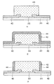
参考例1:図4のAとBとを参照しつつ説明する。図3Aは、複数の絶縁層付角柱状バンプ42を備えたICチップ20の平面図である。ここで、非導電性基板30にはガラス基板を用いた。そして、図4Bは、非導電性基板30とICチップ20を実装した状態で、図4Aに示した絶縁層付角柱状バンプ42の3−3線に沿った断面図である。本発明の第1の好ましい具体例では、絶縁層付角柱状バンプ42は、非導電性基板30の第1ボンディングパッド18とICチップ20の第2ボンディングパッド22とを接合するよう配置している。
【0022】
このときの絶縁層付角柱状バンプ42はICチップ20の第2ボンディングパッド22の上に製造したものであり、絶縁層付角柱状バンプ42の側壁面は、並立して隣接する絶縁層付角柱状バンプ42との電気的絶縁を確保するため、絶縁層付角柱状バンプ42の側壁面の全体が絶縁層44で被覆された状態のものを用いている。
【0023】
そして、非導電性基板30とICチップ20とを重ねて接合すると、ICチップ20の第2ボンディングパッド22の上に設けた絶縁層付角柱状バンプ42が、第1ボンディングパッド18に導電粒子25を介して接合するようにした。ICチップ20と非導電性基板30との張り合わせは、非導電性基板30の表面に設けたACF38の粘着力により行った。このようにして、図4Bに示した構造のチップオングラス製品とすることで、絶縁層付角柱状バンプ42の絶縁層44が、各絶縁層付角柱状バンプ42の側壁に位置することで、相隣接した絶縁層付角柱状バンプ42間に横方向に導通状態を作り出した導電粒子25が存在していても、相隣接した絶縁層付角柱状バンプ42間の電気的ショートを防ぎ、TFTの誤動作を有効に防止することが可能となり、LCDモジュールの機能性と信頼性を大幅に向上させることができる。
【0024】
ここで用いた絶縁層付角柱状バンプ42は、次に述べる方法で、ICチップ20の第2ボンディングパッド22の上に製造した。図5A〜図6Fを参照して説明する。図面上、絶縁層付角柱状バンプ42を形成する第2ボンディングパッド22の一つを拡大断面として模式的に示すものとした。図4で示した絶縁層付角柱状バンプ42の製造フローを断面図として示しているのである。まず、図5Aで示したように、ICチップ20は、その表面に第2ボンディングパッド22と保護層40とを備えている。本実施形態では、第2ボンディングパッド22の材質はアルミニウムであり、ICチップ20上に形成した集積回路を保護する保護層40は窒化物で形成されている。
【0025】
そして、絶縁層付角柱状バンプ42を形成するため、図4Aで示したように、ICチップ20の表面にフォトレジスト層45を形成した。その後、露光工程、現像工程、エッチング工程が順次施されて、フォトレジスト層45の所定領域を除去して、絶縁層付角柱状バンプ42の形状に応じたホール部43を形成し、第2ボンディングパッド22の表面を露出させた。
【0026】
次に、図5Cで示したように、蒸着法を用いて、ホール部43を、絶縁層付角柱状バンプ42の内部を構成する金属材で金属層46を、ホール部43の形状通りに製造した。
【0027】
以上の作業が終了すると、ICチップ20上の表面に硬化して残留しているフォトレジスト層45を除去して、図4Dに示すような状態とした。その後、酸化ケイ素又は窒化ケイ素を蒸着して絶縁層44を、図6Eとして示したように形成することで、絶縁層付角柱状バンプ42の突出面と側壁面とを絶縁被覆した。
【0028】
最後に図6Fで示したように、反応性イオンエッチング(RIE)法を用いて、異方性ドライエッチングを行うことで、絶縁層付角柱状バンプ42の突出面とICチップ20の保護層40との表面に位置する絶縁層44を除去した。このようにすることで、絶縁層付角柱状バンプ42の側壁面の全体にのみ絶縁層44が残るようにした。
【0029】
参考例2:基本的には参考例1と同様であって、本参考例は、ICチップ20上に絶縁層付角柱状バンプ42の製造方法のみが異なるのみである。従って、以下、異なる部分として、絶縁層付角柱状バンプ42の形成方法のみを説明する。
【0030】
また、図7A〜図8Fは、図4で示した絶縁層付角柱状バンプ42のもう一つの製造方法を示す断面図である。本発明の金属突起42の製造方法によると、図7Aで示したように、先ず、フォトレジスト層45を、ICチップ20上に形成した。その後、図7Bで示したように、露光工程、現像工程、レジストエッチング工程を経て、フォトレジスト層45の所定領域を除去して、絶縁層付角柱状バンプ42の形状パターンを形成し、第1ホール部48を形成する。この第1ホール部48は、その底部に第2ボンディングパッド22が露出した形で位置し、第2ボンディングパッド22を取り囲む保護層40の壁部が形成されることになる。
【0031】
次に、図7Cで示したように、絶縁層付角柱状バンプ42の絶縁層44を構成する素材を、ICチップ20に蒸着し、前記第1ホール部48を充填埋設する。そして、図8Dで示したように、絶縁層エッチングを行い、フォトレジスト層45、第2ボンディングパッド22及び保護層40の表面上に位置する絶縁層44を除去し、第1ホール部48の側壁に接する絶縁層44のみを残して、第2ホール部50を形成する。
【0032】
続いて、図8Eで示したように、金属層46を構成する素材をICチップ20に蒸着し、前記第2ホール部50を充填埋設し、その後フォトレジスト層45上に残留する金属層46を除去し、第2ホール部50内に位置する金属層46の表面を平坦に均一化する。
【0033】
最後に図8Fで示したように、硬化したフォトレジスト層45を除去すると、側壁に絶縁層44を備える絶縁層付角柱状バンプ42がICチップ20の第2ボンディングパッド22上に完成したのである。
【0034】
第1実施形態:本実施形態では、絶縁層44を、当該絶縁層付角柱状バンプの4面の側壁面の内、相隣接する2つの側壁面にのみ絶縁層44を形成した絶縁層付角柱状バンプを用いて、チップオングラス製品のICチップ20と非導電性基板30とを電気的に接続した絶縁層付角柱状バンプ同士の絶縁方法について説明する。
【0035】
ここでは図9Aと図9Bを参照するものとする。図9Aは、絶縁層付角柱状バンプ421,422を形成したICチップ20を示した平面図である。そして、図9Bは、非導電性基板30にICチップ20を実装して、絶縁層付角柱状バンプ421,422の部分を6−6線に沿って切断した場合の断面図である。
【0036】
本実施形態においては、説明の都合上、ICチップ20の、第2ボンディングパッド22の上に形成した絶縁層付角柱状バンプは、複数が並立した状態で存在している。そして、この絶縁層付角柱状バンプの内、説明の都合上、図9に示したように、第1絶縁層付角柱状バンプ421と、第2絶縁層付角柱状バンプ422と称し、相隣接し並立した状態にある特定位置の絶縁層付角柱状バンプを示すものとする。このとき、第1絶縁層付角柱状バンプ421と第2絶縁層付角柱状バンプ422とを、図9Aに示すように配置する。
【0037】
その結果、第1絶縁層付角柱状バンプ421の絶縁層44を備えた面521は、第2絶縁層付角柱状バンプ422の絶縁層44を備えていない面522と相対峙することになる。このように配置すれば、第1絶縁層付角柱状バンプ421と第2絶縁層付角柱状バンプ422との側壁面における電気的ショートは防止できるものとなる。即ち、絶縁層付角柱状バンプの4面の側壁面の全てに絶縁層44を形成することなく、バンプ相互間の電気的ショートを有効に防止することが可能となるのである。これによりLCDモジュールの機能性と信頼性を向上させることができるのである。
【0038】
【発明の効果】
本件発明に係る絶縁層付角柱状バンプを用いることで、チップオングラス製品のバンプ相互間のショート不良を解消し、信号伝達時の誤動作を解消することが出来、LCDモジュールを用いる電気、電子製品の品質安定性を高水準化することが可能となる。また、本件発明に係る製造方法を用いることで、効率よく絶縁層付角柱状バンプの製造を行うことが可能であり、大量の製品の市場供給を可能とするものである。
【図面の簡単な説明】
【図1】 従来のチップオングラスの平面図。
【図2】 図1にて示した断面線における断面観察模式図。
【図3】 従来のチップオングラスの断面図。
【図4】 本件発明に係る絶縁層付角柱状バンプを形成したICチップの平面図及びチップオングラスの断面図。
【図5】 本件発明に係る絶縁層付角柱状バンプをICチップ表面に形成するフローを表した断面概念図。
【図6】 本件発明に係る絶縁層付角柱状バンプをICチップ表面に形成するフローを表した断面概念図。
【図7】 本件発明に係る絶縁層付角柱状バンプをICチップ表面に形成するフローを表した断面概念図。
【図8】 本件発明に係る絶縁層付角柱状バンプをICチップ表面に形成するフローを表した断面概念図。
【図9】 本件発明に係る絶縁層付角柱状バンプを形成したICチップの平面図及びチップオングラスの断面図。
【符号の説明】
10 ガラス基板
12 第1領域
14 第2領域
15 データIC搭載部
16 スキャンIC搭載部
17 第3領域
18 第1ボンディングパッド
20 ICチップ
22 第2ボンディングパッド
24 ACF
25 導電粒子
26 バンプ
30 非導電性基板
40 保護層
42 絶縁層付角柱状バンプ
44 絶縁層
46 金属層
48 第1ホール部
50 第2ホール部
421 第1絶縁層付角柱状バンプ
422 第2絶縁層付角柱状バンプ[0001]
BACKGROUND OF THE INVENTION
The present invention relates to a prismatic bump with an insulating layer and a method for manufacturing the same.
[0002]
[Prior art]
Mounting a bare die on a glass panel (chip on glass, referred to as “COG”) electrically connects an integrated circuit (referred to as integrated circuit, “ICs”), and is lightweight. It is an advanced technology that achieves small size, low cost, low power consumption, etc., and is used in various display products. For example, COG is a medium-sized product such as a small display panel of 4 inches or less such as a telephone or a copier having 1 to 2 IC chips, a video camera or a navigation system that requires 3 to 12 IC chips ( 4-11 inch) display panels and large product display panels (11 inches or more) such as notebook personal computers.
[0003]
The quality and reliability of a liquid crystal display (referred to as “LCD”) module is determined by the accuracy with which the driving IC chip is mounted on the glass panel. An anisotropic conductive film (referred to as “ACF”) is the most widely used material for mounting a driving IC chip on a glass panel. ACF is an adhesive film comprising finely dispersed electrically conductive particles having a diameter of 3 to 15 μm and an insulating adhesive film having a thickness of 15 to 35 μm. Until now, the uniformity of the distribution of the conductive particles is thought to affect the electrical properties and reliability of the ACF, and there are a variety of such as carbon fiber, metal (nickel, solder) and plated (nickel / gold) plastic balls. Types of conductive particles have been proposed.
[0004]
Various types of adhesives have also been proposed, such as thermoplastic materials, thermosetting materials, and mixed materials of thermoplastic materials and thermosetting materials. Generally, ACF is divided into two types. One of them contains conductive particles with a diameter of about 5 μm covered with a very thin insulating layer. The conductive particles are sandwiched between bumps on the IC chip and bonding pads on the glass panel, and are bonded. The conductive particles are deformed by pressing, and the thin insulating layer of the conductive particles is torn and the exposed conductive particles are sandwiched between the bumps on the IC chip and the bonding pads on the glass panel. Thus, the bridge functions to ensure electrical continuity between the two.
[0005]
However, as described above, the conductive particles are sandwiched between the bumps on the IC chip and the bonding pads on the glass panel, the conductive particles are deformed by the pressure at the time of bonding, and the thin insulating layer is torn well, Since it is not certain whether or not the conductive particles are exposed as intended, there is a drawback that the electrical continuity between the bumps and the bonding pads is not reliable enough to ensure the design reason.
[0006]
Another type of ACF is a two-layer type, and mainly consists of a resin layer containing conductive particles having a diameter of about 3 μm and a resin layer not containing conductive particles, thereby ensuring mainly conductivity. It is a thing which provided the layer used in order to isolate | separate and the layer mainly used in order to ensure adhesiveness separately. The bumps and the bonding pads are efficiently bonded by separately exerting the intended functions of the respective layers. However, the disadvantage of the ACF having this two-layer structure is that the amount of conductive particles located between the IC chip and the glass panel when the IC chip is bonded to the glass panel via bumps is too large. This makes it easier for current to flow between a plurality of bumps arranged side by side between the IC chip and the glass panel, causing an electrical short between the bumps and causing a malfunction.
[0007]
Here, the prior art will be described with reference to FIGS. FIG. 1A is a plan view of a
[0008]
The data IC
[0009]
2A to 3D are cross-sectional views illustrating a method for mounting the
[0010]
[Problems to be solved by the invention]
However, as shown in FIG. 2D, since it is difficult to control the distribution of the
[0011]
In particular, when the
[0012]
[Means for Solving the Problems]
Therefore, the inventors of the present invention have made the following invention as a solution to the problem by using a bump provided with an insulating layer and to provide a method suitable for manufacturing the bump. .
[0013]
The present invention is a metal prismatic bump used to connect a bonding pad on the non-conductive substrate side and a bonding pad on the IC chip side at a plurality of locations when mounting the IC chip on the non-conductive substrate. The prismatic bump is provided with an insulating layer only on two adjacent side wall surfaces among the four side wall surfaces, and the insulating layer provided on one prismatic bump; A metal in which a prismatic bump and a side surface not provided with an insulating layer of another bump adjacent to each other face each other, and a side wall surface provided with an insulating layer of a prismatic bump is directed in the same direction This is a prismatic bump with an insulating layer made of insulating material.
[0014]
This insulating layer is preferably made of silicon oxide or silicon nitride. The prismatic bumps are preferably made of gold.
[0015]
Moreover, this invention is a chip-on-glass product formed by connecting a non-conductive substrate or an IC chip having the above-described prismatic bumps with an insulating layer. At this time, the non-conductive substrate is preferably a glass substrate. And what filled the space where the prismatic bump with an insulating layer between a nonelectroconductive board | substrate and the said IC chip was inserted with the anisotropic conductive material is preferable.
[0016]
The present invention is a method for integrally manufacturing a prismatic bump with an insulating layer on the surface of the IC chip, which comprises the following steps, and manufacturing an IC chip provided with a prismatic bump with an insulating layer Is the method.
[0017]
(A) A step of forming a photoresist layer on the surface of an IC chip having a plurality of second bonding pads (b) An etching process of the photoresist layer on the second bonding pads by exposing and developing the photoresist layer And (c) covering the entire surface of the IC chip with the constituent material of the insulating layer, and simultaneously filling the constituent material of the insulating layer into the first hole portion. Step (d) A part of the constituent material of the insulating layer on the second bonding pad and the constituent material of the insulating layer located on the surface of the IC chip are removed by anisotropic dry etching, and the first The central portion of the prismatic bump with insulating layer is formed by leaving only the portion for forming the insulating layer that forms the side wall of the prismatic bump with insulating layer on the outer peripheral wall portion of the hole portion. Step [0018] removing the photoresist layer remaining on the step (f) IC chip filling the second hole in the step (e) the metal material forming the second hole fit
This anisotropic dry etching process preferably uses a reactive ion etching (RIE) method.
[0019]
The bump with an insulating layer described above can surely prevent a short circuit between the bumps when using the ACF, thereby greatly improving the functionality and reliability of the LCD module. it can.
[0020]
DETAILED DESCRIPTION OF THE INVENTION
In order to further clarify the above-described objects, features, and advantages of the present invention, preferred embodiments of the present invention will be given below and described in more detail with reference to the drawings.
[0021]
Reference Example 1 : Explanation will be made with reference to FIGS. 4A and 4B. FIG. 3A is a plan view of the
[0022]
The
[0023]
Then, when the
[0024]
The insulating layer-equipped
[0025]
Then, in order to form the
[0026]
Next, as shown in FIG. 5C, the
[0027]
When the above operation is completed, the
[0028]
Finally, as shown in FIG. 6F, anisotropic dry etching is performed using a reactive ion etching (RIE) method, so that the protruding surfaces of the
[0029]
Reference Example 2 : Basically, it is the same as Reference Example 1, and this Reference Example is different only in the manufacturing method of the
[0030]
7A to 8F are cross-sectional views showing another method for manufacturing the
[0031]
Next, as shown in FIG. 7C, a material constituting the insulating
[0032]
Subsequently, as shown in FIG. 8E, the material constituting the
[0033]
Finally, as shown in FIG. 8F, when the
[0034]
First Embodiment : In this embodiment, an insulating
[0035]
Here, FIG. 9A and FIG. 9B shall be referred to. FIG. 9A is a plan view showing the
[0036]
In the present embodiment, for convenience of explanation, a plurality of prismatic bumps with an insulating layer formed on the
[0037]
As a result, the
[0038]
【The invention's effect】
By using the prismatic bumps with an insulating layer according to the present invention, it is possible to eliminate short-circuit defects between bumps of chip-on-glass products, and to eliminate malfunctions during signal transmission. Electric and electronic products using LCD modules It is possible to improve the quality stability of the product. In addition, by using the manufacturing method according to the present invention, it is possible to efficiently manufacture a prismatic bump with an insulating layer, and to supply a large amount of products to the market.
[Brief description of the drawings]
FIG. 1 is a plan view of a conventional chip-on-glass.
2 is a cross-sectional observation schematic diagram taken along a cross-sectional line shown in FIG.
FIG. 3 is a cross-sectional view of a conventional chip-on-glass.
FIG. 4 is a plan view of an IC chip on which a prismatic bump with an insulating layer according to the present invention is formed and a cross-sectional view of chip-on-glass.
FIG. 5 is a conceptual cross-sectional view showing a flow of forming a prismatic bump with an insulating layer according to the present invention on the surface of an IC chip.
FIG. 6 is a conceptual cross-sectional view showing a flow of forming a prismatic bump with an insulating layer according to the present invention on the surface of an IC chip.
FIG. 7 is a conceptual cross-sectional view showing a flow of forming a prismatic bump with an insulating layer according to the present invention on the surface of an IC chip.
FIG. 8 is a conceptual cross-sectional view showing a flow of forming a prismatic bump with an insulating layer according to the present invention on the surface of an IC chip.
FIG. 9 is a plan view of an IC chip on which a prismatic bump with an insulating layer according to the present invention is formed, and a cross-sectional view of chip-on-glass.
[Explanation of symbols]
DESCRIPTION OF
25
Claims (8)
前記角柱状バンプは、その4つの側壁面の内、相隣接する2つの側壁面にのみ絶縁層が設けられており、
一の角柱状バンプに設けられた絶縁層と、前記一の角柱状バンプと隣接する他の角柱状バンプの絶縁層が設けられていない側面とが相対峙するようになっている金属製の絶縁層付角柱状バンプ。When mounting an IC chip on a non-conductive substrate, it is a metal prismatic bump used to connect a bonding pad on the non-conductive substrate side and a bonding pad on the IC chip side at a plurality of locations,
The prismatic bump is provided with an insulating layer only on two adjacent side wall surfaces among the four side wall surfaces,
An insulating layer provided on one prismatic bump and a metal insulation in which the one prismatic bump and the side surface on which the insulating layer of the other prismatic bump adjacent thereto is not provided are opposed to each other. Layered prismatic bump.
(a)複数の第2ボンディングパッドを備えるICチップの表面にフォトレジスト層を形成する工程
(b)当該フォトレジスト層を露光し現像することで、第2ボンディングパット上のフォトレジスト層をエッジング処理し、第2ボンディングパッドを露出させる第1ホール部を形成する工程
(c)ICチップ表面の全体を絶縁層の構成材で被覆し、同時に当該第1ホール部に絶縁層の構成材を充填する工程
(d)異方性ドライエッチング法により、前記第2ボンディングパット上の絶縁層の構成材の一部と前記ICチップの表面に位置する絶縁層の構成材とを除去して、当該第1ホール部の外周壁部に前記絶縁層付角柱状バンプの側壁を構成することとなる絶縁層を形成する部位のみを残し、前記絶縁層付角柱状バンプの中心部を形成するための第2ホールを形成する工程
(e)金属材で前記第2ホールを充填する工程
(f)ICチップ上に残留しているフォトレジスト層を除去する工程A method for manufacturing a prismatic bump with an insulating layer integrally on the surface of the IC chip, the manufacturing method of the IC chip comprising the prismatic bump with an insulating layer comprising the following steps.
(A) A step of forming a photoresist layer on the surface of an IC chip having a plurality of second bonding pads (b) An edging process for the photoresist layer on the second bonding pad by exposing and developing the photoresist layer And (c) covering the entire surface of the IC chip with the constituent material of the insulating layer, and simultaneously filling the constituent material of the insulating layer into the first hole portion. Step (d) A part of the constituent material of the insulating layer on the second bonding pad and the constituent material of the insulating layer located on the surface of the IC chip are removed by anisotropic dry etching, and the first The central portion of the prismatic bump with insulating layer is formed by leaving only the portion for forming the insulating layer that forms the side wall of the prismatic bump with insulating layer on the outer peripheral wall portion of the hole portion. Removing the photoresist layer remaining on the step (f) IC chip filling the second hole in the step (e) the metal material forming the second hole fit
Applications Claiming Priority (2)
| Application Number | Priority Date | Filing Date | Title |
|---|---|---|---|
| TW089117464A TW464927B (en) | 2000-08-29 | 2000-08-29 | Metal bump with an insulating sidewall and method of fabricating thereof |
| TW089117464 | 2000-08-29 |
Publications (2)
| Publication Number | Publication Date |
|---|---|
| JP2002118138A JP2002118138A (en) | 2002-04-19 |
| JP3671192B2 true JP3671192B2 (en) | 2005-07-13 |
Family
ID=21660945
Family Applications (1)
| Application Number | Title | Priority Date | Filing Date |
|---|---|---|---|
| JP2001246861A Expired - Fee Related JP3671192B2 (en) | 2000-08-29 | 2001-08-16 | Insulating layered prismatic bump, chip-on-glass product using the bump, and method of manufacturing prismatic bump with insulating layer on the IC chip surface |
Country Status (3)
| Country | Link |
|---|---|
| US (2) | US6958539B2 (en) |
| JP (1) | JP3671192B2 (en) |
| TW (1) | TW464927B (en) |
Families Citing this family (47)
| Publication number | Priority date | Publication date | Assignee | Title |
|---|---|---|---|---|
| US6642136B1 (en) | 2001-09-17 | 2003-11-04 | Megic Corporation | Method of making a low fabrication cost, high performance, high reliability chip scale package |
| US7099293B2 (en) | 2002-05-01 | 2006-08-29 | Stmicroelectronics, Inc. | Buffer-less de-skewing for symbol combination in a CDMA demodulator |
| KR100455387B1 (en) * | 2002-05-17 | 2004-11-06 | 삼성전자주식회사 | Method for forming a bump on semiconductor chip and COG package including the bump |
| WO2004051732A1 (en) * | 2002-11-29 | 2004-06-17 | Infineon Technologies Ag | Attachment of flip-chips to substrates |
| CN1823410A (en) * | 2003-07-16 | 2006-08-23 | 皇家飞利浦电子股份有限公司 | Metal bump with an insulation for the side walls and method of fabricating a chip with such a metal bump |
| US7960830B2 (en) * | 2003-11-14 | 2011-06-14 | Industrial Technology Research Institute | Electronic assembly having a multilayer adhesive structure |
| US8604613B2 (en) * | 2003-11-14 | 2013-12-10 | Industrial Technology Research Institute | Electronic assembly having a multilayer adhesive structure |
| US20050104225A1 (en) * | 2003-11-19 | 2005-05-19 | Yuan-Chang Huang | Conductive bumps with insulating sidewalls and method for fabricating |
| US20060157869A1 (en) * | 2003-11-19 | 2006-07-20 | Industrial Technology Research Institute | Semiconductor substrate with conductive bumps having a stress relief buffer layer formed of an electrically insulating organic material |
| KR100632472B1 (en) * | 2004-04-14 | 2006-10-09 | 삼성전자주식회사 | Microelectronic device chip having a fine pitch bump structure having non-conductive sidewalls, a package thereof, a liquid crystal display device comprising the same, and a manufacturing method thereof |
| CN100527398C (en) * | 2004-04-14 | 2009-08-12 | 三星电子株式会社 | Bump structure for a semiconductor device and method of manufacture |
| US7253089B2 (en) * | 2004-06-14 | 2007-08-07 | Micron Technology, Inc. | Microfeature devices and methods for manufacturing microfeature devices |
| US7465654B2 (en) | 2004-07-09 | 2008-12-16 | Megica Corporation | Structure of gold bumps and gold conductors on one IC die and methods of manufacturing the structures |
| US8022544B2 (en) * | 2004-07-09 | 2011-09-20 | Megica Corporation | Chip structure |
| TWI262347B (en) * | 2004-08-02 | 2006-09-21 | Hannstar Display Corp | Electrical conducting structure and liquid crystal display device comprising the same |
| US7452803B2 (en) * | 2004-08-12 | 2008-11-18 | Megica Corporation | Method for fabricating chip structure |
| US7547969B2 (en) | 2004-10-29 | 2009-06-16 | Megica Corporation | Semiconductor chip with passivation layer comprising metal interconnect and contact pads |
| TWI393226B (en) * | 2004-11-04 | 2013-04-11 | Taiwan Semiconductor Mfg | Nanotube-based filler |
| CN1901163B (en) * | 2005-07-22 | 2011-04-13 | 米辑电子股份有限公司 | Method for fabricating a circuitry component by continuous electroplating and circuitry component structure |
| US7397121B2 (en) | 2005-10-28 | 2008-07-08 | Megica Corporation | Semiconductor chip with post-passivation scheme formed over passivation layer |
| US20070238222A1 (en) | 2006-03-28 | 2007-10-11 | Harries Richard J | Apparatuses and methods to enhance passivation and ILD reliability |
| JP4768491B2 (en) * | 2006-03-30 | 2011-09-07 | Okiセミコンダクタ株式会社 | Manufacturing method of semiconductor device |
| TWI346826B (en) * | 2006-10-26 | 2011-08-11 | Taiwan Tft Lcd Ass | Bonding structure and method of fabricating the same |
| TWI334183B (en) * | 2007-02-15 | 2010-12-01 | Chipmos Technologies Inc | Conductive structure for a semiconductor integrated circuit and method for forming the same |
| US9093322B2 (en) * | 2007-07-13 | 2015-07-28 | Intel Mobile Communications GmbH | Semiconductor device |
| US9524945B2 (en) | 2010-05-18 | 2016-12-20 | Taiwan Semiconductor Manufacturing Company, Ltd. | Cu pillar bump with L-shaped non-metal sidewall protection structure |
| US8377816B2 (en) * | 2009-07-30 | 2013-02-19 | Taiwan Semiconductor Manufacturing Company, Ltd. | Method of forming electrical connections |
| US8841766B2 (en) * | 2009-07-30 | 2014-09-23 | Taiwan Semiconductor Manufacturing Company, Ltd. | Cu pillar bump with non-metal sidewall protection structure |
| US8324738B2 (en) | 2009-09-01 | 2012-12-04 | Taiwan Semiconductor Manufacturing Company, Ltd. | Self-aligned protection layer for copper post structure |
| US8659155B2 (en) | 2009-11-05 | 2014-02-25 | Taiwan Semiconductor Manufacturing Company, Ltd. | Mechanisms for forming copper pillar bumps |
| TW201121006A (en) * | 2009-12-03 | 2011-06-16 | Hannstar Display Corp | Connection structure for chip-on-glass driver IC and connection method therefor |
| US8610270B2 (en) | 2010-02-09 | 2013-12-17 | Taiwan Semiconductor Manufacturing Company, Ltd. | Semiconductor device and semiconductor assembly with lead-free solder |
| US8441124B2 (en) | 2010-04-29 | 2013-05-14 | Taiwan Semiconductor Manufacturing Company, Ltd. | Cu pillar bump with non-metal sidewall protection structure |
| TWI419284B (en) * | 2010-05-26 | 2013-12-11 | Chipmos Technologies Inc | Chip bump structure and method for forming chip bump structure |
| US9018758B2 (en) | 2010-06-02 | 2015-04-28 | Taiwan Semiconductor Manufacturing Company, Ltd. | Cu pillar bump with non-metal sidewall spacer and metal top cap |
| US8546254B2 (en) | 2010-08-19 | 2013-10-01 | Taiwan Semiconductor Manufacturing Company, Ltd. | Mechanisms for forming copper pillar bumps using patterned anodes |
| WO2012107971A1 (en) * | 2011-02-10 | 2012-08-16 | パナソニック株式会社 | Semiconductor device and method for manufacturing same |
| US8692390B2 (en) | 2011-02-18 | 2014-04-08 | Chipbond Technology Corporation | Pyramid bump structure |
| JP5664392B2 (en) * | 2011-03-23 | 2015-02-04 | ソニー株式会社 | Semiconductor device, method for manufacturing semiconductor device, and method for manufacturing wiring board |
| US10276402B2 (en) * | 2016-03-21 | 2019-04-30 | Taiwan Semiconductor Manufacturing Co., Ltd. | Semiconductor package and manufacturing process thereof |
| US10049893B2 (en) * | 2016-05-11 | 2018-08-14 | Advanced Semiconductor Engineering, Inc. | Semiconductor device with a conductive post |
| JP7046351B2 (en) | 2018-01-31 | 2022-04-04 | 三国電子有限会社 | How to make a connection structure |
| JP7160302B2 (en) * | 2018-01-31 | 2022-10-25 | 三国電子有限会社 | CONNECTED STRUCTURE AND METHOD OF MAKING CONNECTED STRUCTURE |
| JP7185252B2 (en) | 2018-01-31 | 2022-12-07 | 三国電子有限会社 | Method for producing connection structure |
| US20210159198A1 (en) * | 2019-11-24 | 2021-05-27 | Nanya Technology Corporation | Semiconductor structure and manufacturing method thereof |
| CN110930879B (en) * | 2019-11-25 | 2020-11-10 | 武汉华星光电半导体显示技术有限公司 | Display device |
| US20230014450A1 (en) * | 2021-07-16 | 2023-01-19 | Taiwan Semiconductor Manufacturing Company, Ltd. | Package structure and method of forming the same |
Family Cites Families (27)
| Publication number | Priority date | Publication date | Assignee | Title |
|---|---|---|---|---|
| JPS6444049A (en) * | 1987-08-12 | 1989-02-16 | Fujitsu Ltd | Electrode for flip chip bonding |
| JPH02220863A (en) | 1989-02-23 | 1990-09-04 | Minolta Camera Co Ltd | Printer |
| JP2928822B2 (en) * | 1990-02-02 | 1999-08-03 | カシオ計算機株式会社 | Semiconductor device and connection method thereof |
| JPH04196434A (en) * | 1990-11-28 | 1992-07-16 | Seiko Epson Corp | Manufacture of semiconductor device |
| JPH068599A (en) | 1992-06-29 | 1994-01-18 | Brother Ind Ltd | Printer |
| JPH06232211A (en) * | 1993-02-03 | 1994-08-19 | Casio Comput Co Ltd | Connecting structure of ic chip, and connecting method thereof |
| JPH0872486A (en) | 1994-08-31 | 1996-03-19 | Akihiro Aoki | Measure having reduction scale |
| US5578527A (en) * | 1995-06-23 | 1996-11-26 | Industrial Technology Research Institute | Connection construction and method of manufacturing the same |
| KR0157905B1 (en) * | 1995-10-19 | 1998-12-01 | 문정환 | Semiconductor device |
| KR100225398B1 (en) | 1995-12-01 | 1999-10-15 | 구자홍 | Bonding structure of semiconductor bump and its method |
| US6232563B1 (en) * | 1995-11-25 | 2001-05-15 | Lg Electronics Inc. | Bump electrode and method for fabricating the same |
| KR0171099B1 (en) | 1995-11-25 | 1999-02-01 | 구자홍 | Substrate bumb and the same manufacture method |
| KR100232678B1 (en) * | 1996-12-18 | 1999-12-01 | 구본준 | A structure and a method of ridged bump |
| JP3328157B2 (en) * | 1997-03-06 | 2002-09-24 | シャープ株式会社 | Liquid crystal display |
| US5783465A (en) * | 1997-04-03 | 1998-07-21 | Lucent Technologies Inc. | Compliant bump technology |
| US6683384B1 (en) * | 1997-10-08 | 2004-01-27 | Agere Systems Inc | Air isolated crossovers |
| US6157079A (en) * | 1997-11-10 | 2000-12-05 | Citizen Watch Co., Ltd | Semiconductor device with a bump including a bump electrode film covering a projecting photoresist |
| TW366548B (en) * | 1998-04-18 | 1999-08-11 | United Microelectronics Corp | Trench bump block and the application of the same |
| KR100347762B1 (en) * | 1999-12-15 | 2002-08-09 | 엘지전자주식회사 | Direct attatch bonding process of bare chip and pwb |
| JP2001244289A (en) * | 1999-12-24 | 2001-09-07 | Seiko Epson Corp | Semiconductor device and method of manufacturing the same |
| JP4663165B2 (en) * | 2001-06-27 | 2011-03-30 | ルネサスエレクトロニクス株式会社 | Semiconductor device and manufacturing method thereof |
| JP2004134653A (en) * | 2002-10-11 | 2004-04-30 | Sharp Corp | Substrate connecting structure and fabricating process of electronic parts therewith |
| US7088004B2 (en) * | 2002-11-27 | 2006-08-08 | International Rectifier Corporation | Flip-chip device having conductive connectors |
| JP3964319B2 (en) * | 2002-12-20 | 2007-08-22 | セイコーインスツル株式会社 | Semiconductor device |
| JP4115832B2 (en) * | 2002-12-27 | 2008-07-09 | 東芝松下ディスプレイテクノロジー株式会社 | Semiconductor device and liquid crystal display panel |
| US7242097B2 (en) * | 2003-06-30 | 2007-07-10 | Intel Corporation | Electromigration barrier layers for solder joints |
| US20050082670A1 (en) * | 2003-09-11 | 2005-04-21 | Nordson Corporation | Method for preapplying a viscous material to strengthen solder connections in microelectronic packaging and microelectronic packages formed thereby |
-
2000
- 2000-08-29 TW TW089117464A patent/TW464927B/en not_active IP Right Cessation
-
2001
- 2001-01-19 US US09/764,207 patent/US6958539B2/en not_active Expired - Lifetime
- 2001-08-16 JP JP2001246861A patent/JP3671192B2/en not_active Expired - Fee Related
-
2003
- 2003-09-08 US US10/656,248 patent/US7041589B2/en not_active Expired - Lifetime
Also Published As
| Publication number | Publication date |
|---|---|
| US20020048924A1 (en) | 2002-04-25 |
| US7041589B2 (en) | 2006-05-09 |
| TW464927B (en) | 2001-11-21 |
| US6958539B2 (en) | 2005-10-25 |
| JP2002118138A (en) | 2002-04-19 |
| US20040048202A1 (en) | 2004-03-11 |
Similar Documents
| Publication | Publication Date | Title |
|---|---|---|
| JP3671192B2 (en) | Insulating layered prismatic bump, chip-on-glass product using the bump, and method of manufacturing prismatic bump with insulating layer on the IC chip surface | |
| US7492434B2 (en) | Display device having an anisotropic-conductive adhesive film | |
| CN110544434B (en) | Display panel, manufacturing method thereof and display device | |
| US7763986B2 (en) | Semiconductor chip, film substrate, and related semiconductor chip package | |
| US7916262B2 (en) | Signal transmission assembly and display device applied with the same | |
| JP2000221540A (en) | Active matrix type liquid crystal display device | |
| US20070242207A1 (en) | Flat display panel and connection structure | |
| JP2004214374A (en) | Semiconductor device and liquid-crystal display panel | |
| US20040099959A1 (en) | Conductive bump structure | |
| JP2002252249A (en) | Metal bump | |
| KR100531590B1 (en) | Liquid crystal display and method for manufacturing the same | |
| JP2009054833A (en) | Ectronic device and its manufacturing emthod, electrooptical device, and electronic device | |
| US8174110B2 (en) | Semiconductor device having at least two terminals among the plurality of terminals electrically connected to each other while not being adjacent to one other and not being connected to internal circuit | |
| JP2009081416A (en) | Semiconductor device, semiconductor mounting structure, and electro-optical device | |
| JP3810064B2 (en) | Liquid crystal display | |
| JP2006163012A (en) | Display panel, display apparatus using the same and method for manufacturing display panel | |
| JP2000111939A (en) | Liquid crystal display device | |
| JPH10144727A (en) | Mounting of semiconductor element and electronic device mounted with semiconductor element | |
| JP2000208178A (en) | Semiconductor application device and its production | |
| TWI483402B (en) | A contact circuit | |
| JPH0951018A (en) | Semiconductor device and its manufacturing method | |
| JP2002344097A (en) | Mounting substrate and display device having the same | |
| JP2002196703A (en) | Package structure of semiconductor elements and liquid crystal display device having the structure | |
| TWI390691B (en) | Bonding pad, chip-on-glass package and liquid crystal display panel | |
| KR101100133B1 (en) | Chip On Glass mode LCD device |
Legal Events
| Date | Code | Title | Description |
|---|---|---|---|
| A131 | Notification of reasons for refusal |
Free format text: JAPANESE INTERMEDIATE CODE: A131 Effective date: 20040426 |
|
| A521 | Request for written amendment filed |
Free format text: JAPANESE INTERMEDIATE CODE: A523 Effective date: 20040720 |
|
| A131 | Notification of reasons for refusal |
Free format text: JAPANESE INTERMEDIATE CODE: A131 Effective date: 20040809 |
|
| A521 | Request for written amendment filed |
Free format text: JAPANESE INTERMEDIATE CODE: A523 Effective date: 20041108 |
|
| A521 | Request for written amendment filed |
Free format text: JAPANESE INTERMEDIATE CODE: A523 Effective date: 20041118 |
|
| TRDD | Decision of grant or rejection written | ||
| A01 | Written decision to grant a patent or to grant a registration (utility model) |
Free format text: JAPANESE INTERMEDIATE CODE: A01 Effective date: 20041209 |
|
| A711 | Notification of change in applicant |
Free format text: JAPANESE INTERMEDIATE CODE: A712 Effective date: 20050107 |
|
| A61 | First payment of annual fees (during grant procedure) |
Free format text: JAPANESE INTERMEDIATE CODE: A61 Effective date: 20050107 |
|
| A521 | Request for written amendment filed |
Free format text: JAPANESE INTERMEDIATE CODE: A523 Effective date: 20050124 |
|
| A521 | Request for written amendment filed |
Free format text: JAPANESE INTERMEDIATE CODE: A523 Effective date: 20050322 |
|
| A521 | Request for written amendment filed |
Free format text: JAPANESE INTERMEDIATE CODE: A821 Effective date: 20050323 |
|
| R150 | Certificate of patent or registration of utility model |
Ref document number: 3671192 Country of ref document: JP Free format text: JAPANESE INTERMEDIATE CODE: R150 Free format text: JAPANESE INTERMEDIATE CODE: R150 |
|
| A072 | Dismissal of procedure [no reply to invitation to correct request for examination] |
Free format text: JAPANESE INTERMEDIATE CODE: A072 Effective date: 20050613 |
|
| FPAY | Renewal fee payment (event date is renewal date of database) |
Free format text: PAYMENT UNTIL: 20090428 Year of fee payment: 4 |
|
| R250 | Receipt of annual fees |
Free format text: JAPANESE INTERMEDIATE CODE: R250 |
|
| FPAY | Renewal fee payment (event date is renewal date of database) |
Free format text: PAYMENT UNTIL: 20090428 Year of fee payment: 4 |
|
| FPAY | Renewal fee payment (event date is renewal date of database) |
Free format text: PAYMENT UNTIL: 20100428 Year of fee payment: 5 |
|
| R250 | Receipt of annual fees |
Free format text: JAPANESE INTERMEDIATE CODE: R250 |
|
| FPAY | Renewal fee payment (event date is renewal date of database) |
Free format text: PAYMENT UNTIL: 20100428 Year of fee payment: 5 |
|
| FPAY | Renewal fee payment (event date is renewal date of database) |
Free format text: PAYMENT UNTIL: 20110428 Year of fee payment: 6 |
|
| R250 | Receipt of annual fees |
Free format text: JAPANESE INTERMEDIATE CODE: R250 |
|
| FPAY | Renewal fee payment (event date is renewal date of database) |
Free format text: PAYMENT UNTIL: 20120428 Year of fee payment: 7 |
|
| R250 | Receipt of annual fees |
Free format text: JAPANESE INTERMEDIATE CODE: R250 |
|
| FPAY | Renewal fee payment (event date is renewal date of database) |
Free format text: PAYMENT UNTIL: 20120428 Year of fee payment: 7 |
|
| FPAY | Renewal fee payment (event date is renewal date of database) |
Free format text: PAYMENT UNTIL: 20130428 Year of fee payment: 8 |
|
| R250 | Receipt of annual fees |
Free format text: JAPANESE INTERMEDIATE CODE: R250 |
|
| FPAY | Renewal fee payment (event date is renewal date of database) |
Free format text: PAYMENT UNTIL: 20130428 Year of fee payment: 8 |
|
| FPAY | Renewal fee payment (event date is renewal date of database) |
Free format text: PAYMENT UNTIL: 20140428 Year of fee payment: 9 |
|
| R250 | Receipt of annual fees |
Free format text: JAPANESE INTERMEDIATE CODE: R250 |
|
| R250 | Receipt of annual fees |
Free format text: JAPANESE INTERMEDIATE CODE: R250 |
|
| R250 | Receipt of annual fees |
Free format text: JAPANESE INTERMEDIATE CODE: R250 |
|
| R250 | Receipt of annual fees |
Free format text: JAPANESE INTERMEDIATE CODE: R250 |
|
| R250 | Receipt of annual fees |
Free format text: JAPANESE INTERMEDIATE CODE: R250 |
|
| R250 | Receipt of annual fees |
Free format text: JAPANESE INTERMEDIATE CODE: R250 |
|
| R250 | Receipt of annual fees |
Free format text: JAPANESE INTERMEDIATE CODE: R250 |
|
| R250 | Receipt of annual fees |
Free format text: JAPANESE INTERMEDIATE CODE: R250 |
|
| LAPS | Cancellation because of no payment of annual fees |