JP2021032934A - フレキシブル配線基板、電気光学装置および電子機器 - Google Patents
フレキシブル配線基板、電気光学装置および電子機器 Download PDFInfo
- Publication number
- JP2021032934A JP2021032934A JP2019149680A JP2019149680A JP2021032934A JP 2021032934 A JP2021032934 A JP 2021032934A JP 2019149680 A JP2019149680 A JP 2019149680A JP 2019149680 A JP2019149680 A JP 2019149680A JP 2021032934 A JP2021032934 A JP 2021032934A
- Authority
- JP
- Japan
- Prior art keywords
- wiring board
- flexible wiring
- electro
- insulating member
- substrate
- Prior art date
- Legal status (The legal status is an assumption and is not a legal conclusion. Google has not performed a legal analysis and makes no representation as to the accuracy of the status listed.)
- Granted
Links
- 239000000758 substrate Substances 0.000 claims abstract description 142
- 230000001681 protective effect Effects 0.000 claims abstract description 98
- 239000004065 semiconductor Substances 0.000 claims description 53
- 239000000463 material Substances 0.000 claims description 35
- 239000011347 resin Substances 0.000 claims description 26
- 229920005989 resin Polymers 0.000 claims description 26
- 239000004642 Polyimide Substances 0.000 claims description 16
- 229920001721 polyimide Polymers 0.000 claims description 16
- 229910000679 solder Inorganic materials 0.000 claims description 10
- XUIMIQQOPSSXEZ-UHFFFAOYSA-N Silicon Chemical compound [Si] XUIMIQQOPSSXEZ-UHFFFAOYSA-N 0.000 abstract description 39
- 229910052710 silicon Inorganic materials 0.000 abstract description 39
- 239000010703 silicon Substances 0.000 abstract description 39
- 238000009413 insulation Methods 0.000 abstract description 2
- 239000004973 liquid crystal related substance Substances 0.000 description 35
- 239000000853 adhesive Substances 0.000 description 14
- 230000001070 adhesive effect Effects 0.000 description 14
- 239000011521 glass Substances 0.000 description 14
- 230000003287 optical effect Effects 0.000 description 13
- 238000005070 sampling Methods 0.000 description 8
- 238000000034 method Methods 0.000 description 7
- 230000003014 reinforcing effect Effects 0.000 description 6
- RYGMFSIKBFXOCR-UHFFFAOYSA-N Copper Chemical compound [Cu] RYGMFSIKBFXOCR-UHFFFAOYSA-N 0.000 description 5
- 239000011159 matrix material Substances 0.000 description 5
- 230000004048 modification Effects 0.000 description 5
- 238000012986 modification Methods 0.000 description 5
- 229910052802 copper Inorganic materials 0.000 description 4
- 239000010949 copper Substances 0.000 description 4
- 230000004907 flux Effects 0.000 description 4
- 238000005452 bending Methods 0.000 description 3
- 238000004519 manufacturing process Methods 0.000 description 3
- 210000001525 retina Anatomy 0.000 description 3
- 239000003566 sealing material Substances 0.000 description 3
- 229920001187 thermosetting polymer Polymers 0.000 description 3
- 238000010438 heat treatment Methods 0.000 description 2
- 239000002184 metal Substances 0.000 description 2
- 229910052751 metal Inorganic materials 0.000 description 2
- 238000007639 printing Methods 0.000 description 2
- 238000007650 screen-printing Methods 0.000 description 2
- 230000005540 biological transmission Effects 0.000 description 1
- 239000000919 ceramic Substances 0.000 description 1
- 239000011248 coating agent Substances 0.000 description 1
- 238000000576 coating method Methods 0.000 description 1
- 239000011889 copper foil Substances 0.000 description 1
- 230000007547 defect Effects 0.000 description 1
- 238000005401 electroluminescence Methods 0.000 description 1
- 238000009713 electroplating Methods 0.000 description 1
- 238000005530 etching Methods 0.000 description 1
- 238000000605 extraction Methods 0.000 description 1
- 239000011888 foil Substances 0.000 description 1
- 230000002452 interceptive effect Effects 0.000 description 1
- 229910021421 monocrystalline silicon Inorganic materials 0.000 description 1
- -1 or the like Substances 0.000 description 1
- 230000003647 oxidation Effects 0.000 description 1
- 238000007254 oxidation reaction Methods 0.000 description 1
- 230000000149 penetrating effect Effects 0.000 description 1
- 230000008569 process Effects 0.000 description 1
- 230000004044 response Effects 0.000 description 1
- 239000000126 substance Substances 0.000 description 1
Images


Classifications
-
- G—PHYSICS
- G02—OPTICS
- G02F—OPTICAL DEVICES OR ARRANGEMENTS FOR THE CONTROL OF LIGHT BY MODIFICATION OF THE OPTICAL PROPERTIES OF THE MEDIA OF THE ELEMENTS INVOLVED THEREIN; NON-LINEAR OPTICS; FREQUENCY-CHANGING OF LIGHT; OPTICAL LOGIC ELEMENTS; OPTICAL ANALOGUE/DIGITAL CONVERTERS
- G02F1/00—Devices or arrangements for the control of the intensity, colour, phase, polarisation or direction of light arriving from an independent light source, e.g. switching, gating or modulating; Non-linear optics
- G02F1/01—Devices or arrangements for the control of the intensity, colour, phase, polarisation or direction of light arriving from an independent light source, e.g. switching, gating or modulating; Non-linear optics for the control of the intensity, phase, polarisation or colour
- G02F1/13—Devices or arrangements for the control of the intensity, colour, phase, polarisation or direction of light arriving from an independent light source, e.g. switching, gating or modulating; Non-linear optics for the control of the intensity, phase, polarisation or colour based on liquid crystals, e.g. single liquid crystal display cells
- G02F1/133—Constructional arrangements; Operation of liquid crystal cells; Circuit arrangements
- G02F1/1333—Constructional arrangements; Manufacturing methods
- G02F1/1345—Conductors connecting electrodes to cell terminals
-
- H—ELECTRICITY
- H05—ELECTRIC TECHNIQUES NOT OTHERWISE PROVIDED FOR
- H05K—PRINTED CIRCUITS; CASINGS OR CONSTRUCTIONAL DETAILS OF ELECTRIC APPARATUS; MANUFACTURE OF ASSEMBLAGES OF ELECTRICAL COMPONENTS
- H05K1/00—Printed circuits
- H05K1/02—Details
- H05K1/0277—Bendability or stretchability details
- H05K1/028—Bending or folding regions of flexible printed circuits
-
- G—PHYSICS
- G02—OPTICS
- G02F—OPTICAL DEVICES OR ARRANGEMENTS FOR THE CONTROL OF LIGHT BY MODIFICATION OF THE OPTICAL PROPERTIES OF THE MEDIA OF THE ELEMENTS INVOLVED THEREIN; NON-LINEAR OPTICS; FREQUENCY-CHANGING OF LIGHT; OPTICAL LOGIC ELEMENTS; OPTICAL ANALOGUE/DIGITAL CONVERTERS
- G02F1/00—Devices or arrangements for the control of the intensity, colour, phase, polarisation or direction of light arriving from an independent light source, e.g. switching, gating or modulating; Non-linear optics
- G02F1/01—Devices or arrangements for the control of the intensity, colour, phase, polarisation or direction of light arriving from an independent light source, e.g. switching, gating or modulating; Non-linear optics for the control of the intensity, phase, polarisation or colour
- G02F1/13—Devices or arrangements for the control of the intensity, colour, phase, polarisation or direction of light arriving from an independent light source, e.g. switching, gating or modulating; Non-linear optics for the control of the intensity, phase, polarisation or colour based on liquid crystals, e.g. single liquid crystal display cells
- G02F1/133—Constructional arrangements; Operation of liquid crystal cells; Circuit arrangements
- G02F1/1333—Constructional arrangements; Manufacturing methods
- G02F1/1345—Conductors connecting electrodes to cell terminals
- G02F1/13452—Conductors connecting driver circuitry and terminals of panels
-
- G—PHYSICS
- G02—OPTICS
- G02F—OPTICAL DEVICES OR ARRANGEMENTS FOR THE CONTROL OF LIGHT BY MODIFICATION OF THE OPTICAL PROPERTIES OF THE MEDIA OF THE ELEMENTS INVOLVED THEREIN; NON-LINEAR OPTICS; FREQUENCY-CHANGING OF LIGHT; OPTICAL LOGIC ELEMENTS; OPTICAL ANALOGUE/DIGITAL CONVERTERS
- G02F1/00—Devices or arrangements for the control of the intensity, colour, phase, polarisation or direction of light arriving from an independent light source, e.g. switching, gating or modulating; Non-linear optics
- G02F1/01—Devices or arrangements for the control of the intensity, colour, phase, polarisation or direction of light arriving from an independent light source, e.g. switching, gating or modulating; Non-linear optics for the control of the intensity, phase, polarisation or colour
- G02F1/13—Devices or arrangements for the control of the intensity, colour, phase, polarisation or direction of light arriving from an independent light source, e.g. switching, gating or modulating; Non-linear optics for the control of the intensity, phase, polarisation or colour based on liquid crystals, e.g. single liquid crystal display cells
- G02F1/133—Constructional arrangements; Operation of liquid crystal cells; Circuit arrangements
- G02F1/1333—Constructional arrangements; Manufacturing methods
- G02F1/1345—Conductors connecting electrodes to cell terminals
- G02F1/13456—Cell terminals located on one side of the display only
-
- G—PHYSICS
- G02—OPTICS
- G02F—OPTICAL DEVICES OR ARRANGEMENTS FOR THE CONTROL OF LIGHT BY MODIFICATION OF THE OPTICAL PROPERTIES OF THE MEDIA OF THE ELEMENTS INVOLVED THEREIN; NON-LINEAR OPTICS; FREQUENCY-CHANGING OF LIGHT; OPTICAL LOGIC ELEMENTS; OPTICAL ANALOGUE/DIGITAL CONVERTERS
- G02F1/00—Devices or arrangements for the control of the intensity, colour, phase, polarisation or direction of light arriving from an independent light source, e.g. switching, gating or modulating; Non-linear optics
- G02F1/01—Devices or arrangements for the control of the intensity, colour, phase, polarisation or direction of light arriving from an independent light source, e.g. switching, gating or modulating; Non-linear optics for the control of the intensity, phase, polarisation or colour
- G02F1/13—Devices or arrangements for the control of the intensity, colour, phase, polarisation or direction of light arriving from an independent light source, e.g. switching, gating or modulating; Non-linear optics for the control of the intensity, phase, polarisation or colour based on liquid crystals, e.g. single liquid crystal display cells
- G02F1/133—Constructional arrangements; Operation of liquid crystal cells; Circuit arrangements
- G02F1/1333—Constructional arrangements; Manufacturing methods
- G02F1/1345—Conductors connecting electrodes to cell terminals
- G02F1/13458—Terminal pads
-
- H—ELECTRICITY
- H05—ELECTRIC TECHNIQUES NOT OTHERWISE PROVIDED FOR
- H05K—PRINTED CIRCUITS; CASINGS OR CONSTRUCTIONAL DETAILS OF ELECTRIC APPARATUS; MANUFACTURE OF ASSEMBLAGES OF ELECTRICAL COMPONENTS
- H05K1/00—Printed circuits
- H05K1/02—Details
- H05K1/03—Use of materials for the substrate
- H05K1/0313—Organic insulating material
- H05K1/032—Organic insulating material consisting of one material
- H05K1/0346—Organic insulating material consisting of one material containing N
-
- H—ELECTRICITY
- H05—ELECTRIC TECHNIQUES NOT OTHERWISE PROVIDED FOR
- H05K—PRINTED CIRCUITS; CASINGS OR CONSTRUCTIONAL DETAILS OF ELECTRIC APPARATUS; MANUFACTURE OF ASSEMBLAGES OF ELECTRICAL COMPONENTS
- H05K1/00—Printed circuits
- H05K1/02—Details
- H05K1/11—Printed elements for providing electric connections to or between printed circuits
- H05K1/118—Printed elements for providing electric connections to or between printed circuits specially for flexible printed circuits, e.g. using folded portions
-
- H—ELECTRICITY
- H05—ELECTRIC TECHNIQUES NOT OTHERWISE PROVIDED FOR
- H05K—PRINTED CIRCUITS; CASINGS OR CONSTRUCTIONAL DETAILS OF ELECTRIC APPARATUS; MANUFACTURE OF ASSEMBLAGES OF ELECTRICAL COMPONENTS
- H05K1/00—Printed circuits
- H05K1/18—Printed circuits structurally associated with non-printed electric components
- H05K1/189—Printed circuits structurally associated with non-printed electric components characterised by the use of a flexible or folded printed circuit
-
- G—PHYSICS
- G02—OPTICS
- G02B—OPTICAL ELEMENTS, SYSTEMS OR APPARATUS
- G02B27/00—Optical systems or apparatus not provided for by any of the groups G02B1/00 - G02B26/00, G02B30/00
- G02B27/01—Head-up displays
- G02B27/017—Head mounted
-
- H—ELECTRICITY
- H05—ELECTRIC TECHNIQUES NOT OTHERWISE PROVIDED FOR
- H05K—PRINTED CIRCUITS; CASINGS OR CONSTRUCTIONAL DETAILS OF ELECTRIC APPARATUS; MANUFACTURE OF ASSEMBLAGES OF ELECTRICAL COMPONENTS
- H05K1/00—Printed circuits
- H05K1/02—Details
- H05K1/14—Structural association of two or more printed circuits
- H05K1/147—Structural association of two or more printed circuits at least one of the printed circuits being bent or folded, e.g. by using a flexible printed circuit
-
- H—ELECTRICITY
- H05—ELECTRIC TECHNIQUES NOT OTHERWISE PROVIDED FOR
- H05K—PRINTED CIRCUITS; CASINGS OR CONSTRUCTIONAL DETAILS OF ELECTRIC APPARATUS; MANUFACTURE OF ASSEMBLAGES OF ELECTRICAL COMPONENTS
- H05K2201/00—Indexing scheme relating to printed circuits covered by H05K1/00
- H05K2201/01—Dielectrics
- H05K2201/0137—Materials
- H05K2201/0154—Polyimide
-
- H—ELECTRICITY
- H05—ELECTRIC TECHNIQUES NOT OTHERWISE PROVIDED FOR
- H05K—PRINTED CIRCUITS; CASINGS OR CONSTRUCTIONAL DETAILS OF ELECTRIC APPARATUS; MANUFACTURE OF ASSEMBLAGES OF ELECTRICAL COMPONENTS
- H05K2201/00—Indexing scheme relating to printed circuits covered by H05K1/00
- H05K2201/09—Shape and layout
- H05K2201/09818—Shape or layout details not covered by a single group of H05K2201/09009 - H05K2201/09809
- H05K2201/09909—Special local insulating pattern, e.g. as dam around component
-
- H—ELECTRICITY
- H05—ELECTRIC TECHNIQUES NOT OTHERWISE PROVIDED FOR
- H05K—PRINTED CIRCUITS; CASINGS OR CONSTRUCTIONAL DETAILS OF ELECTRIC APPARATUS; MANUFACTURE OF ASSEMBLAGES OF ELECTRICAL COMPONENTS
- H05K2201/00—Indexing scheme relating to printed circuits covered by H05K1/00
- H05K2201/10—Details of components or other objects attached to or integrated in a printed circuit board
- H05K2201/10007—Types of components
- H05K2201/10128—Display
- H05K2201/10136—Liquid Crystal display [LCD]
-
- H—ELECTRICITY
- H05—ELECTRIC TECHNIQUES NOT OTHERWISE PROVIDED FOR
- H05K—PRINTED CIRCUITS; CASINGS OR CONSTRUCTIONAL DETAILS OF ELECTRIC APPARATUS; MANUFACTURE OF ASSEMBLAGES OF ELECTRICAL COMPONENTS
- H05K3/00—Apparatus or processes for manufacturing printed circuits
- H05K3/22—Secondary treatment of printed circuits
- H05K3/28—Applying non-metallic protective coatings
- H05K3/281—Applying non-metallic protective coatings by means of a preformed insulating foil
-
- H—ELECTRICITY
- H05—ELECTRIC TECHNIQUES NOT OTHERWISE PROVIDED FOR
- H05K—PRINTED CIRCUITS; CASINGS OR CONSTRUCTIONAL DETAILS OF ELECTRIC APPARATUS; MANUFACTURE OF ASSEMBLAGES OF ELECTRICAL COMPONENTS
- H05K3/00—Apparatus or processes for manufacturing printed circuits
- H05K3/30—Assembling printed circuits with electric components, e.g. with resistor
- H05K3/32—Assembling printed circuits with electric components, e.g. with resistor electrically connecting electric components or wires to printed circuits
- H05K3/321—Assembling printed circuits with electric components, e.g. with resistor electrically connecting electric components or wires to printed circuits by conductive adhesives
- H05K3/323—Assembling printed circuits with electric components, e.g. with resistor electrically connecting electric components or wires to printed circuits by conductive adhesives by applying an anisotropic conductive adhesive layer over an array of pads
-
- H—ELECTRICITY
- H05—ELECTRIC TECHNIQUES NOT OTHERWISE PROVIDED FOR
- H05K—PRINTED CIRCUITS; CASINGS OR CONSTRUCTIONAL DETAILS OF ELECTRIC APPARATUS; MANUFACTURE OF ASSEMBLAGES OF ELECTRICAL COMPONENTS
- H05K3/00—Apparatus or processes for manufacturing printed circuits
- H05K3/36—Assembling printed circuits with other printed circuits
- H05K3/361—Assembling flexible printed circuits with other printed circuits
-
- H—ELECTRICITY
- H10—SEMICONDUCTOR DEVICES; ELECTRIC SOLID-STATE DEVICES NOT OTHERWISE PROVIDED FOR
- H10K—ORGANIC ELECTRIC SOLID-STATE DEVICES
- H10K59/00—Integrated devices, or assemblies of multiple devices, comprising at least one organic light-emitting element covered by group H10K50/00
- H10K59/10—OLED displays
- H10K59/12—Active-matrix OLED [AMOLED] displays
- H10K59/131—Interconnections, e.g. wiring lines or terminals
-
- H—ELECTRICITY
- H10—SEMICONDUCTOR DEVICES; ELECTRIC SOLID-STATE DEVICES NOT OTHERWISE PROVIDED FOR
- H10K—ORGANIC ELECTRIC SOLID-STATE DEVICES
- H10K59/00—Integrated devices, or assemblies of multiple devices, comprising at least one organic light-emitting element covered by group H10K50/00
- H10K59/10—OLED displays
- H10K59/17—Passive-matrix OLED displays
- H10K59/179—Interconnections, e.g. wiring lines or terminals
Abstract
【解決手段】フレキシブル配線基板3は可撓性を有する主基板9と、主基板9上に配置される主配線10と、主配線10を覆う第2保護シート17と、第2保護シート17から露出した主配線10の一部を覆い第2保護シート17より薄い絶縁部材18と、を備える。
【選択図】図2
Description
本実施形態では、フレキシブル配線基板が配置された電気光学装置の特徴的な例について、図に従って説明する。第1の実施形態にかかわる電気光学装置について図1〜図2に従って説明する。図1は、フレキシブル配線基板が配置された電気光学装置の構造を示す模式平面図である。図2は、フレキシブル配線基板が配置された電気光学装置の構造を示す模式側断面図である。
フレキシブル配線基板が配置された電気光学装置の一実施形態について図3のフレキシブル配線基板が配置された電気光学装置の構造を示す模式側断面図を用いて説明する。本実施形態が第1の実施形態と異なるところは、図2に示した絶縁部材18の形状が異なる点にある。尚、第1の実施形態と同じ点については説明を省略する。
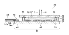
フレキシブル配線基板が配置された電気光学装置の一実施形態について図4及び図5を用いて説明する。図4は、フレキシブル配線基板が配置された電気光学装置の構造を示す模式側断面図である。図5は、フレキシブル配線基板が配置された電気光学装置の構造を示す模式平面図である。本実施形態が第1の実施形態と異なるところは、電気光学装置が液晶表示装置の1種類であるLCOS(Liquid Crystal On Silicon)を備える点にある。尚、第1の実施形態と同じ点については説明を省略する。
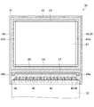
電気光学装置が配置された電子機器であるHMD(Head Mounted Display)の一実施形態について図6を用いて説明する。図6は、HMDの光学系の構造を示す模式平面図である。図6には説明のため使用者の左眼及び右眼を図示する。
前記第1の実施形態では、絶縁部材18は感光性樹脂材料を含んでいた。絶縁部材18は感光性樹脂材料の代わりに熱硬化性の樹脂材料を含んでもよい。光51を当て難いときにも絶縁部材18を加熱して硬化させることができる。
前記第1の実施形態では絶縁部材18はソルダーレジストを含んでいた。絶縁部材18はソルダーレジストを含まない樹脂材料でも良い。塗布し易い樹脂材料を用いても良い。
前記第1の実施形態では第2保護シート17はポリイミドを含む樹脂フィルムで形成されていた。第2保護シート17はポリイミド以外を含む樹脂フィルムで形成されても良い。第2保護シート17は耐熱性を要求されないので、入手し易い樹脂材料を用いても良い。
前記第4の実施形態では、電気光学装置66及び電気光学装置75に第1の実施形態における電気光学装置1を用いた。電気光学装置66及び電気光学装置75に第2の実施形態における電気光学装置25を用いても良い。電気光学装置66及び電気光学装置75に第3の実施形態における電気光学装置30と光源とを組み合わせて用いても良い。電気光学装置30はフレキシブル配線基板32が液晶パネル用基板34の厚み方向に曲がるときにも、第2保護シート17が液晶パネル用基板34と重なってしまい、接続不良となることを防止できる。従って、HMD60はフレキシブル配線基板32が液晶パネル用基板34の厚み方向に曲がるときにも、接続不良となることを防止できる電気光学装置30を備えた機器とすることができる。
前記第4の実施形態では、電気光学装置1を備える電子機器の例としてHMD60を示した。他の電子機器に電気光学装置1、電気光学装置25または電気光学装置30を用いても良い。例えば、投射型表示装置、投射型のHUD(Head−Up Display)、携帯電話機、情報携帯端末、PDA(PersonalDigitalAssistants)、デジタルカメラ、液晶テレビ、カーナビゲーション装置、テレビ電話等に電気光学装置1、電気光学装置25または電気光学装置30を用いても良い。このときにも、フレキシブル配線基板3、フレキシブル配線基板26またはフレキシブル配線基板32が厚み方向に曲がるときにも、接続不良となることを防止できる。
Claims (10)
- 可撓性を有する基材と、
前記基材上に配置される配線と、
前記配線を覆う保護部材と、
前記保護部材から露出した前記配線の一部を覆い前記保護部材より薄い絶縁部材と、を備えることを特徴とするフレキシブル配線基板。 - 請求項1に記載のフレキシブル配線基板であって、
前記基材の平面視において前記絶縁部材は前記保護部材と一部が重なることを特徴とするフレキシブル配線基板。 - 請求項2に記載のフレキシブル配線基板であって、
前記絶縁部材は前記保護部材の側面を覆うことを特徴とするフレキシブル配線基板。 - 請求項1〜3のいずれか一項に記載のフレキシブル配線基板であって、
前記絶縁部材は感光性樹脂材料を含むことを特徴とするフレキシブル配線基板。 - 請求項1〜3のいずれか一項に記載のフレキシブル配線基板であって、
前記絶縁部材はソルダーレジストを含むことを特徴とするフレキシブル配線基板。 - 請求項1〜5のいずれか一項に記載のフレキシブル配線基板であって、
複数の端子を備え、前記絶縁部材は前記複数の端子の配列方向に沿って設けられていることを特徴とするフレキシブル配線基板。 - 請求項1〜6のいずれか一項に記載のフレキシブル配線基板であって、
前記保護部材はポリイミドを含むことを特徴とするフレキシブル配線基板。 - 半導体基板と、前記半導体基板の一辺に沿って設けられたパネル側端子と、を有する電気光学パネルと、
請求項1〜7のいずれか一項に記載のフレキシブル配線基板と、を備え、
前記フレキシブル配線基板の配線は前記パネル側端子と電気的に接続されることを特徴とする電気光学装置。 - 請求項8に記載の電気光学装置であって、
前記フレキシブル配線基板が備える絶縁部材は前記半導体基板の側面の角部と接することを特徴とする電気光学装置。 - 請求項8〜9に記載の電気光学装置を備えることを特徴とする電子機器。
Priority Applications (2)
| Application Number | Priority Date | Filing Date | Title |
|---|---|---|---|
| JP2019149680A JP7392321B2 (ja) | 2019-08-19 | 2019-08-19 | 電気光学装置および電子機器 |
| US16/996,149 US11291111B2 (en) | 2019-08-19 | 2020-08-18 | Flexible wiring substrate, electro-optical device, and electronic apparatus |
Applications Claiming Priority (1)
| Application Number | Priority Date | Filing Date | Title |
|---|---|---|---|
| JP2019149680A JP7392321B2 (ja) | 2019-08-19 | 2019-08-19 | 電気光学装置および電子機器 |
Publications (3)
| Publication Number | Publication Date |
|---|---|
| JP2021032934A true JP2021032934A (ja) | 2021-03-01 |
| JP2021032934A5 JP2021032934A5 (ja) | 2022-07-14 |
| JP7392321B2 JP7392321B2 (ja) | 2023-12-06 |
Family
ID=74646238
Family Applications (1)
| Application Number | Title | Priority Date | Filing Date |
|---|---|---|---|
| JP2019149680A Active JP7392321B2 (ja) | 2019-08-19 | 2019-08-19 | 電気光学装置および電子機器 |
Country Status (2)
| Country | Link |
|---|---|
| US (1) | US11291111B2 (ja) |
| JP (1) | JP7392321B2 (ja) |
Families Citing this family (1)
| Publication number | Priority date | Publication date | Assignee | Title |
|---|---|---|---|---|
| JP7427969B2 (ja) * | 2020-01-22 | 2024-02-06 | セイコーエプソン株式会社 | 電気光学装置および電子機器 |
Citations (8)
| Publication number | Priority date | Publication date | Assignee | Title |
|---|---|---|---|---|
| JPH05249481A (ja) * | 1992-03-10 | 1993-09-28 | Toshiba Corp | ヒートシールコネクタ |
| JP2002358026A (ja) * | 2001-03-26 | 2002-12-13 | Sharp Corp | 表示モジュール並びにフレキシブル配線板及びフレキシブル配線板の接続方法 |
| JP2003302914A (ja) * | 2002-04-09 | 2003-10-24 | Sharp Corp | 電子装置 |
| JP2005050971A (ja) * | 2003-07-31 | 2005-02-24 | Optrex Corp | フレキシブル回路基板 |
| JP2005203104A (ja) * | 2004-01-09 | 2005-07-28 | Opnext Japan Inc | 硬質回路基板とフレキシブル基板との接続構造、接続方法及びそれを用いた回路モジュール |
| US20070103632A1 (en) * | 2005-11-07 | 2007-05-10 | Au Optronics Corp. | Liquid crystal display panel module and flexible printed circuit board thereof |
| JP2010212396A (ja) * | 2009-03-10 | 2010-09-24 | Seiko Epson Corp | 電子装置、電気光学装置および基板の接続構造 |
| CN110121234A (zh) * | 2018-02-07 | 2019-08-13 | 易华电子股份有限公司 | 具耐弯折性的软性电路板 |
Family Cites Families (8)
| Publication number | Priority date | Publication date | Assignee | Title |
|---|---|---|---|---|
| JPS60137670A (ja) * | 1983-12-26 | 1985-07-22 | Hitachi Ltd | 感熱ヘツド |
| JP3767154B2 (ja) | 1997-06-17 | 2006-04-19 | セイコーエプソン株式会社 | 電気光学装置用基板、電気光学装置、電子機器及び投写型表示装置 |
| JP2008159749A (ja) | 2006-12-22 | 2008-07-10 | Japan Electronic Materials Corp | フレキシブルプリント配線板固定構造 |
| JP2009212328A (ja) | 2008-03-05 | 2009-09-17 | Epson Imaging Devices Corp | 回路基板、電気光学装置及び電子機器 |
| JP2010165848A (ja) | 2009-01-15 | 2010-07-29 | Kyocera Chemical Corp | 被覆フレキシブル配線板、液晶表示モジュール、および被覆フレキシブル配線板の製造方法 |
| KR102087951B1 (ko) * | 2013-07-25 | 2020-04-16 | 삼성디스플레이 주식회사 | 평판 디스플레이 장치 및 그 제조방법 |
| JP6300029B2 (ja) * | 2014-01-27 | 2018-03-28 | ソニー株式会社 | 撮像素子、製造装置、製造方法 |
| US10727424B2 (en) * | 2017-04-27 | 2020-07-28 | Sharp Kabushiki Kaisha | Flexible display device |
-
2019
- 2019-08-19 JP JP2019149680A patent/JP7392321B2/ja active Active
-
2020
- 2020-08-18 US US16/996,149 patent/US11291111B2/en active Active
Patent Citations (8)
| Publication number | Priority date | Publication date | Assignee | Title |
|---|---|---|---|---|
| JPH05249481A (ja) * | 1992-03-10 | 1993-09-28 | Toshiba Corp | ヒートシールコネクタ |
| JP2002358026A (ja) * | 2001-03-26 | 2002-12-13 | Sharp Corp | 表示モジュール並びにフレキシブル配線板及びフレキシブル配線板の接続方法 |
| JP2003302914A (ja) * | 2002-04-09 | 2003-10-24 | Sharp Corp | 電子装置 |
| JP2005050971A (ja) * | 2003-07-31 | 2005-02-24 | Optrex Corp | フレキシブル回路基板 |
| JP2005203104A (ja) * | 2004-01-09 | 2005-07-28 | Opnext Japan Inc | 硬質回路基板とフレキシブル基板との接続構造、接続方法及びそれを用いた回路モジュール |
| US20070103632A1 (en) * | 2005-11-07 | 2007-05-10 | Au Optronics Corp. | Liquid crystal display panel module and flexible printed circuit board thereof |
| JP2010212396A (ja) * | 2009-03-10 | 2010-09-24 | Seiko Epson Corp | 電子装置、電気光学装置および基板の接続構造 |
| CN110121234A (zh) * | 2018-02-07 | 2019-08-13 | 易华电子股份有限公司 | 具耐弯折性的软性电路板 |
Also Published As
| Publication number | Publication date |
|---|---|
| US11291111B2 (en) | 2022-03-29 |
| US20210059040A1 (en) | 2021-02-25 |
| JP7392321B2 (ja) | 2023-12-06 |
Similar Documents
| Publication | Publication Date | Title |
|---|---|---|
| JP7034235B2 (ja) | 表示装置、ガラス基板およびガラス基板の製造方法 | |
| US8035789B2 (en) | Mounting structure, electro-optical device, input device, method of manufacturing mounting structure, and electronic apparatus | |
| JP6286911B2 (ja) | 実装構造、電気光学装置及び電子機器 | |
| US7593234B2 (en) | Electro-optical device, method of manufacturing electro-optical device, and electronic apparatus | |
| US8319109B2 (en) | Electro-optical device and electronic apparatus | |
| KR101957998B1 (ko) | 표시 패널 및 이의 제조 방법 | |
| JP4321537B2 (ja) | 液晶装置及び液晶装置の製造方法 | |
| CN106886109B (zh) | 显示装置 | |
| KR20140038823A (ko) | 표시 패널 및 이의 제조 방법 | |
| JP2019020448A (ja) | 表示装置 | |
| US10353253B2 (en) | Mounting substrate and display device | |
| JP2006201216A (ja) | 電気光学装置、電気光学装置の製造方法、電子機器 | |
| KR101830242B1 (ko) | 액정표시장치 | |
| KR20040025606A (ko) | 전기 광학 장치 및 전자 기기 | |
| JP7392321B2 (ja) | 電気光学装置および電子機器 | |
| JP4992774B2 (ja) | 電気光学装置及び電子機器 | |
| JP4147857B2 (ja) | 電気光学装置及び電子機器 | |
| JP2019032410A (ja) | 表示装置 | |
| JP2006201215A (ja) | 電気光学装置、電気光学装置の製造方法、電子機器 | |
| JP2006276600A (ja) | 表示装置 | |
| KR101578215B1 (ko) | 백라이트 유닛 및 이를 구비한 액정표시장치 | |
| JP2019179102A (ja) | 電気光学装置及びその製造方法 | |
| CN113823185B (zh) | 电子装置 | |
| JP2006030829A (ja) | 電気光学装置および電子機器 | |
| CN114709245A (zh) | 显示面板及制备方法、显示模组、显示装置 |
Legal Events
| Date | Code | Title | Description |
|---|---|---|---|
| RD07 | Notification of extinguishment of power of attorney |
Free format text: JAPANESE INTERMEDIATE CODE: A7427 Effective date: 20200811 |
|
| RD04 | Notification of resignation of power of attorney |
Free format text: JAPANESE INTERMEDIATE CODE: A7424 Effective date: 20210915 |
|
| RD03 | Notification of appointment of power of attorney |
Free format text: JAPANESE INTERMEDIATE CODE: A7423 Effective date: 20211102 |
|
| A521 | Request for written amendment filed |
Free format text: JAPANESE INTERMEDIATE CODE: A523 Effective date: 20220706 |
|
| A621 | Written request for application examination |
Free format text: JAPANESE INTERMEDIATE CODE: A621 Effective date: 20220706 |
|
| A977 | Report on retrieval |
Free format text: JAPANESE INTERMEDIATE CODE: A971007 Effective date: 20230222 |
|
| A131 | Notification of reasons for refusal |
Free format text: JAPANESE INTERMEDIATE CODE: A131 Effective date: 20230228 |
|
| A521 | Request for written amendment filed |
Free format text: JAPANESE INTERMEDIATE CODE: A523 Effective date: 20230327 |
|
| A131 | Notification of reasons for refusal |
Free format text: JAPANESE INTERMEDIATE CODE: A131 Effective date: 20230613 |
|
| A521 | Request for written amendment filed |
Free format text: JAPANESE INTERMEDIATE CODE: A523 Effective date: 20230712 |
|
| A02 | Decision of refusal |
Free format text: JAPANESE INTERMEDIATE CODE: A02 Effective date: 20230905 |
|
| A521 | Request for written amendment filed |
Free format text: JAPANESE INTERMEDIATE CODE: A523 Effective date: 20230925 |
|
| A911 | Transfer to examiner for re-examination before appeal (zenchi) |
Free format text: JAPANESE INTERMEDIATE CODE: A911 Effective date: 20231005 |
|
| TRDD | Decision of grant or rejection written | ||
| A01 | Written decision to grant a patent or to grant a registration (utility model) |
Free format text: JAPANESE INTERMEDIATE CODE: A01 Effective date: 20231024 |
|
| A61 | First payment of annual fees (during grant procedure) |
Free format text: JAPANESE INTERMEDIATE CODE: A61 Effective date: 20231106 |
|
| R150 | Certificate of patent or registration of utility model |
Ref document number: 7392321 Country of ref document: JP Free format text: JAPANESE INTERMEDIATE CODE: R150 |