JP2019536282A - 欠陥感受性が低減されたパワーモジュール及びその使用 - Google Patents
欠陥感受性が低減されたパワーモジュール及びその使用 Download PDFInfo
- Publication number
- JP2019536282A JP2019536282A JP2019525950A JP2019525950A JP2019536282A JP 2019536282 A JP2019536282 A JP 2019536282A JP 2019525950 A JP2019525950 A JP 2019525950A JP 2019525950 A JP2019525950 A JP 2019525950A JP 2019536282 A JP2019536282 A JP 2019536282A
- Authority
- JP
- Japan
- Prior art keywords
- power module
- functional element
- module according
- carrier substrate
- functional
- Prior art date
- Legal status (The legal status is an assumption and is not a legal conclusion. Google has not performed a legal analysis and makes no representation as to the accuracy of the status listed.)
- Pending
Links
Images

Classifications
-
- H—ELECTRICITY
- H10—SEMICONDUCTOR DEVICES; ELECTRIC SOLID-STATE DEVICES NOT OTHERWISE PROVIDED FOR
- H10H—INORGANIC LIGHT-EMITTING SEMICONDUCTOR DEVICES HAVING POTENTIAL BARRIERS
- H10H20/00—Individual inorganic light-emitting semiconductor devices having potential barriers, e.g. light-emitting diodes [LED]
- H10H20/80—Constructional details
- H10H20/85—Packages
- H10H20/858—Means for heat extraction or cooling
- H10H20/8585—Means for heat extraction or cooling being an interconnection
-
- H—ELECTRICITY
- H05—ELECTRIC TECHNIQUES NOT OTHERWISE PROVIDED FOR
- H05K—PRINTED CIRCUITS; CASINGS OR CONSTRUCTIONAL DETAILS OF ELECTRIC APPARATUS; MANUFACTURE OF ASSEMBLAGES OF ELECTRICAL COMPONENTS
- H05K1/00—Printed circuits
- H05K1/02—Details
- H05K1/0201—Thermal arrangements, e.g. for cooling, heating or preventing overheating
- H05K1/0203—Cooling of mounted components
- H05K1/0204—Cooling of mounted components using means for thermal conduction connection in the thickness direction of the substrate
-
- H—ELECTRICITY
- H05—ELECTRIC TECHNIQUES NOT OTHERWISE PROVIDED FOR
- H05K—PRINTED CIRCUITS; CASINGS OR CONSTRUCTIONAL DETAILS OF ELECTRIC APPARATUS; MANUFACTURE OF ASSEMBLAGES OF ELECTRICAL COMPONENTS
- H05K1/00—Printed circuits
- H05K1/18—Printed circuits structurally associated with non-printed electric components
- H05K1/182—Printed circuits structurally associated with non-printed electric components associated with components mounted in printed circuit boards [PCB], e.g. insert-mounted components [IMC]
- H05K1/183—Printed circuits structurally associated with non-printed electric components associated with components mounted in printed circuit boards [PCB], e.g. insert-mounted components [IMC] associated with components mounted in and supported by recessed areas of the PCBs
-
- H—ELECTRICITY
- H10—SEMICONDUCTOR DEVICES; ELECTRIC SOLID-STATE DEVICES NOT OTHERWISE PROVIDED FOR
- H10W—GENERIC PACKAGES, INTERCONNECTIONS, CONNECTORS OR OTHER CONSTRUCTIONAL DETAILS OF DEVICES COVERED BY CLASS H10
- H10W90/00—Package configurations
-
- H—ELECTRICITY
- H05—ELECTRIC TECHNIQUES NOT OTHERWISE PROVIDED FOR
- H05K—PRINTED CIRCUITS; CASINGS OR CONSTRUCTIONAL DETAILS OF ELECTRIC APPARATUS; MANUFACTURE OF ASSEMBLAGES OF ELECTRICAL COMPONENTS
- H05K1/00—Printed circuits
- H05K1/02—Details
- H05K1/0201—Thermal arrangements, e.g. for cooling, heating or preventing overheating
- H05K1/0203—Cooling of mounted components
- H05K1/0209—External configuration of printed circuit board adapted for heat dissipation, e.g. lay-out of conductors, coatings
-
- H—ELECTRICITY
- H05—ELECTRIC TECHNIQUES NOT OTHERWISE PROVIDED FOR
- H05K—PRINTED CIRCUITS; CASINGS OR CONSTRUCTIONAL DETAILS OF ELECTRIC APPARATUS; MANUFACTURE OF ASSEMBLAGES OF ELECTRICAL COMPONENTS
- H05K1/00—Printed circuits
- H05K1/02—Details
- H05K1/0213—Electrical arrangements not otherwise provided for
- H05K1/0254—High voltage adaptations; Electrical insulation details; Overvoltage or electrostatic discharge protection ; Arrangements for regulating voltages or for using plural voltages
- H05K1/0257—Overvoltage protection
- H05K1/0259—Electrostatic discharge [ESD] protection
-
- H—ELECTRICITY
- H05—ELECTRIC TECHNIQUES NOT OTHERWISE PROVIDED FOR
- H05K—PRINTED CIRCUITS; CASINGS OR CONSTRUCTIONAL DETAILS OF ELECTRIC APPARATUS; MANUFACTURE OF ASSEMBLAGES OF ELECTRICAL COMPONENTS
- H05K2201/00—Indexing scheme relating to printed circuits covered by H05K1/00
- H05K2201/01—Dielectrics
- H05K2201/0183—Dielectric layers
- H05K2201/0187—Dielectric layers with regions of different dielectrics in the same layer, e.g. in a printed capacitor for locally changing the dielectric properties
-
- H—ELECTRICITY
- H05—ELECTRIC TECHNIQUES NOT OTHERWISE PROVIDED FOR
- H05K—PRINTED CIRCUITS; CASINGS OR CONSTRUCTIONAL DETAILS OF ELECTRIC APPARATUS; MANUFACTURE OF ASSEMBLAGES OF ELECTRICAL COMPONENTS
- H05K2201/00—Indexing scheme relating to printed circuits covered by H05K1/00
- H05K2201/07—Electric details
- H05K2201/073—High voltage adaptations
- H05K2201/0738—Use of voltage responsive materials, e.g. voltage switchable dielectric or varistor materials
-
- H—ELECTRICITY
- H05—ELECTRIC TECHNIQUES NOT OTHERWISE PROVIDED FOR
- H05K—PRINTED CIRCUITS; CASINGS OR CONSTRUCTIONAL DETAILS OF ELECTRIC APPARATUS; MANUFACTURE OF ASSEMBLAGES OF ELECTRICAL COMPONENTS
- H05K2201/00—Indexing scheme relating to printed circuits covered by H05K1/00
- H05K2201/10—Details of components or other objects attached to or integrated in a printed circuit board
- H05K2201/10007—Types of components
- H05K2201/10106—Light emitting diode [LED]
-
- H—ELECTRICITY
- H05—ELECTRIC TECHNIQUES NOT OTHERWISE PROVIDED FOR
- H05K—PRINTED CIRCUITS; CASINGS OR CONSTRUCTIONAL DETAILS OF ELECTRIC APPARATUS; MANUFACTURE OF ASSEMBLAGES OF ELECTRICAL COMPONENTS
- H05K2201/00—Indexing scheme relating to printed circuits covered by H05K1/00
- H05K2201/10—Details of components or other objects attached to or integrated in a printed circuit board
- H05K2201/10007—Types of components
- H05K2201/10196—Variable component, e.g. variable resistor
Landscapes
- Engineering & Computer Science (AREA)
- Microelectronics & Electronic Packaging (AREA)
- Led Device Packages (AREA)
- Cooling Or The Like Of Semiconductors Or Solid State Devices (AREA)
- Structure Of Printed Boards (AREA)
Abstract
Description
とりわけ、むしろより冷暗闇でだけ使用されるわけではない(nicht nur in der eher kuehleren Dunkelheit eingesetzt werden)、一般にドープされた半導体材料を有するLEDに基づく昼間走行灯(Tagfahrlichtern)では、改善された熱導出(Waermeabfuhr)で利益を得る。半導体素子のエージングは、指数関数的な温度依存性を有する熱力学的プロセスである。熱負荷の明らかな低下は(Eine deutliche Verringerung der thermischen Belastung)、相応の部品の寿命を倍増させ、欠陥感受性を低減させることができる。
パワーモジュール内の異なる材料は、一般的に異なる熱膨張係数を有し、従って、さらなる措置なくモジュール内に温度勾配が形成されることは、熱的に誘導された機械的応力を生じさせる。
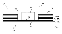
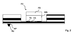
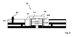
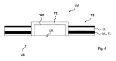
AP コンタクトパッド(Anschlusspad)
BU バンプ接続(Bump-Verbindung)
DK 貫通コンタクト(Durchkontaktierung)
DL 誘電層(dielektrische Lage)
EK 電気コンタクト(elektrischer Kontakt)
EL 電気供給部(elektrische Leitung)
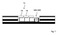
ESD ESD保護(ESD-Schutz)
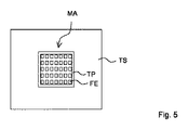
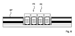
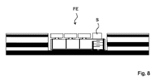
FE 機能素子(Funktionselement)
FS 機能構造(funktionale Struktur)
LM パワーモジュール(Leistungsmodul)
MA マトリックス配置(Matrix-Anordnung)
ML 金属化層(Metallisierungslage)
OS 上面(Oberseite)
S センサー(Sensor)
TA 熱結合(thermische Ankopplung)
TP 温度バッファ(Temperaturpuffer)
TS 担体基板(Traegersubstrat)
TSG 駆動回路(Treiberschaltung)
US 下面(Unterseite)
UV 周囲配線(Umverdrahtung)
VAR バリスタ(Varistor)
WB 熱ブリッジ(Waermebruecke)
Claims (18)
- パワーモジュールであって、
誘電層、金属化層及び凹部を有する担体基板と、
電気的機能素子と、を備え、
前記金属化層において、電気供給部が構造化されており、
前記機能素子は前記電気供給部と接続されており、
前記機能素子は前記凹部内に配置されており、
前記機能素子は、前記担体基板よりも高い熱伝導率を有する熱ブリッジを備えている、
パワーモジュール。 - 前記熱ブリッジは、作動中に生成された熱を前記パワーモジュールの下面に導出するために設けられている、
請求項1記載のパワーモジュール。 - 前記熱ブリッジはセラミック材料を含む、
請求項1又は2記載のパワーモジュール。 - 前記熱ブリッジは、
ZnO−Bi、ZnO−Pr、AlN、Al2O3、SiCから選択された材料を含む又はのみから成る、
請求項1乃至3いずれか1項記載のパワーモジュール。 - 前記熱ブリッジは、前記誘電層と前記金属化層とを有する多層構造を有する、
請求項1乃至4いずれか1項記載のパワーモジュール。 - 前記熱ブリッジは、ESD保護素子を有する、
請求項1乃至5いずれか1項記載のパワーモジュール。 - 前記熱ブリッジはバリスタを有する、
請求項1乃至6いずれか1項記載のパワーモジュール。 - 前記機能素子は、光を放出するように励起可能である機能的構造を有する、
請求項1乃至7いずれか1項記載のパワーモジュール。 - 前記担体基板及び/又は機能素子は垂直方向の貫通コンタクトを有する、
請求項1乃至8いずれか1項記載のパワーモジュール。 - 前記電気供給部と前記機能素子との間の電気的接続は、熱膨張に関して補償されている、
請求項1乃至9いずれか1項記載のパワーモジュール。 - 前記機能素子の下面及び前記凹部の上面の導電性構造は、同一材料から形成されている、
請求項1乃至10いずれか1項記載のパワーモジュール。 - 前記パワーモジュールは、
温度バッファによって充填されているスリットをさらに備え、
前記温度バッファは前記スリットと同一の温度膨張係数を有する、
請求項1乃至11いずれか1項記載のパワーモジュール。 - 前記機能素子を駆動制御するための駆動回路をさらに備え、
前記駆動回路は、前記担体基板上若しくは内に、又は、前記機能素子内に配置されている、
請求項1乃至12いずれか1項記載のパワーモジュール。 - 前記担体基板上若しくは内に、又は、前記機能素子内に配置されているセンサーをさらに備える、
請求項1乃至13いずれか1項記載のパワーモジュール。 - 前記凹部内に規則的な配置で位置決めされた多数の機能素子を有する、
請求項1乃至14いずれか1項記載のパワーモジュール。 - LEDマトリックスモジュールである、
請求項1乃至15いずれか1項記載のパワーモジュール。 - 前記誘電層は、
セラミック材料を含むか、若しくは、セラミック材料のみから成るか、
有機材料を含むか、若しくは、有機材料のみから成るか、又は、
ガラスを含むか、若しくは、ガラスのみから成る、
請求項1乃至16いずれか1項記載のパワーモジュール。 - 車両の照明手段としての請求項1乃至17いずれか1項記載のパワーモジュールの使用。
Applications Claiming Priority (3)
| Application Number | Priority Date | Filing Date | Title |
|---|---|---|---|
| DE102016122014.0 | 2016-11-16 | ||
| DE102016122014.0A DE102016122014A1 (de) | 2016-11-16 | 2016-11-16 | Leistungsmodul mit verringerter Defektanfälligkeit und Verwendung desselben |
| PCT/EP2017/077010 WO2018091230A1 (de) | 2016-11-16 | 2017-10-23 | Leistungsmodul mit verringerter defektanfälligkeit und verwendung desselben |
Publications (1)
| Publication Number | Publication Date |
|---|---|
| JP2019536282A true JP2019536282A (ja) | 2019-12-12 |
Family
ID=60186274
Family Applications (1)
| Application Number | Title | Priority Date | Filing Date |
|---|---|---|---|
| JP2019525950A Pending JP2019536282A (ja) | 2016-11-16 | 2017-10-23 | 欠陥感受性が低減されたパワーモジュール及びその使用 |
Country Status (7)
| Country | Link |
|---|---|
| US (1) | US20190305205A1 (ja) |
| EP (1) | EP3542399B1 (ja) |
| JP (1) | JP2019536282A (ja) |
| CN (1) | CN110140210B (ja) |
| DE (1) | DE102016122014A1 (ja) |
| TW (1) | TWI759338B (ja) |
| WO (1) | WO2018091230A1 (ja) |
Cited By (1)
| Publication number | Priority date | Publication date | Assignee | Title |
|---|---|---|---|---|
| JP2022533469A (ja) * | 2019-07-09 | 2022-07-22 | ヒタチ・エナジー・スウィツァーランド・アクチェンゲゼルシャフト | 集積サージアレスタを有するパワー半導体モジュール |
Families Citing this family (12)
| Publication number | Priority date | Publication date | Assignee | Title |
|---|---|---|---|---|
| US11626448B2 (en) | 2019-03-29 | 2023-04-11 | Lumileds Llc | Fan-out light-emitting diode (LED) device substrate with embedded backplane, lighting system and method of manufacture |
| US11621173B2 (en) | 2019-11-19 | 2023-04-04 | Lumileds Llc | Fan out structure for light-emitting diode (LED) device and lighting system |
| US11777066B2 (en) * | 2019-12-27 | 2023-10-03 | Lumileds Llc | Flipchip interconnected light-emitting diode package assembly |
| US11664347B2 (en) | 2020-01-07 | 2023-05-30 | Lumileds Llc | Ceramic carrier and build up carrier for light-emitting diode (LED) array |
| DE102020100742B4 (de) * | 2020-01-14 | 2024-11-28 | Marelli Automotive Lighting Reutlingen (Germany) GmbH | Lichtmodul, Beleuchtungseinrichtung und Kraftfahrzeug |
| US11476217B2 (en) | 2020-03-10 | 2022-10-18 | Lumileds Llc | Method of manufacturing an augmented LED array assembly |
| US11990872B2 (en) * | 2020-04-17 | 2024-05-21 | Nxp Usa, Inc. | Power amplifier modules including topside cooling interfaces and methods for the fabrication thereof |
| US11990384B2 (en) | 2020-04-17 | 2024-05-21 | Nxp Usa, Inc. | Amplifier modules with power transistor die and peripheral ground connections |
| TWI792356B (zh) * | 2021-06-17 | 2023-02-11 | 大陸商慶鼎精密電子(淮安)有限公司 | 電路板元件及電路板元件的製作方法 |
| CN116158200A (zh) | 2021-06-17 | 2023-05-23 | 庆鼎精密电子(淮安)有限公司 | 电路板组件及电路板组件的制作方法 |
| DE102021123731A1 (de) | 2021-09-14 | 2023-03-16 | TDK Europe GmbH | Elektrisches Bauteil mit verbesserter Kühlung und entsprechendes Modul |
| US12402240B2 (en) * | 2023-04-06 | 2025-08-26 | Wolfspeed, Inc. | Silicon carbide thermal bridge integrated on a low thermal conductivity substrate and processes implementing the same |
Citations (8)
| Publication number | Priority date | Publication date | Assignee | Title |
|---|---|---|---|---|
| JP2001036197A (ja) * | 1999-07-16 | 2001-02-09 | Canon Inc | 光電子集積素子、その駆動方法、該素子を用いた光配線方式、該素子を有する演算処理装置 |
| JP2007227737A (ja) * | 2006-02-24 | 2007-09-06 | Kyocera Corp | 発光素子用配線基板ならびに発光装置 |
| US20100288536A1 (en) * | 2009-05-15 | 2010-11-18 | High Conduction Scientific Co., Ltd. | Ceramic circuit board and method of making the same |
| JP2011524082A (ja) * | 2008-05-21 | 2011-08-25 | エプコス アクチエンゲゼルシャフト | バリスタおよび半導体構成要素を備える電気的構成要素アセンブリ |
| US20120241810A1 (en) * | 2010-11-30 | 2012-09-27 | Zheng Wang | Printing circuit board with micro-radiators |
| JP2012227454A (ja) * | 2011-04-22 | 2012-11-15 | Sanyo Electric Co Ltd | 発光装置用パッケージ及びそれを用いた発光装置 |
| CN103999210A (zh) * | 2011-12-22 | 2014-08-20 | 京瓷株式会社 | 布线基板以及电子装置 |
| JP2016503968A (ja) * | 2013-01-10 | 2016-02-08 | モレックス エルエルシー | Ledアセンブリ |
Family Cites Families (12)
| Publication number | Priority date | Publication date | Assignee | Title |
|---|---|---|---|---|
| DE10316136A1 (de) * | 2003-04-09 | 2004-11-18 | Ixys Semiconductor Gmbh | Gekapselte Leistungshalbleiteranordnung |
| DE102005033709B4 (de) | 2005-03-16 | 2021-12-16 | OSRAM Opto Semiconductors Gesellschaft mit beschränkter Haftung | Lichtemittierendes Modul |
| DE102005054955A1 (de) | 2005-08-31 | 2007-04-26 | Osram Opto Semiconductors Gmbh | Lichtemittierendes Modul, insbesondere zur Verwendung in einem optischen Projektionsgerät und optisches Projektionsgerät |
| DE102008024479A1 (de) * | 2008-05-21 | 2009-12-03 | Epcos Ag | Elektrische Bauelementanordnung |
| CN102593317B (zh) * | 2011-12-20 | 2014-12-24 | 西安炬光科技有限公司 | 一种高功率高亮度led光源封装结构及其封装方法 |
| DE102012104494A1 (de) * | 2012-05-24 | 2013-11-28 | Epcos Ag | Leuchtdiodenvorrichtung |
| JP2014003260A (ja) * | 2012-06-21 | 2014-01-09 | Sumitomo Electric Printed Circuit Inc | プリント配線板、プリント配線板集合体、プリント配線板の製造方法及び照明装置。 |
| DE102012111458B4 (de) * | 2012-11-27 | 2022-12-08 | Tdk Electronics Ag | Halbleitervorrichtung |
| DE102013201775A1 (de) * | 2013-02-04 | 2014-08-07 | Osram Gmbh | Beleuchtungsmodul und Verfahren zur Herstellung eines Beleuchtungsmoduls |
| DE102014115375A1 (de) * | 2014-08-08 | 2016-02-11 | Epcos Ag | Träger für eine LED |
| CN105789197B (zh) * | 2014-12-25 | 2019-03-15 | 日月光半导体制造股份有限公司 | 光学模块、其制造方法以及具有光学模块的电子装置 |
| US9646957B2 (en) * | 2015-01-14 | 2017-05-09 | Everlight Electronics Co., Ltd. | LED packaging structure having stacked arrangement of protection element and LED chip |
-
2016
- 2016-11-16 DE DE102016122014.0A patent/DE102016122014A1/de not_active Withdrawn
-
2017
- 2017-10-12 TW TW106134899A patent/TWI759338B/zh active
- 2017-10-23 WO PCT/EP2017/077010 patent/WO2018091230A1/de not_active Ceased
- 2017-10-23 US US16/347,166 patent/US20190305205A1/en not_active Abandoned
- 2017-10-23 JP JP2019525950A patent/JP2019536282A/ja active Pending
- 2017-10-23 EP EP17791045.2A patent/EP3542399B1/de active Active
- 2017-10-23 CN CN201780071099.6A patent/CN110140210B/zh active Active
Patent Citations (8)
| Publication number | Priority date | Publication date | Assignee | Title |
|---|---|---|---|---|
| JP2001036197A (ja) * | 1999-07-16 | 2001-02-09 | Canon Inc | 光電子集積素子、その駆動方法、該素子を用いた光配線方式、該素子を有する演算処理装置 |
| JP2007227737A (ja) * | 2006-02-24 | 2007-09-06 | Kyocera Corp | 発光素子用配線基板ならびに発光装置 |
| JP2011524082A (ja) * | 2008-05-21 | 2011-08-25 | エプコス アクチエンゲゼルシャフト | バリスタおよび半導体構成要素を備える電気的構成要素アセンブリ |
| US20100288536A1 (en) * | 2009-05-15 | 2010-11-18 | High Conduction Scientific Co., Ltd. | Ceramic circuit board and method of making the same |
| US20120241810A1 (en) * | 2010-11-30 | 2012-09-27 | Zheng Wang | Printing circuit board with micro-radiators |
| JP2012227454A (ja) * | 2011-04-22 | 2012-11-15 | Sanyo Electric Co Ltd | 発光装置用パッケージ及びそれを用いた発光装置 |
| CN103999210A (zh) * | 2011-12-22 | 2014-08-20 | 京瓷株式会社 | 布线基板以及电子装置 |
| JP2016503968A (ja) * | 2013-01-10 | 2016-02-08 | モレックス エルエルシー | Ledアセンブリ |
Cited By (3)
| Publication number | Priority date | Publication date | Assignee | Title |
|---|---|---|---|---|
| JP2022533469A (ja) * | 2019-07-09 | 2022-07-22 | ヒタチ・エナジー・スウィツァーランド・アクチェンゲゼルシャフト | 集積サージアレスタを有するパワー半導体モジュール |
| JP7142183B2 (ja) | 2019-07-09 | 2022-09-26 | ヒタチ・エナジー・スウィツァーランド・アクチェンゲゼルシャフト | 集積サージアレスタを有するパワー半導体モジュール |
| US11495551B2 (en) | 2019-07-09 | 2022-11-08 | Hitachi Energy Switzerland Ag | Power semiconductor module with integrated surge arrester |
Also Published As
| Publication number | Publication date |
|---|---|
| EP3542399A1 (de) | 2019-09-25 |
| TWI759338B (zh) | 2022-04-01 |
| TW201820559A (zh) | 2018-06-01 |
| WO2018091230A1 (de) | 2018-05-24 |
| CN110140210A (zh) | 2019-08-16 |
| DE102016122014A1 (de) | 2018-05-17 |
| CN110140210B (zh) | 2023-10-24 |
| US20190305205A1 (en) | 2019-10-03 |
| EP3542399B1 (de) | 2023-03-08 |
Similar Documents
| Publication | Publication Date | Title |
|---|---|---|
| JP2019536282A (ja) | 欠陥感受性が低減されたパワーモジュール及びその使用 | |
| US8610146B2 (en) | Light emitting diode package and method of manufacturing the same | |
| TWI512915B (zh) | 電子元件組裝架構 | |
| US7872869B2 (en) | Electronic chip module | |
| US8441121B2 (en) | Package carrier and manufacturing method thereof | |
| TWI427761B (zh) | 電子元件組裝架構 | |
| US7253449B2 (en) | Light source module of light emitting diode | |
| US7863639B2 (en) | Light-emitting diode lamp with low thermal resistance | |
| US9349930B2 (en) | LED module and lighting assembly | |
| JP2013522893A (ja) | Ledで使用するためのフィルムシステム | |
| JP2012033662A (ja) | 発光装置及び照明装置 | |
| JP4913099B2 (ja) | 発光装置 | |
| KR101529364B1 (ko) | 배리스터 및 반도체 소자를 포함하는 전기 소자 장치 | |
| US9860990B1 (en) | Circuit board structure with chips embedded therein and manufacturing method thereof | |
| EP3669396B1 (en) | Led module | |
| US8373195B2 (en) | Light-emitting diode lamp with low thermal resistance | |
| KR20100120006A (ko) | 전력 모듈 패키지 | |
| US20100044727A1 (en) | Led package structure | |
| US20160315240A1 (en) | Mounting assembly and lighting device | |
| US20070176182A1 (en) | Structure for integrating LED circuit onto heat-dissipation substrate | |
| JP2006073699A (ja) | 発光素子収納用パッケージ | |
| KR101432372B1 (ko) | 방열 기판 및 방열 기판 제조 방법 | |
| CN105789153A (zh) | 发光装置 | |
| KR101443967B1 (ko) | 방열 기판 및 방열 기판 제조 방법 | |
| KR101237685B1 (ko) | 방열 기판 및 그 제조방법 |
Legal Events
| Date | Code | Title | Description |
|---|---|---|---|
| A621 | Written request for application examination |
Free format text: JAPANESE INTERMEDIATE CODE: A621 Effective date: 20190709 |
|
| A977 | Report on retrieval |
Free format text: JAPANESE INTERMEDIATE CODE: A971007 Effective date: 20200819 |
|
| A131 | Notification of reasons for refusal |
Free format text: JAPANESE INTERMEDIATE CODE: A131 Effective date: 20200825 |
|
| A521 | Request for written amendment filed |
Free format text: JAPANESE INTERMEDIATE CODE: A523 Effective date: 20201124 |
|
| A131 | Notification of reasons for refusal |
Free format text: JAPANESE INTERMEDIATE CODE: A131 Effective date: 20210105 |
|
| A601 | Written request for extension of time |
Free format text: JAPANESE INTERMEDIATE CODE: A601 Effective date: 20210405 |
|
| A521 | Request for written amendment filed |
Free format text: JAPANESE INTERMEDIATE CODE: A523 Effective date: 20210416 |
|
| A02 | Decision of refusal |
Free format text: JAPANESE INTERMEDIATE CODE: A02 Effective date: 20210601 |