JP2019536282A - Power module with reduced defect sensitivity and use thereof - Google Patents
Power module with reduced defect sensitivity and use thereof Download PDFInfo
- Publication number
- JP2019536282A JP2019536282A JP2019525950A JP2019525950A JP2019536282A JP 2019536282 A JP2019536282 A JP 2019536282A JP 2019525950 A JP2019525950 A JP 2019525950A JP 2019525950 A JP2019525950 A JP 2019525950A JP 2019536282 A JP2019536282 A JP 2019536282A
- Authority
- JP
- Japan
- Prior art keywords
- power module
- functional element
- module according
- carrier substrate
- functional
- Prior art date
- Legal status (The legal status is an assumption and is not a legal conclusion. Google has not performed a legal analysis and makes no representation as to the accuracy of the status listed.)
- Pending
Links
Images

Classifications
-
- H—ELECTRICITY
- H10—SEMICONDUCTOR DEVICES; ELECTRIC SOLID-STATE DEVICES NOT OTHERWISE PROVIDED FOR
- H10H—INORGANIC LIGHT-EMITTING SEMICONDUCTOR DEVICES HAVING POTENTIAL BARRIERS
- H10H20/00—Individual inorganic light-emitting semiconductor devices having potential barriers, e.g. light-emitting diodes [LED]
- H10H20/80—Constructional details
- H10H20/85—Packages
- H10H20/858—Means for heat extraction or cooling
- H10H20/8585—Means for heat extraction or cooling being an interconnection
-
- H—ELECTRICITY
- H05—ELECTRIC TECHNIQUES NOT OTHERWISE PROVIDED FOR
- H05K—PRINTED CIRCUITS; CASINGS OR CONSTRUCTIONAL DETAILS OF ELECTRIC APPARATUS; MANUFACTURE OF ASSEMBLAGES OF ELECTRICAL COMPONENTS
- H05K1/00—Printed circuits
- H05K1/02—Details
- H05K1/0201—Thermal arrangements, e.g. for cooling, heating or preventing overheating
- H05K1/0203—Cooling of mounted components
- H05K1/0204—Cooling of mounted components using means for thermal conduction connection in the thickness direction of the substrate
-
- H—ELECTRICITY
- H05—ELECTRIC TECHNIQUES NOT OTHERWISE PROVIDED FOR
- H05K—PRINTED CIRCUITS; CASINGS OR CONSTRUCTIONAL DETAILS OF ELECTRIC APPARATUS; MANUFACTURE OF ASSEMBLAGES OF ELECTRICAL COMPONENTS
- H05K1/00—Printed circuits
- H05K1/18—Printed circuits structurally associated with non-printed electric components
- H05K1/182—Printed circuits structurally associated with non-printed electric components associated with components mounted in printed circuit boards [PCB], e.g. insert-mounted components [IMC]
- H05K1/183—Printed circuits structurally associated with non-printed electric components associated with components mounted in printed circuit boards [PCB], e.g. insert-mounted components [IMC] associated with components mounted in and supported by recessed areas of the PCBs
-
- H—ELECTRICITY
- H10—SEMICONDUCTOR DEVICES; ELECTRIC SOLID-STATE DEVICES NOT OTHERWISE PROVIDED FOR
- H10W—GENERIC PACKAGES, INTERCONNECTIONS, CONNECTORS OR OTHER CONSTRUCTIONAL DETAILS OF DEVICES COVERED BY CLASS H10
- H10W90/00—Package configurations
-
- H—ELECTRICITY
- H05—ELECTRIC TECHNIQUES NOT OTHERWISE PROVIDED FOR
- H05K—PRINTED CIRCUITS; CASINGS OR CONSTRUCTIONAL DETAILS OF ELECTRIC APPARATUS; MANUFACTURE OF ASSEMBLAGES OF ELECTRICAL COMPONENTS
- H05K1/00—Printed circuits
- H05K1/02—Details
- H05K1/0201—Thermal arrangements, e.g. for cooling, heating or preventing overheating
- H05K1/0203—Cooling of mounted components
- H05K1/0209—External configuration of printed circuit board adapted for heat dissipation, e.g. lay-out of conductors, coatings
-
- H—ELECTRICITY
- H05—ELECTRIC TECHNIQUES NOT OTHERWISE PROVIDED FOR
- H05K—PRINTED CIRCUITS; CASINGS OR CONSTRUCTIONAL DETAILS OF ELECTRIC APPARATUS; MANUFACTURE OF ASSEMBLAGES OF ELECTRICAL COMPONENTS
- H05K1/00—Printed circuits
- H05K1/02—Details
- H05K1/0213—Electrical arrangements not otherwise provided for
- H05K1/0254—High voltage adaptations; Electrical insulation details; Overvoltage or electrostatic discharge protection ; Arrangements for regulating voltages or for using plural voltages
- H05K1/0257—Overvoltage protection
- H05K1/0259—Electrostatic discharge [ESD] protection
-
- H—ELECTRICITY
- H05—ELECTRIC TECHNIQUES NOT OTHERWISE PROVIDED FOR
- H05K—PRINTED CIRCUITS; CASINGS OR CONSTRUCTIONAL DETAILS OF ELECTRIC APPARATUS; MANUFACTURE OF ASSEMBLAGES OF ELECTRICAL COMPONENTS
- H05K2201/00—Indexing scheme relating to printed circuits covered by H05K1/00
- H05K2201/01—Dielectrics
- H05K2201/0183—Dielectric layers
- H05K2201/0187—Dielectric layers with regions of different dielectrics in the same layer, e.g. in a printed capacitor for locally changing the dielectric properties
-
- H—ELECTRICITY
- H05—ELECTRIC TECHNIQUES NOT OTHERWISE PROVIDED FOR
- H05K—PRINTED CIRCUITS; CASINGS OR CONSTRUCTIONAL DETAILS OF ELECTRIC APPARATUS; MANUFACTURE OF ASSEMBLAGES OF ELECTRICAL COMPONENTS
- H05K2201/00—Indexing scheme relating to printed circuits covered by H05K1/00
- H05K2201/07—Electric details
- H05K2201/073—High voltage adaptations
- H05K2201/0738—Use of voltage responsive materials, e.g. voltage switchable dielectric or varistor materials
-
- H—ELECTRICITY
- H05—ELECTRIC TECHNIQUES NOT OTHERWISE PROVIDED FOR
- H05K—PRINTED CIRCUITS; CASINGS OR CONSTRUCTIONAL DETAILS OF ELECTRIC APPARATUS; MANUFACTURE OF ASSEMBLAGES OF ELECTRICAL COMPONENTS
- H05K2201/00—Indexing scheme relating to printed circuits covered by H05K1/00
- H05K2201/10—Details of components or other objects attached to or integrated in a printed circuit board
- H05K2201/10007—Types of components
- H05K2201/10106—Light emitting diode [LED]
-
- H—ELECTRICITY
- H05—ELECTRIC TECHNIQUES NOT OTHERWISE PROVIDED FOR
- H05K—PRINTED CIRCUITS; CASINGS OR CONSTRUCTIONAL DETAILS OF ELECTRIC APPARATUS; MANUFACTURE OF ASSEMBLAGES OF ELECTRICAL COMPONENTS
- H05K2201/00—Indexing scheme relating to printed circuits covered by H05K1/00
- H05K2201/10—Details of components or other objects attached to or integrated in a printed circuit board
- H05K2201/10007—Types of components
- H05K2201/10196—Variable component, e.g. variable resistor
Landscapes
- Engineering & Computer Science (AREA)
- Microelectronics & Electronic Packaging (AREA)
- Led Device Packages (AREA)
- Cooling Or The Like Of Semiconductors Or Solid State Devices (AREA)
- Structure Of Printed Boards (AREA)
Abstract
欠陥感受性が低減されたパワーモジュールを提供する。放散されたエネルギーによって生成された熱は、機能的構造から熱ブリッジを介して担体基板の下面へ導出される。熱抵抗を低減するために、機能素子は担体基板の凹部内に位置する。Provided is a power module having reduced defect susceptibility. The heat generated by the dissipated energy is conducted from the functional structure to the lower surface of the carrier substrate via a thermal bridge. In order to reduce the thermal resistance, the functional elements are located in recesses of the carrier substrate.
Description
本発明は、欠陥感受性が低減されたパワーモジュールに関し、また、かかるモジュールの使用に関する。 The present invention relates to power modules with reduced defect sensitivity and to the use of such modules.
技術的装置において、ますます多くの電気及び電子部品が使用されている。相応にその複雑さも向上しており、従って欠陥可能性の数は増加する。さらに、小型化の傾向は続いており、それによって電気的及び電子的機能の実現のための構造空間はますますより小さくなる。 An increasing number of electrical and electronic components are used in technical equipment. Correspondingly, its complexity has also increased, so the number of possible defects increases. Furthermore, the trend towards miniaturization continues, whereby the structural space for the realization of electrical and electronic functions becomes increasingly smaller.
電気及び電子的機能はしばしば電気モジュールによって実現される。1つのモジュールは一般的に、例えばチップ等の複数の電気的コンポーネントを担体基板上に有する。かかるモジュールは、例えば、文献US2009/0129079A1及びUS2008/0151547A1から公知である。 Electrical and electronic functions are often realized by electrical modules. A module typically has a plurality of electrical components, such as chips, on a carrier substrate. Such modules are known, for example, from the documents US2009 / 0129079A1 and US2008 / 0151547A1.
パワーモジュール(Leistungsmodule)、例えば、自動車の道路照明(ヘッドライトのハイビーム、ロービーム)等の照明手段は、単に電気信号だけを処理するシステムと比較して高電力によって特徴づけられる。相応に排熱も、信号処理モジュールの排熱の何倍にもなる。 Lighting means such as power module (Leistungsmodule), for example, road lighting of automobiles (headlight high beam, low beam) are characterized by high power compared to systems that only process electrical signals. Correspondingly, the exhaust heat is also many times that of the signal processing module.
既知のパワーモジュールの問題は、パワーモジュールの欠陥感受性(die Defektanfaelligkeit)及びパワー性能(Leistungsfaehigkeit)の熱的制限である。 A known power module problem is the thermal limitation of the power module (die Defektanfaelligkeit) and power performance (Leistungsfaehigkeit).
従って、小型化への継続的な傾向に従い、より小さな寸法を可能にする、低減された欠陥感受性と、より高いパワー耐性(Leistungsfestigkeit)及びより高いパワー性能とを有するパワーモジュールへの要望がある。 Accordingly, there is a need for a power module that has reduced defect susceptibility, higher power tolerance (Leistungsfestigkeit), and higher power performance that allows for smaller dimensions following a continuing trend toward miniaturization.
この課題は独立請求項1によるパワーモジュールによって解決される。従属請求項は、本発明の有利な形態を提供する。 This problem is solved by a power module according to independent claim 1. The dependent claims provide advantageous forms of the invention.
パワーモジュールは、誘電層と金属化層とを有する担体基板を備える。担体基板はさらに凹部を有する。パワーモジュールはさらに電気的機能素子を有する。担体基板の金属化層において電気配線が構造化される。機能素子は、電気配線と接続されている。機能素子はさらに、担体基板の凹部内に配置されており、担体基板よりも高い熱伝導性を有する熱ブリッジを備える。 The power module includes a carrier substrate having a dielectric layer and a metallized layer. The carrier substrate further has a recess. The power module further has an electrical functional element. Electrical wiring is structured in the metallization layer of the carrier substrate. The functional element is connected to the electrical wiring. The functional element further comprises a thermal bridge which is arranged in the recess of the carrier substrate and has a higher thermal conductivity than the carrier substrate.
凹部は、担体基板を貫通する開口であることができ、従って凹部は担体基板の両面からアクセス可能である。あるいは、凹部は、担体基板を貫通しない、めくら孔の形態の窪みであり得る。そうすると、凹部は担体基板の上面からだけアクセス可能である。後者の場合、凹部は、担体基板の上面によって形成される下面を有する。 The recess can be an opening through the carrier substrate, so that the recess is accessible from both sides of the carrier substrate. Alternatively, the recess can be a depression in the form of a blind hole that does not penetrate the carrier substrate. The recess is then accessible only from the top surface of the carrier substrate. In the latter case, the recess has a lower surface formed by the upper surface of the carrier substrate.
1つの誘電層及び1つの金属化層に加えて、担体基板は、1つ以上のさらなる誘電層及び1つ以上のさらなる金属化層有することができる。誘電層は金属化層を分離する。金属化層において、電気的構造、例えば、信号配線、電力配線、容量、インダクタンス又は抵抗素子等の回路素子が構造化されることができる。 In addition to one dielectric layer and one metallization layer, the carrier substrate can have one or more further dielectric layers and one or more further metallization layers. The dielectric layer separates the metallization layer. In the metallized layer, an electrical structure, for example, a circuit element such as a signal wiring, a power wiring, a capacitor, an inductance, or a resistance element can be structured.
機能素子は、電気的又は電子的パワー素子であり、動作中に比較的高い電力を変換し、相応に高いエネルギー量を放散する(dissipiert)。機能素子は従って動作中に熱源となる。機能素子として、特に高出力LED(LED=Light Emitting Diode=発光ダイオード)のための構造を有する素子が考慮される。 A functional element is an electrical or electronic power element that converts relatively high power during operation and dissipates a correspondingly high amount of energy. The functional element thus becomes a heat source during operation. As the functional element, an element having a structure for a high-power LED (LED = Light Emitting Diode = light-emitting diode) is considered.
熱源として機能し、電気エネルギーを部分的に熱に変換する構造に加えて、機能素子は高い熱伝導性を有する熱ブリッジを備える。担体基板上のチップに熱源を有する従来のパワーモジュールと比較して、凹部内への配置によって、それを介して熱が導出されなければならない担体基板の材料は削減される。担体基板よりも高い熱伝導性により、熱の導出が改善された熱ブリッジの付加的な存在によって、機能素子内のエネルギーを放散する構造の熱的負荷が二重に低減される。 In addition to the structure that functions as a heat source and partially converts electrical energy into heat, the functional element comprises a thermal bridge with high thermal conductivity. Compared to a conventional power module having a heat source in the chip on the carrier substrate, the arrangement in the recess reduces the material of the carrier substrate through which heat must be derived. Due to the higher thermal conductivity than the carrier substrate, the additional presence of a thermal bridge with improved heat dissipation doubles the thermal load of the structure that dissipates energy in the functional element.
自動車が使用される温度範囲は非常に広い。
とりわけ、むしろより冷暗闇でだけ使用されるわけではない(nicht nur in der eher kuehleren Dunkelheit eingesetzt werden)、一般にドープされた半導体材料を有するLEDに基づく昼間走行灯(Tagfahrlichtern)では、改善された熱導出(Waermeabfuhr)で利益を得る。半導体素子のエージングは、指数関数的な温度依存性を有する熱力学的プロセスである。熱負荷の明らかな低下は(Eine deutliche Verringerung der thermischen Belastung)、相応の部品の寿命を倍増させ、欠陥感受性を低減させることができる。
The temperature range in which automobiles are used is very wide.
In particular, rather than being used only in the cold and dark (nicht nur in der eher kuehleren Dunkelheit eingesetzt werden), in general daylighted lamps (Tagfahrlichtern) based on LEDs with doped semiconductor materials, improved heat derivation Profit with (Waermeabfuhr). Aging of a semiconductor device is a thermodynamic process having an exponential temperature dependence. The apparent reduction in heat load (Eine deutliche Verringerung der thermischen Belastung) can double the life of the corresponding part and reduce the defect susceptibility.
凹部内への機能素子の配置によって、モジュールの構造高さ(die Bauhoehe)はさらに低減される。 Due to the arrangement of the functional elements in the recesses, the structural height (die Bauhoehe) of the module is further reduced.
逆説的に言えば、欠陥感受性の低下は、構造体積の縮小に起因するものである。 Paradoxically speaking, the reduction in defect susceptibility is due to a reduction in the structure volume.
全体的に、従って、例えば温度に敏感なパワー半導体等の、ハイパワーに好適であるパワーコンポーネント用の、パワーモジュールが提供される。欠陥感受性は低減されている。一般的により低い温度レベルに基づいて、温度変動は低減される。改善された熱導出により、パワー耐性が向上し、相応に電気コンポーネントはより高いパワーにおいて作動することができる。凹部内の機能素子は、凹部の側壁に機械的に固定的に接続されることができ、従って、基板の機械的安定性を原則的に危うくする凹部にもかかわらず、機械的にロバストなモジュールが得られる。寸法、特に構造高さは低減される。より小さい寸法の選択肢によって、相応のモジュール設計の際の自由度の数が高められ、このことはまた、モジュールの作業性を容易にするための措置に対する空間を残す。 Overall, therefore, a power module is provided for power components that are suitable for high power, such as, for example, temperature-sensitive power semiconductors. Defect susceptibility is reduced. Based on generally lower temperature levels, temperature fluctuations are reduced. With improved heat derivation, power tolerance is increased and correspondingly electrical components can operate at higher power. The functional elements in the recesses can be mechanically fixedly connected to the sidewalls of the recesses, and thus mechanically robust modules despite the recesses that in principle compromise the mechanical stability of the substrate Is obtained. Dimensions, especially the structural height, are reduced. The smaller size option increases the number of degrees of freedom in designing the corresponding module, which also leaves room for measures to facilitate the workability of the module.
通常は、過電圧からモジュールを保護するための構造が得られるように熱ブリッジが形成されることができ、熱誘導欠陥に対する欠陥感受性だけでなく、危険な電気インパルスに対する欠陥感受性も低減されることが知られている。 Typically, a thermal bridge can be formed to provide a structure to protect the module from overvoltage, reducing not only the defect susceptibility to thermally induced defects, but also the susceptibility to dangerous electrical impulses. Are known.
熱ブリッジが、動作中に生成された熱、例えば放散した電気エネルギーをパワーモジュールの下面に導出するために設けられていることが相応に可能である。 Correspondingly, a thermal bridge can be provided to extract heat generated during operation, for example dissipated electrical energy, to the underside of the power module.
パワーモジュールは組立プレート上に固定されており、生成された熱は組立プレートを介してモジュールの周辺環境に導出されることができる。 The power module is fixed on the assembly plate, and the generated heat can be conducted to the surrounding environment of the module through the assembly plate.
熱ブリッジがセラミック材料を有する。 The thermal bridge has a ceramic material.
セラミック材料は誘電材料であることができ、機能素子のパワー構造はその周辺環境に対して絶縁されており、さらに、パワーモジュールの下面への良好な温度接続を実現する The ceramic material can be a dielectric material, the power structure of the functional element is insulated from its surrounding environment, and also provides a good temperature connection to the lower surface of the power module
熱ブリッジが、ZnO−Bi(ビスマスドープ酸化亜鉛(mit Bismut dotiertes Zinkoxid))、ZnO−Pr(プラセオジムドープ酸化亜鉛(mit Praseodym dotiertes Zinkoxid))、AlN(窒化アルミニウム(einem Aluminiumnitrid))、Al2O3及びSiC(炭化ケイ素(Siliziumcarbid))から選択された材料を含むか又は材料のみからなることが可能である。 Thermal bridge, ZnO-Bi (Bismuth-doped zinc oxide (mit Bismut dotiertes Zinkoxid)), ZnO-Pr ( praseodymium-doped zinc oxide (mit Praseodym dotiertes Zinkoxid)), AlN ( aluminum nitride (einem Aluminiumnitrid)), Al 2 O 3 And can comprise a material selected from SiC (Siliziumcarbid) or consist only of material.
担体基板は、PCB(PCB=プリント回路基板(Printed Circuit Board))に使用される通常の材料を含み得る。担体基板は、例えば、多層FR4基板(ein Multilayer-FR4-Substrat)であり得る。あるいは担体基板はIMS基板(IMS=絶縁金属基板(Insulated Metal Substrate))であり得る。既知の基板の熱伝導率は、実質的に8W/mK以下に限定されている。ビスマスドープ酸化亜鉛は、20W/mK以上の熱伝導率を有する。プラセオジムドープ酸化亜鉛は、40W/mK以上の熱伝導性を有する。窒化アルミニウムは、100W/mK以上の熱伝導率を有する。つまり、熱が導出されるために通らなければならない質量の減少(der verringerten Masse,durch die Waerme abgefuehrt werden muss)と共に、熱結合が一桁以上改善され得ることを意味する。 The carrier substrate may comprise the usual materials used for PCBs (PCB = Printed Circuit Board). The carrier substrate can be, for example, a multilayer FR4 substrate (ein Multilayer-FR4-Substrat). Alternatively, the carrier substrate can be an IMS substrate (IMS = Insulated Metal Substrate). The thermal conductivity of known substrates is substantially limited to 8 W / mK or less. Bismuth-doped zinc oxide has a thermal conductivity of 20 W / mK or higher. Praseodymium-doped zinc oxide has a thermal conductivity of 40 W / mK or higher. Aluminum nitride has a thermal conductivity of 100 W / mK or more. This means that the thermal coupling can be improved by an order of magnitude or more, along with the reduction in mass that must be passed for heat to be derived (der verringerten Masse, durch die Waerme abgefuehrt werden muss).
熱ブリッジが多層構造を有することが可能である。多層構造は誘電層と金属化層とを有することができる。さらに、この誘電層に加えて、熱ブリッジはさらなる誘電層を有することができる。さらに、金属化層に加えて、熱ブリッジは、さらなる金属化層を有することができる。 It is possible for the thermal bridge to have a multilayer structure. The multilayer structure can have a dielectric layer and a metallization layer. Furthermore, in addition to this dielectric layer, the thermal bridge can have an additional dielectric layer. Furthermore, in addition to the metallization layer, the thermal bridge can have an additional metallization layer.
多層構造の層内において、電気的機能が実現されることができる。有利には、誘電材料及び金属化層の材料は、熱ブリッジ全体を介して最適な熱導出が提供されるように選択される。 In the layers of the multilayer structure, electrical functions can be realized. Advantageously, the dielectric material and the material of the metallization layer are selected so as to provide optimum heat derivation through the entire thermal bridge.
熱ブリッジがESD保護素子(ESD=静電放電(Electro-Static Discharge))を含むことが可能である。 It is possible that the thermal bridge includes an ESD protection element (ESD = Electro-Static Discharge).
ESD保護素子は、故障を起こし得る(schaedlichen)電圧インパルスから機能素子の機能的構造を保護し得る。 The ESD protection element can protect the functional structure of the functional element from voltage impulses that can fail.
さらに、熱ブリッジがバリスタを含むことが可能である。 Further, the thermal bridge can include a varistor.
熱ブリッジは、多層構造を有し、そこでは、上下に配置されて、誘電材料によって分離されている第1電極が構造化されている。第1電極の間では、さらなる金属化層において、第1電極から分離された第2電極面が構造化されている。 The thermal bridge has a multi-layer structure in which a first electrode is arranged one above the other and separated by a dielectric material. Between the first electrodes, a second electrode surface separated from the first electrode is structured in a further metallization layer.
バリスタセラミックの形態の誘電材料は、この場合、電極に印加される電圧に応じた電気抵抗を有する。誘電材料が機能素子の通常の動作電圧において絶縁体を示す間、不所望な過電圧パルスは、このようにして容易に保護電位に、例えば設置電位に、放出されることができる。 The dielectric material in the form of a varistor ceramic in this case has an electrical resistance that depends on the voltage applied to the electrodes. While the dielectric material exhibits an insulator at the normal operating voltage of the functional element, undesired overvoltage pulses can easily be released to the protective potential, for example to the installation potential.
パワーモジュールは、機能素子に加えて、同一の又は類似の構造を有するさらなる付加的な機能素子を備えることができ、同様に凹部内又は付加的な凹部内に配置されることができる。かかる配置によって高い集積度を得ることができる。集積度及び従って集積される機能素子の数が高ければ高いほど、故障確率(Ausfallwahrscheinlichkeit)は高くなる。パワーモジュールが個別の機能素子の故障に基づいて使用できなくなることは望ましくない。上述したようなESD保護の選択肢によって、ハイパワーに使用できる多数の機能素子を有する高集積化部品を得ることができ、それでもなお、故障確率が最小限に抑えられている。機能素子が光を放出するように励起可能である機能的構造を備えることが可能である。 In addition to the functional elements, the power module can comprise further additional functional elements having the same or similar structure and can likewise be arranged in the recesses or in the additional recesses. With this arrangement, a high degree of integration can be obtained. The higher the degree of integration and thus the number of functional elements integrated, the higher the probability of failure (Ausfallwahrscheinlichkeit). It is undesirable for a power module to become unusable based on the failure of an individual functional element. With the ESD protection options as described above, highly integrated components with many functional elements that can be used for high power can be obtained, yet the probability of failure is kept to a minimum. It is possible to provide a functional structure that can be excited so that the functional element emits light.
熱ブリッジが機能的構造を機能素子の下面、例えばパワーモジュールの下面に、熱的に連結する(anbindet)間、機能的構造は、有利には、機能素子の上面に配置される。光を放出するために励起可能な構造は特に、半導体材料に基づくLED構造上にあることができる。なぜなら、かかる半導体構造は、特に過加熱に対して敏感だからである。 While the thermal bridge anbindet the functional structure to the lower surface of the functional element, eg, the lower surface of the power module, the functional structure is advantageously arranged on the upper surface of the functional element. Structures that can be excited to emit light can be in particular on LED structures based on semiconductor materials. This is because such semiconductor structures are particularly sensitive to overheating.
担体基板及び/又は機能素子が垂直貫通コンタクト、所謂ビア、を有することが可能である。垂直貫通コンタクトは、この場合、異なる金属化層又は異なる金属化層内において構造化された回路素子を接続する(verschalten)。かかる貫通コンタクトは、パワーモジュールの全電気接続を単一の面、例えば下面に配置すること可能にする。相応に、機能素子が担体基板への全ての電気接続を下面に有することも可能である。そうすると、凹部内の機能素子は担体基板の1つの層上に配置され、構造化された配線を介して接続されている。 It is possible for the carrier substrate and / or the functional element to have vertical through contacts, so-called vias. The vertical through contacts in this case connect different metallization layers or circuit elements structured in different metallization layers. Such feedthrough contacts allow all electrical connections of the power module to be arranged on a single surface, for example the lower surface. Correspondingly, it is also possible for the functional element to have all electrical connections to the carrier substrate on the underside. If it does so, the functional element in a recessed part will be arrange | positioned on one layer of a support | carrier board | substrate, and will be connected via the structured wiring.
誘電層の間に全面的に形成された金属化層を有する既知のIMS基板は、かかるコンタクトを許容しない。なぜなら、相応に設けられた複数の垂直方向の貫通コンタクトが大面積で形成された金属層によって短絡されるからである。担体基板の上面及び下面の間のコンタクトは、従ってかかる既知の基板において可能ではない。 Known IMS substrates having a metallization layer formed entirely between the dielectric layers do not allow such contacts. This is because a corresponding plurality of vertical through-contacts are short-circuited by a metal layer having a large area. Contact between the upper and lower surfaces of the carrier substrate is therefore not possible with such known substrates.
担体基板の電気配線と機能素子との間の電気接続(eine elektrische Verbindung)が熱膨張を補償することが可能である。 The electrical connection between the electrical wiring of the carrier substrate and the functional element (eine elektrische Verbindung) can compensate for thermal expansion.
パワーモジュールの下面への機能素子の機能的構造の熱接続が改善されている(der verbesserten thermischen Anbindung)にもかかわらず、パワーモジュール内に温度差が生じる可能性がある。
パワーモジュール内の異なる材料は、一般的に異なる熱膨張係数を有し、従って、さらなる措置なくモジュール内に温度勾配が形成されることは、熱的に誘導された機械的応力を生じさせる。
Despite improved thermal connection of the functional structure of the functional element to the underside of the power module (der verbesserten thermischen Anbindung), temperature differences can occur in the power module.
Different materials in the power module generally have different coefficients of thermal expansion, so that the formation of a temperature gradient in the module without further measures creates a thermally induced mechanical stress.
異なる熱膨張を補償することは、それによって、機械的応力の低減と、担体基板と機能素子との間の電気接続にかかる機械的負荷の低減を引き起こす。従って、欠陥感受性が低減されることに加え、機能素子への熱的負荷が低減することと、不所望な電気的インパルスからの保護により欠陥感受性が低減することとは、基板と機能ユニットとの間の接続位置の機械的損傷(mechanischen Schaeden)に対する欠陥感受性をも低減する。 Compensating for different thermal expansions thereby causes a reduction in mechanical stress and a reduction in the mechanical load on the electrical connection between the carrier substrate and the functional element. Therefore, in addition to the reduction in defect sensitivity, the reduction in thermal load on the functional element and the reduction in defect sensitivity due to protection from undesired electrical impulses are the relationship between the substrate and the functional unit. It also reduces the susceptibility of defects to mechanical damage at the connection location between them (mechanischen Schaeden).
機能素子の下面の導電性構造と、凹部の上面の導電構造とに、同一の材料を使用することは、熱膨張の補償に有利な選択肢である。 Using the same material for the conductive structure on the lower surface of the functional element and the conductive structure on the upper surface of the recess is an advantageous option for compensating for thermal expansion.
その際、特に、等方性の温度膨張挙動を示し、その膨張係数の張力(deren Tensor)が、ゼロではない同一の対角要素(Diagonalelemente)のみを有する材料が有利である。 In this case, in particular, a material having an isotropic temperature expansion behavior and having only the same diagonal element whose expansion coefficient tension (deren Tensor) is not zero is advantageous.
従って、例えばバンプ接続等の接続用の凹部内の担体基板の上面と、機能素子の下面とにおいて、それらの間に銅だけ又は銀だけが用いられることが可能である。 Therefore, for example, only copper or only silver can be used between the upper surface of the carrier substrate in the concave portion for connection such as bump connection and the lower surface of the functional element.
さらに、パワーモジュールが温度バッファを含むことが可能である。機能素子は、担体基板のその位置の局所的な上面(die dortige lokale Oberseite)を介して形成される凹部の下面又は底面から垂直方向に、又は、凹部の側壁から水平方向に離間していることができる。相応に、垂直スリットが機能素子の隣りに存在し、又は、水平スリットが機能素子と凹部の「底(Boden)」との間に存在する。スリットは温度バッファの材料によって充填されることができる。水平方向において、機能素子は第1係数を有することができる。担体基板は水平方向において、第1係数とは異なる第2温度膨張係数を有することができる。温度変化の際には、機能素子と凹部の幅は異なる大きさで(stark)変化する。相応にスリットは大きくなり又は小さくなる。温度バッファは、好ましくは、計算上容易に求められる、スリットの「温度膨張係数」に実質的に相応する温度膨張係数を有する。即ち、温度バッファによって、各温度において及び温度変化において、担体基板と機能素子との間の形状結合による接続が与えられ、それによってパワーモジュールの機械的安定性が高められる。特に、スリット及び温度バッファの温度膨張係数は約5ppm/K以下だけ異なることが可能である。 Further, the power module can include a temperature buffer. The functional element is vertically spaced from the bottom or bottom surface of the recess formed via the local top surface (die dortige lokale Oberseite) of the carrier substrate, or horizontally from the sidewall of the recess. Can do. Correspondingly, there is a vertical slit next to the functional element or a horizontal slit between the functional element and the “Boden” of the recess. The slit can be filled with temperature buffer material. In the horizontal direction, the functional element may have a first coefficient. The carrier substrate may have a second temperature expansion coefficient different from the first coefficient in the horizontal direction. When the temperature changes, the widths of the functional element and the recess change with different sizes (stark). Correspondingly, the slit becomes larger or smaller. The temperature buffer preferably has a coefficient of thermal expansion substantially corresponding to the “temperature coefficient of expansion” of the slit, which is easily calculated. That is, the temperature buffer provides a connection by shape coupling between the carrier substrate and the functional element at each temperature and at a temperature change, thereby increasing the mechanical stability of the power module. In particular, the coefficient of thermal expansion of the slit and temperature buffer can differ by about 5 ppm / K or less.
パワーモジュールは、機能素子の駆動制御のための駆動回路を含むことが可能である。駆動回路はその際、担体基板の上方に若しくは上に配置されるか又は担体基板内に集積化されることができる。駆動回路は、機能素子の上方に若しくは上に配置されるか又は機能素子内に集積化されることもできる。 The power module can include a drive circuit for drive control of the functional element. The drive circuit can then be arranged above or on the carrier substrate or integrated in the carrier substrate. The drive circuit can also be arranged above or on the functional element or integrated in the functional element.
パワーモジュールが1つより多い機能素子を有する場合、従って、単一の駆動回路は複数の又は全ての機能素子を駆動制御することができる。あるいは、機能素子ごとに1つの固有の駆動回路が設けられているか、又は、機能素子の異なるグループがあり、各グループについてそれぞれ1つの駆動回路が設けられていることも可能である。 If the power module has more than one functional element, therefore, a single drive circuit can drive and control multiple or all functional elements. Alternatively, one functional drive circuit may be provided for each functional element, or there may be different groups of functional elements, and one drive circuit may be provided for each group.
パワーモジュールはセンサーを含むことが可能である。センサーは担体基板の上方に又は上に配置されるか又は担体基板内に集積化されることができる。センサーが機能素子の上方に又は上に配置されるか又は機能素子内に集積化されることも可能である。 The power module can include a sensor. The sensor can be arranged above or on the carrier substrate or integrated in the carrier substrate. It is also possible that the sensor is arranged above or on the functional element or integrated in the functional element.
センサーは特に温度センサーであることができ、常に、機能素子、担体基板又はパワーモジュール全体の現在の温度レベルを観察し、温度値を駆動回路に転送する。 The sensor can in particular be a temperature sensor, which always observes the current temperature level of the functional element, the carrier substrate or the entire power module and transfers the temperature value to the drive circuit.
駆動回路において、機能素子又は複数の機能素子の活動を外部制御信号に依存して及びセンサーの測定値に依存して、開ループ又は閉ループ制御する回路ロジックが集積化されている。 In the drive circuit, circuit logic is integrated which controls the activity of the functional element or the functional elements depending on the external control signal and on the measured value of the sensor.
パワーモジュールは多数の機能素子を有することが可能である。複数の機能素子は規則的な配置においいて、まとめて1つの凹部内に位置決めされるか、又は個別の凹部内に位置決めされる。機能素子は特に行及び列において、即ち、マトリックス配置において、位置決めされることができる。 The power module can have a large number of functional elements. The plurality of functional elements are positioned in a single recess together in a regular arrangement or in individual recesses. The functional elements can be positioned in particular in rows and columns, i.e. in a matrix arrangement.
相応に、パワーモジュールはLEDマトリックスモジュールであることが可能である。 Correspondingly, the power module can be an LED matrix module.
担体基板の1つ以上の誘電層がセラミック材料を含むか若しくはセラミック材料のみから成るか、又は有機材料を含むか若しくは有機材料のみから成るか、又はガラスを含むか若しくはガラスのみから成ることが可能である。 It is possible that one or more dielectric layers of the carrier substrate comprise a ceramic material or consist solely of a ceramic material, or comprise an organic material or consist only of an organic material, or comprise glass or consist solely of glass It is.
セラミック材料としては、AIN及びAl2O3が考えられる。有機材料としては樹脂が考えられる。ガラスとしては通常のガラスが考えられる。 AIN and Al 2 O 3 are conceivable as ceramic materials. Resin is considered as the organic material. As glass, normal glass can be considered.
担体基板内の誘電材料が配線基板のための標準材料、例えばFR4、であることも可能である。パワーモジュールは、光照明手段として、例えば、ヘッドライトのハイビーム(Fernlicht)、ロービーム(Abblendlicht)若しくは昼間走行灯として、又は方向指示器(ウィンカー)として、使用されることが可能である。 It is also possible that the dielectric material in the carrier substrate is a standard material for the wiring substrate, for example FR4. The power module can be used as a light illuminating means, for example, as a headlight high beam (Fernlicht), low beam (Abblendlicht) or daytime running light, or as a turn indicator (winker).
以下では、パワーモジュールの機能原理と可能な実施形態の選択された詳細が図面を参照して述べられる。 In the following, the functional principle of the power module and selected details of possible embodiments will be described with reference to the drawings.
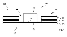
図1は、複数の層を有する担体基板を備えたパワーモジュールの基本的構造を示す。特に、絶縁性材料製の誘電層DLと、電気構造が形成されることができる金属化層MLとを含む。担体基板TSには凹部ANがあり、その中には、機能素子FEを配置することができる。図1は、凹部が、所謂めくら孔形状を有することを示し、従って凹部は底を有する。凹部の底の上には機能素子FEが配置されている。一方にのみ開口した凹部ANを有するパワーモジュールLMにおいては、凹部が開口している側が上面OSである。対向する側は下面である。 FIG. 1 shows the basic structure of a power module comprising a carrier substrate having a plurality of layers. In particular, it includes a dielectric layer DL made of an insulating material and a metallized layer ML on which an electrical structure can be formed. The carrier substrate TS has a recess AN in which the functional element FE can be arranged. FIG. 1 shows that the recess has a so-called blind hole shape, so that the recess has a bottom. A functional element FE is disposed on the bottom of the recess. In the power module LM having the recess AN opened only on one side, the side where the recess is opened is the upper surface OS. The opposite side is the lower surface.
機能素子FEは電気的コンタクトEKを介して、例えば金属化層内に形成された電気供給部ELと接続される。 The functional element FE is connected via an electrical contact EK to, for example, an electrical supply part EL formed in the metallization layer.
機能素子FE内の、特に機能素子FEの上面で形成される熱は、低抵抗を有する機能素子FEを貫通する。この熱をパワーモジュールの下面を介して外部環境に放出できるようにするためには、機能素子が凹部内ではなく担体基板の上面OSに配置されていた場合よりも、凹部ANとしてめくら孔の場合の方が乗り越えられるべき担体基板材料の量が少ない。 The heat formed in the functional element FE, particularly on the upper surface of the functional element FE, penetrates the functional element FE having a low resistance. In order to be able to release this heat to the external environment via the lower surface of the power module, the concave portion AN is a blind hole rather than the functional element being disposed not on the concave portion but on the upper surface OS of the carrier substrate. The amount of carrier substrate material to be overcome is smaller.
相応に、凹部AN領域において担体基板TSの局所的厚さが、凹部の無い領域における局所よりも小さいと有利である。 Correspondingly, it is advantageous if the local thickness of the carrier substrate TS in the recess AN region is smaller than in the region without the recess.
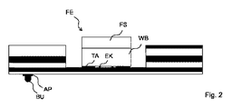
図2は、機能素子FEが2つの上下に配置された領域を有する配置を示す。上部領域は、例えば電気的又は電子的又は光学的機能を実現する機能的構造FSを有する部分を形成する。その下には、上部部分で生成された熱を機能素FEの下面へ、従ってパワーモジュールの下面へと導く熱ブリッジWBが配置されている。 FIG. 2 shows an arrangement in which the functional element FE has two upper and lower regions. The upper region forms, for example, a part having a functional structure FS that realizes an electrical, electronic or optical function. Below that, a thermal bridge WB is arranged which guides the heat generated in the upper part to the lower surface of the functional element FE and thus to the lower surface of the power module.
パワーモジュールの下面への熱の伝達を容易にするために、熱ブリッジWBは熱的結合TAを介して凹部の底と接続されている。熱的結合TAは、例えば導体ペースト又は金属化部によって形成されており、熱抵抗が低減されている。熱的結合TAは、好ましくは低い熱抵抗を有する材料、例えば銅又は銀を含む。 In order to facilitate the transfer of heat to the lower surface of the power module, the thermal bridge WB is connected to the bottom of the recess via a thermal coupling TA. The thermal coupling TA is formed by, for example, a conductor paste or a metallized portion, and the thermal resistance is reduced. The thermal bond TA preferably comprises a material having a low thermal resistance, such as copper or silver.
パワーモジュールの下面には、コンタクトパッドAPが設けられており、例えばUBM(UBM=バンプ下金属化部(Under-Bump Metallization))によって形成されている。かかるコンタクトパッドを介して、パワーモジュールはバンプ接続BUを介して外部環境と連結されることができ、接続されることができる。 A contact pad AP is provided on the lower surface of the power module, and is formed by, for example, UBM (UBM = Under-Bump Metallization). Through such a contact pad, the power module can be connected to and connected to the external environment via a bump connection BU.
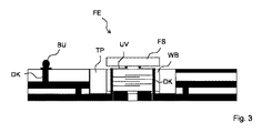
図3は、熱ブリッジWBが多層構造(einen Mehrlagenaufbau)を有するパワーモジュールの詳細を示す。その中では、誘電層及び金属化層が上下に重なり合って配置されている。誘電層の材料が相応に選択されている場合、かかる構造は熱を良好に伝導する。かかる熱ブリッジWBは、熱の導出に加えて、電気的又は電子的機能を提供する。従って、金属化層内に電極を形成することが可能である。電極は、誘電材料を介して垂直方向に上下に分離されている。垂直方向において隣り合う電極は異なるコンタクトに割当られている。誘電材料がバリスタ材料であれば、2つの異なるコンタクトは低電圧に関して互いに絶縁されている。2つの異なるコンタクトに高電圧、例えばESDパルス、が印加されていると、バリスタ材料は低減された電気抵抗を示し、ESDパルスは参照電位に導出されることができる。 FIG. 3 shows details of a power module in which the thermal bridge WB has a multilayer structure (einen Mehrlagenaufbau). Among them, the dielectric layer and the metallized layer are arranged so as to overlap each other. Such a structure conducts heat well if the material of the dielectric layer is selected accordingly. Such a thermal bridge WB provides an electrical or electronic function in addition to heat extraction. Thus, it is possible to form electrodes in the metallization layer. The electrodes are separated vertically by a dielectric material. The electrodes adjacent in the vertical direction are assigned to different contacts. If the dielectric material is a varistor material, the two different contacts are insulated from each other for low voltages. When a high voltage, such as an ESD pulse, is applied to two different contacts, the varistor material exhibits a reduced electrical resistance and the ESD pulse can be derived to a reference potential.
熱ブリッジWBは垂直方向の貫通コンタクトDK(ビア)を有し、これを介して、機能素子の上面の機能的構造FSは構造化された担体基板の金属化部と接続されている。 The thermal bridge WB has a vertical through contact DK (via) through which the functional structure FS on the upper surface of the functional element is connected to the metallization part of the structured carrier substrate.
多層の形態の担体基板にも、貫通コンタクトDKがあり、回路素子又は配線を異なる金属化層に相互に接続する。貫通コンタクトDKを介して、パワーモジュールの全ての外部コンタクトを、パワーモジュールの1つの面上に配置することが可能であり、このことは外部回路環境への集積化を容易にする。 Multi-layered carrier substrates also have through contacts DK that connect circuit elements or wirings to different metallization layers. Via the through contacts DK, all external contacts of the power module can be arranged on one side of the power module, which facilitates integration in the external circuit environment.
機能素子FEの多層構造は、機熱ブリッジの接続コンタクトへの機能的構造の電気的コンタクトを単純化するための付加的な周辺配線UVを有する。 The multilayer structure of the functional element FE has an additional peripheral wiring UV to simplify the electrical contact of the functional structure to the connection contacts of the machine thermal bridge.
水平方向において機能素子FEは凹部の側壁から離間している。この容積は、温度膨張係数を有する温度バッファTPの材料によって充填され、温度膨張係数は、バッファTPの増大又は縮小少がスリットの幅の増大又は縮小と同じになるように選択されている。 In the horizontal direction, the functional element FE is separated from the side wall of the recess. This volume is filled by the material of the temperature buffer TP having a temperature expansion coefficient, and the temperature expansion coefficient is selected so that increasing or decreasing the buffer TP is the same as increasing or decreasing the width of the slit.
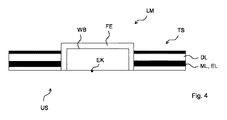
図4は、凹部が担体基板を完全に、基面の全領域において貫通するパワーモジュールの形態を示す。パワーモジュールの全体高さを最大限に低減するために、機能素子は完全に担体基板に埋め込まれている。外部環境への集積化を容易にするために、特に下方への熱排出を容易にするために、機能素子の下面、特にその熱ブリッジWBと、担体基板の下面USと、が面一に整列されており、従って、実質的に平坦なパワーモジュール全体の下面を得ることができる。 FIG. 4 shows a configuration of the power module in which the recess penetrates the carrier substrate completely in the entire area of the base surface. In order to reduce the overall height of the power module to the maximum, the functional element is completely embedded in the carrier substrate. In order to facilitate integration in the external environment, in particular in order to facilitate heat dissipation downward, the lower surface of the functional element, in particular its thermal bridge WB, and the lower surface US of the carrier substrate are aligned flush. Therefore, the lower surface of the entire power module that is substantially flat can be obtained.
機能素子の下面への電気的コンタクトは、パワーモジュールの下面から突出することができる。あるいは、機能素子FEが担体基板に埋め込まれている限り、担体基板の下面は、電気的コンタクトEKと面一になることも可能である。 The electrical contact to the lower surface of the functional element can protrude from the lower surface of the power module. Alternatively, as long as the functional element FE is embedded in the carrier substrate, the lower surface of the carrier substrate can be flush with the electrical contact EK.
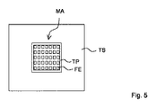
図5は多数の機能素子FEが行と列に整列されたマトリックス配置MAの上面図を示す。 FIG. 5 shows a top view of a matrix arrangement MA in which a number of functional elements FE are arranged in rows and columns.
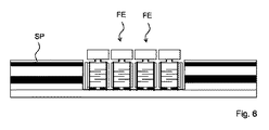
図6は、唯一の凹部が設けられており、その中に多数の機能素子FEが配置されている選択肢を示す。各機能素子FEは、多層構造を有する熱ブリッジと、熱ブリッジの上方の機能的構造とを有する。 FIG. 6 shows an option in which only one recess is provided in which a number of functional elements FE are arranged. Each functional element FE has a thermal bridge having a multilayer structure and a functional structure above the thermal bridge.
担体基盤の最上層は、光を反射するミラーSPであり得る。機能的構造が光源を形成する場合、担体基板のそれ以外の受動的な上面(die ansonsten passive Oberseite)によって吸収される光が少ない場合、パワーモジュールの放出光の全量は高められる。 The top layer of the carrier substrate can be a mirror SP that reflects light. When the functional structure forms a light source, the total amount of light emitted by the power module is increased if less light is absorbed by the other passive upper surface of the carrier substrate.
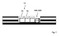
図7は、複数の機能的構造FSが単一の機能素子FE内に設けられる選択肢を示す。機能素子FEの熱ブリッジは、バリスタ材料を有する多層構造を有し、ESD保護機能を提供する。 FIG. 7 shows an option in which a plurality of functional structures FS are provided in a single functional element FE. The thermal bridge of the functional element FE has a multilayer structure with a varistor material and provides an ESD protection function.
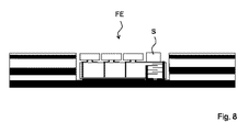
図8は、センサーが機能素子FEの上面上に直接配置される選択肢を示す。あるいは、センサーは機能素子の多層構造内に又は担体基板上に若しくは内に配置されることができる。 FIG. 8 shows an option in which the sensor is arranged directly on the upper surface of the functional element FE. Alternatively, the sensor can be arranged in a multilayer structure of functional elements or on or in a carrier substrate.
図9は、センサーSを担体基板の多層構造の内部に配置する選択肢を示す。対照的に、機能素子FE上には、機能的構造を駆動制御し、その作動方法を閉ループ又は開ループ制御するための(zu steuern oder zu regeln)駆動回路TSGが配置されている。駆動回路TSGはその際、同様に電気的又は電子的に電力コンポーネントを含み得る。熱ブリッジ上への配置はこの場合好ましい。 FIG. 9 shows the option of placing the sensor S inside the multilayer structure of the carrier substrate. In contrast, a drive circuit TSG is arranged on the functional element FE to drive and control the functional structure and to control its operating method in a closed-loop or open-loop manner (zu steuern oder zu regeln). The drive circuit TSG may then include power components as well, electrically or electronically. An arrangement on the thermal bridge is preferred in this case.
パワーモジュール及びパワーモジュールの使用は、記載された技術的特徴及び示された詳細に制限されない。追加の回路素子、追加のコンタクト及び追加の凹部を有するパワーモジュールは同様に保護範囲に含まれる。 The power module and the use of the power module are not limited to the described technical features and details shown. Power modules with additional circuit elements, additional contacts and additional recesses are likewise included in the protection range.
AN 凹部(Ausnehmung)
AP コンタクトパッド(Anschlusspad)
BU バンプ接続(Bump-Verbindung)
DK 貫通コンタクト(Durchkontaktierung)
DL 誘電層(dielektrische Lage)
EK 電気コンタクト(elektrischer Kontakt)
EL 電気供給部(elektrische Leitung)
ESD ESD保護(ESD-Schutz)
FE 機能素子(Funktionselement)
FS 機能構造(funktionale Struktur)
LM パワーモジュール(Leistungsmodul)
MA マトリックス配置(Matrix-Anordnung)
ML 金属化層(Metallisierungslage)
OS 上面(Oberseite)
S センサー(Sensor)
TA 熱結合(thermische Ankopplung)
TP 温度バッファ(Temperaturpuffer)
TS 担体基板(Traegersubstrat)
TSG 駆動回路(Treiberschaltung)
US 下面(Unterseite)
UV 周囲配線(Umverdrahtung)
VAR バリスタ(Varistor)
WB 熱ブリッジ(Waermebruecke)
AN recess (Ausnehmung)
AP contact pad (Anschlusspad)
BU Bump connection (Bump-Verbindung)
DK through contact (Durchkontaktierung)
DL dielectric layer (dielektrische Lage)
EK electrical contact (elektrischer Kontakt)
EL electricity supply (elektrische Leitung)
ESD ESD protection (ESD-Schutz)
FE functional elements
FS functional structure (funktionale Struktur)
LM Power Module (Leistungsmodul)
MA matrix arrangement (Matrix-Anordnung)
ML Metallizing layers (Metallisierungslage)
OS top surface (Oberseite)
S sensor
TA thermal bonding (thermische Ankopplung)
TP temperature buffer (Temperaturpuffer)
TS carrier substrate (Traegersubstrat)
TSG drive circuit (Treiberschaltung)
US bottom surface (Unterseite)
UV ambient wiring (Umverdrahtung)
VAR Varistor
WB Thermal Bridge (Waermebruecke)
Claims (18)
誘電層、金属化層及び凹部を有する担体基板と、
電気的機能素子と、を備え、
前記金属化層において、電気供給部が構造化されており、
前記機能素子は前記電気供給部と接続されており、
前記機能素子は前記凹部内に配置されており、
前記機能素子は、前記担体基板よりも高い熱伝導率を有する熱ブリッジを備えている、
パワーモジュール。 A power module,
A carrier substrate having a dielectric layer, a metallization layer and a recess;
An electrical functional element,
In the metallization layer, the electricity supply is structured,
The functional element is connected to the electricity supply unit;
The functional element is disposed in the recess;
The functional element includes a thermal bridge having a higher thermal conductivity than the carrier substrate.
Power module.
請求項1記載のパワーモジュール。 The thermal bridge is provided to extract heat generated during operation to the lower surface of the power module,
The power module according to claim 1.
請求項1又は2記載のパワーモジュール。 The thermal bridge comprises a ceramic material;
The power module according to claim 1 or 2.
ZnO−Bi、ZnO−Pr、AlN、Al2O3、SiCから選択された材料を含む又はのみから成る、
請求項1乃至3いずれか1項記載のパワーモジュール。 The thermal bridge is
ZnO-Bi, containing or consisting of only a ZnO-Pr, AlN, Al 2 O 3, a material selected from SiC,
The power module according to claim 1.
請求項1乃至4いずれか1項記載のパワーモジュール。 The thermal bridge has a multilayer structure having the dielectric layer and the metallization layer.
The power module according to claim 1.
請求項1乃至5いずれか1項記載のパワーモジュール。 The thermal bridge has an ESD protection element;
The power module according to claim 1.
請求項1乃至6いずれか1項記載のパワーモジュール。 The thermal bridge comprises a varistor;
The power module according to any one of claims 1 to 6.
請求項1乃至7いずれか1項記載のパワーモジュール。 The functional element has a functional structure that can be excited to emit light,
The power module according to claim 1.
請求項1乃至8いずれか1項記載のパワーモジュール。 The carrier substrate and / or the functional element have vertical through-contacts;
The power module according to claim 1.
請求項1乃至9いずれか1項記載のパワーモジュール。 The electrical connection between the electricity supply and the functional element is compensated for thermal expansion;
The power module according to claim 1.
請求項1乃至10いずれか1項記載のパワーモジュール。 The conductive structures on the lower surface of the functional element and the upper surface of the recess are formed of the same material.
The power module according to claim 1.
温度バッファによって充填されているスリットをさらに備え、
前記温度バッファは前記スリットと同一の温度膨張係数を有する、
請求項1乃至11いずれか1項記載のパワーモジュール。 The power module is
Further comprising a slit filled with a temperature buffer;
The temperature buffer has the same coefficient of thermal expansion as the slit;
The power module according to claim 1.
前記駆動回路は、前記担体基板上若しくは内に、又は、前記機能素子内に配置されている、
請求項1乃至12いずれか1項記載のパワーモジュール。 A drive circuit for driving and controlling the functional element;
The drive circuit is arranged on or in the carrier substrate or in the functional element,
The power module according to claim 1.
請求項1乃至13いずれか1項記載のパワーモジュール。 Further comprising a sensor disposed on or in the carrier substrate or in the functional element;
The power module according to claim 1.
請求項1乃至14いずれか1項記載のパワーモジュール。 Having a number of functional elements positioned in a regular arrangement within the recess,
The power module according to claim 1.
請求項1乃至15いずれか1項記載のパワーモジュール。 LED matrix module,
The power module according to claim 1.
セラミック材料を含むか、若しくは、セラミック材料のみから成るか、
有機材料を含むか、若しくは、有機材料のみから成るか、又は、
ガラスを含むか、若しくは、ガラスのみから成る、
請求項1乃至16いずれか1項記載のパワーモジュール。 The dielectric layer is
Contain ceramic material or consist only of ceramic material,
Contains organic material or consists only of organic material, or
Contains glass or consists only of glass,
The power module according to claim 1.
Applications Claiming Priority (3)
| Application Number | Priority Date | Filing Date | Title |
|---|---|---|---|
| DE102016122014.0 | 2016-11-16 | ||
| DE102016122014.0A DE102016122014A1 (en) | 2016-11-16 | 2016-11-16 | Power module with reduced susceptibility to defects and use thereof |
| PCT/EP2017/077010 WO2018091230A1 (en) | 2016-11-16 | 2017-10-23 | Power module that is less prone to faults, and use thereof |
Publications (1)
| Publication Number | Publication Date |
|---|---|
| JP2019536282A true JP2019536282A (en) | 2019-12-12 |
Family
ID=60186274
Family Applications (1)
| Application Number | Title | Priority Date | Filing Date |
|---|---|---|---|
| JP2019525950A Pending JP2019536282A (en) | 2016-11-16 | 2017-10-23 | Power module with reduced defect sensitivity and use thereof |
Country Status (7)
| Country | Link |
|---|---|
| US (1) | US20190305205A1 (en) |
| EP (1) | EP3542399B1 (en) |
| JP (1) | JP2019536282A (en) |
| CN (1) | CN110140210B (en) |
| DE (1) | DE102016122014A1 (en) |
| TW (1) | TWI759338B (en) |
| WO (1) | WO2018091230A1 (en) |
Cited By (1)
| Publication number | Priority date | Publication date | Assignee | Title |
|---|---|---|---|---|
| JP2022533469A (en) * | 2019-07-09 | 2022-07-22 | ヒタチ・エナジー・スウィツァーランド・アクチェンゲゼルシャフト | Power semiconductor module with integrated surge arrester |
Families Citing this family (12)
| Publication number | Priority date | Publication date | Assignee | Title |
|---|---|---|---|---|
| US11626448B2 (en) | 2019-03-29 | 2023-04-11 | Lumileds Llc | Fan-out light-emitting diode (LED) device substrate with embedded backplane, lighting system and method of manufacture |
| US11621173B2 (en) | 2019-11-19 | 2023-04-04 | Lumileds Llc | Fan out structure for light-emitting diode (LED) device and lighting system |
| US11777066B2 (en) * | 2019-12-27 | 2023-10-03 | Lumileds Llc | Flipchip interconnected light-emitting diode package assembly |
| US11664347B2 (en) | 2020-01-07 | 2023-05-30 | Lumileds Llc | Ceramic carrier and build up carrier for light-emitting diode (LED) array |
| DE102020100742B4 (en) * | 2020-01-14 | 2024-11-28 | Marelli Automotive Lighting Reutlingen (Germany) GmbH | light module, lighting device and motor vehicle |
| US11476217B2 (en) | 2020-03-10 | 2022-10-18 | Lumileds Llc | Method of manufacturing an augmented LED array assembly |
| US11990872B2 (en) * | 2020-04-17 | 2024-05-21 | Nxp Usa, Inc. | Power amplifier modules including topside cooling interfaces and methods for the fabrication thereof |
| US11990384B2 (en) | 2020-04-17 | 2024-05-21 | Nxp Usa, Inc. | Amplifier modules with power transistor die and peripheral ground connections |
| TWI792356B (en) * | 2021-06-17 | 2023-02-11 | 大陸商慶鼎精密電子(淮安)有限公司 | Circuit board assembly and method for manufacturing the same |
| CN116158200A (en) | 2021-06-17 | 2023-05-23 | 庆鼎精密电子(淮安)有限公司 | Circuit board assembly and manufacturing method thereof |
| DE102021123731A1 (en) | 2021-09-14 | 2023-03-16 | TDK Europe GmbH | Electrical component with improved cooling and corresponding module |
| US12402240B2 (en) * | 2023-04-06 | 2025-08-26 | Wolfspeed, Inc. | Silicon carbide thermal bridge integrated on a low thermal conductivity substrate and processes implementing the same |
Citations (8)
| Publication number | Priority date | Publication date | Assignee | Title |
|---|---|---|---|---|
| JP2001036197A (en) * | 1999-07-16 | 2001-02-09 | Canon Inc | Optoelectronic integrated device, method of driving the same, optical wiring system using the device, and arithmetic processing device having the device |
| JP2007227737A (en) * | 2006-02-24 | 2007-09-06 | Kyocera Corp | WIRING BOARD FOR LIGHT EMITTING ELEMENT AND LIGHT EMITTING DEVICE |
| US20100288536A1 (en) * | 2009-05-15 | 2010-11-18 | High Conduction Scientific Co., Ltd. | Ceramic circuit board and method of making the same |
| JP2011524082A (en) * | 2008-05-21 | 2011-08-25 | エプコス アクチエンゲゼルシャフト | Electrical component assembly comprising a varistor and a semiconductor component |
| US20120241810A1 (en) * | 2010-11-30 | 2012-09-27 | Zheng Wang | Printing circuit board with micro-radiators |
| JP2012227454A (en) * | 2011-04-22 | 2012-11-15 | Sanyo Electric Co Ltd | Light emitting device package and light emitting device using the same |
| CN103999210A (en) * | 2011-12-22 | 2014-08-20 | 京瓷株式会社 | Wiring board and electronic device |
| JP2016503968A (en) * | 2013-01-10 | 2016-02-08 | モレックス エルエルシー | LED assembly |
Family Cites Families (12)
| Publication number | Priority date | Publication date | Assignee | Title |
|---|---|---|---|---|
| DE10316136A1 (en) * | 2003-04-09 | 2004-11-18 | Ixys Semiconductor Gmbh | Encapsulated power semiconductor arrangement |
| DE102005033709B4 (en) | 2005-03-16 | 2021-12-16 | OSRAM Opto Semiconductors Gesellschaft mit beschränkter Haftung | Light emitting module |
| DE102005054955A1 (en) | 2005-08-31 | 2007-04-26 | Osram Opto Semiconductors Gmbh | Light-emitting module, in particular for use in a projection optical device and optical projection device |
| DE102008024479A1 (en) * | 2008-05-21 | 2009-12-03 | Epcos Ag | Electrical component arrangement |
| CN102593317B (en) * | 2011-12-20 | 2014-12-24 | 西安炬光科技有限公司 | High-power high-brightness light-emitting diode (LED) light source packaging structure and packaging method thereof |
| DE102012104494A1 (en) * | 2012-05-24 | 2013-11-28 | Epcos Ag | light emitting diode device |
| JP2014003260A (en) * | 2012-06-21 | 2014-01-09 | Sumitomo Electric Printed Circuit Inc | Printed wiring board, printed wiring board assembly, manufacturing method of printed wiring board, and lighting device |
| DE102012111458B4 (en) * | 2012-11-27 | 2022-12-08 | Tdk Electronics Ag | semiconductor device |
| DE102013201775A1 (en) * | 2013-02-04 | 2014-08-07 | Osram Gmbh | Lighting module use as light source in headlamps of motor vehicle, has semiconductor chip that is provided in recess of connection carrier and fixed to main surface of intermediate carrier |
| DE102014115375A1 (en) * | 2014-08-08 | 2016-02-11 | Epcos Ag | Carrier for an LED |
| CN105789197B (en) * | 2014-12-25 | 2019-03-15 | 日月光半导体制造股份有限公司 | Optical module, method of manufacturing the same, and electronic device having the same |
| US9646957B2 (en) * | 2015-01-14 | 2017-05-09 | Everlight Electronics Co., Ltd. | LED packaging structure having stacked arrangement of protection element and LED chip |
-
2016
- 2016-11-16 DE DE102016122014.0A patent/DE102016122014A1/en not_active Withdrawn
-
2017
- 2017-10-12 TW TW106134899A patent/TWI759338B/en active
- 2017-10-23 WO PCT/EP2017/077010 patent/WO2018091230A1/en not_active Ceased
- 2017-10-23 US US16/347,166 patent/US20190305205A1/en not_active Abandoned
- 2017-10-23 JP JP2019525950A patent/JP2019536282A/en active Pending
- 2017-10-23 EP EP17791045.2A patent/EP3542399B1/en active Active
- 2017-10-23 CN CN201780071099.6A patent/CN110140210B/en active Active
Patent Citations (8)
| Publication number | Priority date | Publication date | Assignee | Title |
|---|---|---|---|---|
| JP2001036197A (en) * | 1999-07-16 | 2001-02-09 | Canon Inc | Optoelectronic integrated device, method of driving the same, optical wiring system using the device, and arithmetic processing device having the device |
| JP2007227737A (en) * | 2006-02-24 | 2007-09-06 | Kyocera Corp | WIRING BOARD FOR LIGHT EMITTING ELEMENT AND LIGHT EMITTING DEVICE |
| JP2011524082A (en) * | 2008-05-21 | 2011-08-25 | エプコス アクチエンゲゼルシャフト | Electrical component assembly comprising a varistor and a semiconductor component |
| US20100288536A1 (en) * | 2009-05-15 | 2010-11-18 | High Conduction Scientific Co., Ltd. | Ceramic circuit board and method of making the same |
| US20120241810A1 (en) * | 2010-11-30 | 2012-09-27 | Zheng Wang | Printing circuit board with micro-radiators |
| JP2012227454A (en) * | 2011-04-22 | 2012-11-15 | Sanyo Electric Co Ltd | Light emitting device package and light emitting device using the same |
| CN103999210A (en) * | 2011-12-22 | 2014-08-20 | 京瓷株式会社 | Wiring board and electronic device |
| JP2016503968A (en) * | 2013-01-10 | 2016-02-08 | モレックス エルエルシー | LED assembly |
Cited By (3)
| Publication number | Priority date | Publication date | Assignee | Title |
|---|---|---|---|---|
| JP2022533469A (en) * | 2019-07-09 | 2022-07-22 | ヒタチ・エナジー・スウィツァーランド・アクチェンゲゼルシャフト | Power semiconductor module with integrated surge arrester |
| JP7142183B2 (en) | 2019-07-09 | 2022-09-26 | ヒタチ・エナジー・スウィツァーランド・アクチェンゲゼルシャフト | Power semiconductor module with integrated surge arrester |
| US11495551B2 (en) | 2019-07-09 | 2022-11-08 | Hitachi Energy Switzerland Ag | Power semiconductor module with integrated surge arrester |
Also Published As
| Publication number | Publication date |
|---|---|
| EP3542399A1 (en) | 2019-09-25 |
| TWI759338B (en) | 2022-04-01 |
| TW201820559A (en) | 2018-06-01 |
| WO2018091230A1 (en) | 2018-05-24 |
| CN110140210A (en) | 2019-08-16 |
| DE102016122014A1 (en) | 2018-05-17 |
| CN110140210B (en) | 2023-10-24 |
| US20190305205A1 (en) | 2019-10-03 |
| EP3542399B1 (en) | 2023-03-08 |
Similar Documents
| Publication | Publication Date | Title |
|---|---|---|
| JP2019536282A (en) | Power module with reduced defect sensitivity and use thereof | |
| US8610146B2 (en) | Light emitting diode package and method of manufacturing the same | |
| TWI512915B (en) | Electronic component assembly architecture | |
| US7872869B2 (en) | Electronic chip module | |
| US8441121B2 (en) | Package carrier and manufacturing method thereof | |
| TWI427761B (en) | Electronic component assembly architecture | |
| US7253449B2 (en) | Light source module of light emitting diode | |
| US7863639B2 (en) | Light-emitting diode lamp with low thermal resistance | |
| US9349930B2 (en) | LED module and lighting assembly | |
| JP2013522893A (en) | Film system for use with LEDs | |
| JP2012033662A (en) | Light-emitting apparatus and lighting unit | |
| JP4913099B2 (en) | Light emitting device | |
| KR101529364B1 (en) | Electric component arrangement comprising a varistor and a semiconductor component | |
| US9860990B1 (en) | Circuit board structure with chips embedded therein and manufacturing method thereof | |
| EP3669396B1 (en) | Led module | |
| US8373195B2 (en) | Light-emitting diode lamp with low thermal resistance | |
| KR20100120006A (en) | Power module package | |
| US20100044727A1 (en) | Led package structure | |
| US20160315240A1 (en) | Mounting assembly and lighting device | |
| US20070176182A1 (en) | Structure for integrating LED circuit onto heat-dissipation substrate | |
| JP2006073699A (en) | Light emitting element storage package | |
| KR101432372B1 (en) | Radiant heat substrate and method for manufacturing of radiant heat substrate | |
| CN105789153A (en) | light emitting device | |
| KR101443967B1 (en) | Radiant heat substrate and method for manufacturing of radiant heat substrate | |
| KR101237685B1 (en) | Heat radiating substrate and method of manufacturing the same |
Legal Events
| Date | Code | Title | Description |
|---|---|---|---|
| A621 | Written request for application examination |
Free format text: JAPANESE INTERMEDIATE CODE: A621 Effective date: 20190709 |
|
| A977 | Report on retrieval |
Free format text: JAPANESE INTERMEDIATE CODE: A971007 Effective date: 20200819 |
|
| A131 | Notification of reasons for refusal |
Free format text: JAPANESE INTERMEDIATE CODE: A131 Effective date: 20200825 |
|
| A521 | Request for written amendment filed |
Free format text: JAPANESE INTERMEDIATE CODE: A523 Effective date: 20201124 |
|
| A131 | Notification of reasons for refusal |
Free format text: JAPANESE INTERMEDIATE CODE: A131 Effective date: 20210105 |
|
| A601 | Written request for extension of time |
Free format text: JAPANESE INTERMEDIATE CODE: A601 Effective date: 20210405 |
|
| A521 | Request for written amendment filed |
Free format text: JAPANESE INTERMEDIATE CODE: A523 Effective date: 20210416 |
|
| A02 | Decision of refusal |
Free format text: JAPANESE INTERMEDIATE CODE: A02 Effective date: 20210601 |