JP2015195104A - 表示装置 - Google Patents
表示装置 Download PDFInfo
- Publication number
- JP2015195104A JP2015195104A JP2014071652A JP2014071652A JP2015195104A JP 2015195104 A JP2015195104 A JP 2015195104A JP 2014071652 A JP2014071652 A JP 2014071652A JP 2014071652 A JP2014071652 A JP 2014071652A JP 2015195104 A JP2015195104 A JP 2015195104A
- Authority
- JP
- Japan
- Prior art keywords
- substrate
- layer
- barrier layer
- display device
- outer peripheral
- Prior art date
- Legal status (The legal status is an assumption and is not a legal conclusion. Google has not performed a legal analysis and makes no representation as to the accuracy of the status listed.)
- Withdrawn
Links
- 239000000758 substrate Substances 0.000 claims abstract description 187
- 230000004888 barrier function Effects 0.000 claims abstract description 134
- 239000011347 resin Substances 0.000 claims abstract description 50
- 229920005989 resin Polymers 0.000 claims abstract description 50
- 230000002093 peripheral effect Effects 0.000 claims abstract description 34
- 239000000463 material Substances 0.000 claims abstract description 26
- 239000010410 layer Substances 0.000 claims description 311
- 239000011229 interlayer Substances 0.000 claims description 21
- 238000002161 passivation Methods 0.000 claims description 21
- 239000004973 liquid crystal related substance Substances 0.000 claims description 12
- 229910010272 inorganic material Inorganic materials 0.000 claims description 10
- 239000011147 inorganic material Substances 0.000 claims description 10
- 239000007769 metal material Substances 0.000 claims description 9
- 239000004065 semiconductor Substances 0.000 claims description 8
- 239000010936 titanium Substances 0.000 claims description 8
- VYPSYNLAJGMNEJ-UHFFFAOYSA-N Silicium dioxide Chemical compound O=[Si]=O VYPSYNLAJGMNEJ-UHFFFAOYSA-N 0.000 claims description 7
- 229910052814 silicon oxide Inorganic materials 0.000 claims description 7
- 229910052581 Si3N4 Inorganic materials 0.000 claims description 6
- HQVNEWCFYHHQES-UHFFFAOYSA-N silicon nitride Chemical compound N12[Si]34N5[Si]62N3[Si]51N64 HQVNEWCFYHHQES-UHFFFAOYSA-N 0.000 claims description 6
- XUIMIQQOPSSXEZ-UHFFFAOYSA-N Silicon Chemical compound [Si] XUIMIQQOPSSXEZ-UHFFFAOYSA-N 0.000 claims description 4
- RTAQQCXQSZGOHL-UHFFFAOYSA-N Titanium Chemical compound [Ti] RTAQQCXQSZGOHL-UHFFFAOYSA-N 0.000 claims description 4
- 229910052710 silicon Inorganic materials 0.000 claims description 4
- 239000010703 silicon Substances 0.000 claims description 4
- 229910052719 titanium Inorganic materials 0.000 claims description 4
- TWNQGVIAIRXVLR-UHFFFAOYSA-N oxo(oxoalumanyloxy)alumane Chemical compound O=[Al]O[Al]=O TWNQGVIAIRXVLR-UHFFFAOYSA-N 0.000 claims description 3
- 238000005401 electroluminescence Methods 0.000 claims description 2
- QVGXLLKOCUKJST-UHFFFAOYSA-N atomic oxygen Chemical compound [O] QVGXLLKOCUKJST-UHFFFAOYSA-N 0.000 abstract description 10
- 239000001301 oxygen Substances 0.000 abstract description 10
- 229910052760 oxygen Inorganic materials 0.000 abstract description 10
- 239000010408 film Substances 0.000 description 49
- 230000015572 biosynthetic process Effects 0.000 description 32
- 238000000034 method Methods 0.000 description 14
- 238000004519 manufacturing process Methods 0.000 description 11
- 229920001721 polyimide Polymers 0.000 description 8
- 239000004642 Polyimide Substances 0.000 description 7
- 229910021417 amorphous silicon Inorganic materials 0.000 description 6
- 238000007789 sealing Methods 0.000 description 6
- 238000000926 separation method Methods 0.000 description 6
- 239000010409 thin film Substances 0.000 description 6
- 238000000576 coating method Methods 0.000 description 4
- 230000007547 defect Effects 0.000 description 4
- 239000011521 glass Substances 0.000 description 4
- 239000011810 insulating material Substances 0.000 description 4
- 239000002184 metal Substances 0.000 description 4
- 229910052751 metal Inorganic materials 0.000 description 4
- 238000005268 plasma chemical vapour deposition Methods 0.000 description 4
- 238000004544 sputter deposition Methods 0.000 description 4
- XLYOFNOQVPJJNP-UHFFFAOYSA-N water Chemical compound O XLYOFNOQVPJJNP-UHFFFAOYSA-N 0.000 description 4
- 239000011248 coating agent Substances 0.000 description 3
- 230000000694 effects Effects 0.000 description 3
- 239000000945 filler Substances 0.000 description 3
- 239000001257 hydrogen Substances 0.000 description 3
- 229910052739 hydrogen Inorganic materials 0.000 description 3
- 239000011368 organic material Substances 0.000 description 3
- 239000000565 sealant Substances 0.000 description 3
- 230000035882 stress Effects 0.000 description 3
- UFHFLCQGNIYNRP-UHFFFAOYSA-N Hydrogen Chemical compound [H][H] UFHFLCQGNIYNRP-UHFFFAOYSA-N 0.000 description 2
- 125000002723 alicyclic group Chemical group 0.000 description 2
- 238000005229 chemical vapour deposition Methods 0.000 description 2
- 230000007797 corrosion Effects 0.000 description 2
- 238000005260 corrosion Methods 0.000 description 2
- 230000006866 deterioration Effects 0.000 description 2
- 230000001771 impaired effect Effects 0.000 description 2
- 238000005240 physical vapour deposition Methods 0.000 description 2
- 229920005575 poly(amic acid) Polymers 0.000 description 2
- 239000003566 sealing material Substances 0.000 description 2
- 239000004952 Polyamide Substances 0.000 description 1
- 239000004962 Polyamide-imide Substances 0.000 description 1
- NIXOWILDQLNWCW-UHFFFAOYSA-N acrylic acid group Chemical group C(C=C)(=O)O NIXOWILDQLNWCW-UHFFFAOYSA-N 0.000 description 1
- 230000002411 adverse Effects 0.000 description 1
- 230000005540 biological transmission Effects 0.000 description 1
- 230000000903 blocking effect Effects 0.000 description 1
- 238000006243 chemical reaction Methods 0.000 description 1
- 239000003086 colorant Substances 0.000 description 1
- 150000001875 compounds Chemical class 0.000 description 1
- 230000006378 damage Effects 0.000 description 1
- 230000002542 deteriorative effect Effects 0.000 description 1
- 238000010586 diagram Methods 0.000 description 1
- 238000009792 diffusion process Methods 0.000 description 1
- 238000009826 distribution Methods 0.000 description 1
- 238000010438 heat treatment Methods 0.000 description 1
- 230000005525 hole transport Effects 0.000 description 1
- 150000002431 hydrogen Chemical class 0.000 description 1
- 230000001678 irradiating effect Effects 0.000 description 1
- 238000010030 laminating Methods 0.000 description 1
- 230000003287 optical effect Effects 0.000 description 1
- 230000003071 parasitic effect Effects 0.000 description 1
- 230000000149 penetrating effect Effects 0.000 description 1
- 239000012466 permeate Substances 0.000 description 1
- -1 poly (p-xylylene) Polymers 0.000 description 1
- 229920000052 poly(p-xylylene) Polymers 0.000 description 1
- 229920002647 polyamide Polymers 0.000 description 1
- 229920002312 polyamide-imide Polymers 0.000 description 1
- 229920002577 polybenzoxazole Polymers 0.000 description 1
- 239000009719 polyimide resin Substances 0.000 description 1
- 239000002243 precursor Substances 0.000 description 1
- 238000003672 processing method Methods 0.000 description 1
- 230000008646 thermal stress Effects 0.000 description 1
- 238000002834 transmittance Methods 0.000 description 1
Images


Classifications
-
- H—ELECTRICITY
- H10—SEMICONDUCTOR DEVICES; ELECTRIC SOLID-STATE DEVICES NOT OTHERWISE PROVIDED FOR
- H10K—ORGANIC ELECTRIC SOLID-STATE DEVICES
- H10K59/00—Integrated devices, or assemblies of multiple devices, comprising at least one organic light-emitting element covered by group H10K50/00
- H10K59/10—OLED displays
- H10K59/12—Active-matrix OLED [AMOLED] displays
- H10K59/121—Active-matrix OLED [AMOLED] displays characterised by the geometry or disposition of pixel elements
-
- H—ELECTRICITY
- H10—SEMICONDUCTOR DEVICES; ELECTRIC SOLID-STATE DEVICES NOT OTHERWISE PROVIDED FOR
- H10K—ORGANIC ELECTRIC SOLID-STATE DEVICES
- H10K71/00—Manufacture or treatment specially adapted for the organic devices covered by this subclass
- H10K71/80—Manufacture or treatment specially adapted for the organic devices covered by this subclass using temporary substrates
-
- H—ELECTRICITY
- H10—SEMICONDUCTOR DEVICES; ELECTRIC SOLID-STATE DEVICES NOT OTHERWISE PROVIDED FOR
- H10D—INORGANIC ELECTRIC SEMICONDUCTOR DEVICES
- H10D30/00—Field-effect transistors [FET]
- H10D30/60—Insulated-gate field-effect transistors [IGFET]
- H10D30/67—Thin-film transistors [TFT]
- H10D30/6704—Thin-film transistors [TFT] having supplementary regions or layers in the thin films or in the insulated bulk substrates for controlling properties of the device
-
- H—ELECTRICITY
- H10—SEMICONDUCTOR DEVICES; ELECTRIC SOLID-STATE DEVICES NOT OTHERWISE PROVIDED FOR
- H10K—ORGANIC ELECTRIC SOLID-STATE DEVICES
- H10K50/00—Organic light-emitting devices
- H10K50/80—Constructional details
- H10K50/84—Passivation; Containers; Encapsulations
-
- H—ELECTRICITY
- H10—SEMICONDUCTOR DEVICES; ELECTRIC SOLID-STATE DEVICES NOT OTHERWISE PROVIDED FOR
- H10K—ORGANIC ELECTRIC SOLID-STATE DEVICES
- H10K50/00—Organic light-emitting devices
- H10K50/80—Constructional details
- H10K50/84—Passivation; Containers; Encapsulations
- H10K50/841—Self-supporting sealing arrangements
-
- H—ELECTRICITY
- H10—SEMICONDUCTOR DEVICES; ELECTRIC SOLID-STATE DEVICES NOT OTHERWISE PROVIDED FOR
- H10K—ORGANIC ELECTRIC SOLID-STATE DEVICES
- H10K50/00—Organic light-emitting devices
- H10K50/80—Constructional details
- H10K50/84—Passivation; Containers; Encapsulations
- H10K50/844—Encapsulations
-
- H—ELECTRICITY
- H10—SEMICONDUCTOR DEVICES; ELECTRIC SOLID-STATE DEVICES NOT OTHERWISE PROVIDED FOR
- H10K—ORGANIC ELECTRIC SOLID-STATE DEVICES
- H10K59/00—Integrated devices, or assemblies of multiple devices, comprising at least one organic light-emitting element covered by group H10K50/00
- H10K59/10—OLED displays
- H10K59/12—Active-matrix OLED [AMOLED] displays
- H10K59/124—Insulating layers formed between TFT elements and OLED elements
-
- H—ELECTRICITY
- H10—SEMICONDUCTOR DEVICES; ELECTRIC SOLID-STATE DEVICES NOT OTHERWISE PROVIDED FOR
- H10K—ORGANIC ELECTRIC SOLID-STATE DEVICES
- H10K59/00—Integrated devices, or assemblies of multiple devices, comprising at least one organic light-emitting element covered by group H10K50/00
- H10K59/30—Devices specially adapted for multicolour light emission
- H10K59/38—Devices specially adapted for multicolour light emission comprising colour filters or colour changing media [CCM]
-
- H—ELECTRICITY
- H10—SEMICONDUCTOR DEVICES; ELECTRIC SOLID-STATE DEVICES NOT OTHERWISE PROVIDED FOR
- H10K—ORGANIC ELECTRIC SOLID-STATE DEVICES
- H10K59/00—Integrated devices, or assemblies of multiple devices, comprising at least one organic light-emitting element covered by group H10K50/00
- H10K59/80—Constructional details
- H10K59/87—Passivation; Containers; Encapsulations
- H10K59/871—Self-supporting sealing arrangements
-
- H—ELECTRICITY
- H10—SEMICONDUCTOR DEVICES; ELECTRIC SOLID-STATE DEVICES NOT OTHERWISE PROVIDED FOR
- H10K—ORGANIC ELECTRIC SOLID-STATE DEVICES
- H10K59/00—Integrated devices, or assemblies of multiple devices, comprising at least one organic light-emitting element covered by group H10K50/00
- H10K59/80—Constructional details
- H10K59/87—Passivation; Containers; Encapsulations
- H10K59/873—Encapsulations
-
- H—ELECTRICITY
- H10—SEMICONDUCTOR DEVICES; ELECTRIC SOLID-STATE DEVICES NOT OTHERWISE PROVIDED FOR
- H10K—ORGANIC ELECTRIC SOLID-STATE DEVICES
- H10K71/00—Manufacture or treatment specially adapted for the organic devices covered by this subclass
-
- H—ELECTRICITY
- H10—SEMICONDUCTOR DEVICES; ELECTRIC SOLID-STATE DEVICES NOT OTHERWISE PROVIDED FOR
- H10K—ORGANIC ELECTRIC SOLID-STATE DEVICES
- H10K77/00—Constructional details of devices covered by this subclass and not covered by groups H10K10/80, H10K30/80, H10K50/80 or H10K59/80
- H10K77/10—Substrates, e.g. flexible substrates
- H10K77/111—Flexible substrates
-
- H—ELECTRICITY
- H10—SEMICONDUCTOR DEVICES; ELECTRIC SOLID-STATE DEVICES NOT OTHERWISE PROVIDED FOR
- H10K—ORGANIC ELECTRIC SOLID-STATE DEVICES
- H10K2102/00—Constructional details relating to the organic devices covered by this subclass
-
- H—ELECTRICITY
- H10—SEMICONDUCTOR DEVICES; ELECTRIC SOLID-STATE DEVICES NOT OTHERWISE PROVIDED FOR
- H10K—ORGANIC ELECTRIC SOLID-STATE DEVICES
- H10K2102/00—Constructional details relating to the organic devices covered by this subclass
- H10K2102/301—Details of OLEDs
- H10K2102/311—Flexible OLED
-
- H—ELECTRICITY
- H10—SEMICONDUCTOR DEVICES; ELECTRIC SOLID-STATE DEVICES NOT OTHERWISE PROVIDED FOR
- H10K—ORGANIC ELECTRIC SOLID-STATE DEVICES
- H10K59/00—Integrated devices, or assemblies of multiple devices, comprising at least one organic light-emitting element covered by group H10K50/00
- H10K59/10—OLED displays
- H10K59/12—Active-matrix OLED [AMOLED] displays
- H10K59/122—Pixel-defining structures or layers, e.g. banks
-
- H—ELECTRICITY
- H10—SEMICONDUCTOR DEVICES; ELECTRIC SOLID-STATE DEVICES NOT OTHERWISE PROVIDED FOR
- H10K—ORGANIC ELECTRIC SOLID-STATE DEVICES
- H10K71/00—Manufacture or treatment specially adapted for the organic devices covered by this subclass
- H10K71/851—Division of substrate
-
- Y—GENERAL TAGGING OF NEW TECHNOLOGICAL DEVELOPMENTS; GENERAL TAGGING OF CROSS-SECTIONAL TECHNOLOGIES SPANNING OVER SEVERAL SECTIONS OF THE IPC; TECHNICAL SUBJECTS COVERED BY FORMER USPC CROSS-REFERENCE ART COLLECTIONS [XRACs] AND DIGESTS
- Y02—TECHNOLOGIES OR APPLICATIONS FOR MITIGATION OR ADAPTATION AGAINST CLIMATE CHANGE
- Y02E—REDUCTION OF GREENHOUSE GAS [GHG] EMISSIONS, RELATED TO ENERGY GENERATION, TRANSMISSION OR DISTRIBUTION
- Y02E10/00—Energy generation through renewable energy sources
- Y02E10/50—Photovoltaic [PV] energy
- Y02E10/549—Organic PV cells
Landscapes
- Engineering & Computer Science (AREA)
- Physics & Mathematics (AREA)
- Manufacturing & Machinery (AREA)
- Optics & Photonics (AREA)
- Microelectronics & Electronic Packaging (AREA)
- Geometry (AREA)
- Electroluminescent Light Sources (AREA)
- Liquid Crystal (AREA)
- Thin Film Transistor (AREA)
- Devices For Indicating Variable Information By Combining Individual Elements (AREA)
Abstract
【解決手段】表示素子を含む画素が複数個配列した画素領域が設けられた樹脂材料でなる第1の基板と、第1の基板と対向して配置され、画素領域を内設するように設けられた第2の基板とを備え、第1の基板の外周側面が傾斜面であり、第1の基板の上層、下層及び外周側面を覆うバリア層を有する表示装置を提供する。
【選択図】図6
Description
<表示装置について>
本発明の一実施形態に係る表示装置の構成及び製造方法について図面を参照して説明する。本実施形態では、表示装置100の一態様として、画素を構成する表示素子が有機EL素子である場合について説明する。
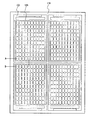
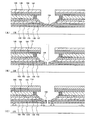
次に、このような表示装置100の詳細を、製造工程を参照しながら説明する。図2は、画素領域108などが設けられる第1の基板102が複数個配置された態様を示す平面図である。図2は、大面積のマザーガラス基板から複数の表示パネルを多面取りする一例を示している。また、図2で示すA−B切断線に沿った断面構造を図3及び図4に示す。図3及び図4は本実施形態で示す表示装置の製造工程を説明する図である。
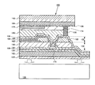
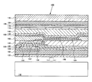
図6及び図7を参照して、本実施形態における表示装置の詳細を説明する。図6は、表示装置100における周縁部の構成を示し、図7は画素106における有機EL素子146と、これに接続するトランジスタ144の構成を示す。以下の説明では、図6及び図7の両図面を参照する。
本発明の一実施形態に係る表示装置の構成を図8に示す。図8で示す表示装置の構成は、第2の基板104が異なる以外は、第1の実施形態と同様であるため、差違のある部分について説明する。
本発明の一実施形態に係る表示装置の構成を図9に示す。図9に示す表示装置の構成は、第1の基板102の構成が異なる以外は、第1の実施形態又は第2の実施形態と同様の構成が適用できるため、差違のある部分について説明する。
Claims (11)
- 表示素子を含む画素が複数個配列した画素領域が設けられた樹脂材料でなる第1の基板と、
前記第1の基板と対向して配置され、前記画素領域を内設するように設けられた第2の基板と、を備え、
前記第1の基板の外周側面が傾斜面であり、前記第1の基板の上層、下層及び前記外周側面を覆うバリア層を有することを特徴とする表示装置。 - 前記バリア層は、前記第1の基板の下層に設けられた第1のバリア層と、前記第1の基板の上層に設けられた第2のバリア層とを有し、
前記第2のバリア層は、前記外周側面に沿って設けられ、前記第1の基板の外側領域で前記第1のバリア層と接していることを特徴とする請求項1に記載の表示装置。 - 前記バリア層が、無機材料であることを特徴とする請求項1に記載の表示装置。
- 前記無機材料が、窒化シリコン、酸化シリコン、酸窒化シリコン及び酸化アルミニウムのうち少なくとも一種であることを特徴とする請求項3に記載の表示装置。
- 前記第1の基板と前記第2のバリア層との間に、金属材料でなる第3のバリア層がさらに設けられていることを特徴とする請求項1に記載の表示装置。
- 前記第3のバリア層の外側領域で、前記第1のバリア層と前記第2のバリア層が接していることを特徴とする請求項5に記載の表示装置。
- 前記金属材料がチタン(Ti)であることを特徴とする請求項5に記載の表示装置。
- 前記第2の基板は樹脂材料で形成され、前記第2の基板の外周側面が傾斜面であり、前記外周側面及び前記第1の基板と対向する面に、第4のバリア層を有することを特徴とする請求項1に記載の表示装置。
- 前記画素領域は、トランジスタを形成する複数の層を含み、
前記トランジスタのチャネルを形成する半導体層とゲート電極との間のゲート絶縁層、および前記トランジスタの前記ゲート電極とソース又はドレイン電極との間の層間絶縁層との一方又は双方が、前記第1の基板の外周側面まで延長して設けられ、前記外周側面において前記バリア層と積層されていることを特徴とする請求項1に記載の表示装置。 - 前記画素領域を被覆するパッシベーション層を含み、
前記パッシベーション層が、前記第1の基板の外周側面まで延長して設けられ、前記外周側面において前記パッシベーション層が前記バリア層と積層されていることを特徴とする請求項1に記載の表示装置。 - 前記表示素子が、有機エレクトロルミネセンス素子又は液晶素子であることを特徴とする請求項1に記載の表示装置。
Priority Applications (4)
| Application Number | Priority Date | Filing Date | Title |
|---|---|---|---|
| JP2014071652A JP2015195104A (ja) | 2014-03-31 | 2014-03-31 | 表示装置 |
| KR1020150033699A KR101676948B1 (ko) | 2014-03-31 | 2015-03-11 | 표시 장치 |
| US14/665,881 US9537013B2 (en) | 2014-03-31 | 2015-03-23 | Display device including tapered substrate |
| US15/355,121 US9685631B2 (en) | 2014-03-31 | 2016-11-18 | Display device including tapered substrate |
Applications Claiming Priority (1)
| Application Number | Priority Date | Filing Date | Title |
|---|---|---|---|
| JP2014071652A JP2015195104A (ja) | 2014-03-31 | 2014-03-31 | 表示装置 |
Publications (2)
| Publication Number | Publication Date |
|---|---|
| JP2015195104A true JP2015195104A (ja) | 2015-11-05 |
| JP2015195104A5 JP2015195104A5 (ja) | 2017-04-27 |
Family
ID=54191598
Family Applications (1)
| Application Number | Title | Priority Date | Filing Date |
|---|---|---|---|
| JP2014071652A Withdrawn JP2015195104A (ja) | 2014-03-31 | 2014-03-31 | 表示装置 |
Country Status (3)
| Country | Link |
|---|---|
| US (2) | US9537013B2 (ja) |
| JP (1) | JP2015195104A (ja) |
| KR (1) | KR101676948B1 (ja) |
Cited By (3)
| Publication number | Priority date | Publication date | Assignee | Title |
|---|---|---|---|---|
| JPWO2017094086A1 (ja) * | 2015-11-30 | 2018-09-13 | パイオニア株式会社 | 発光装置 |
| WO2018235206A1 (ja) * | 2017-06-21 | 2018-12-27 | シャープ株式会社 | 表示デバイス、表示デバイスの製造方法、表示デバイスの製造装置 |
| WO2019171555A1 (ja) * | 2018-03-08 | 2019-09-12 | シャープ株式会社 | 可撓性表示装置の製造方法、および非可撓性基板 |
Families Citing this family (20)
| Publication number | Priority date | Publication date | Assignee | Title |
|---|---|---|---|---|
| US9947894B2 (en) * | 2014-05-16 | 2018-04-17 | Sharp Kabushiki Kaisha | Sealing film, organic el element, and organic el display device |
| JP2016091841A (ja) * | 2014-11-06 | 2016-05-23 | 株式会社Joled | 有機発光デバイスと有機表示装置 |
| JP6890372B2 (ja) * | 2015-06-08 | 2021-06-18 | アルプスアルパイン株式会社 | 車載入力装置 |
| JP6684564B2 (ja) * | 2015-10-14 | 2020-04-22 | 株式会社ジャパンディスプレイ | 有機el表示装置 |
| KR102402606B1 (ko) * | 2015-10-19 | 2022-05-27 | 삼성디스플레이 주식회사 | 플렉서블 디스플레이 장치 및 그 제조방법 |
| KR102552272B1 (ko) * | 2015-11-20 | 2023-07-07 | 삼성디스플레이 주식회사 | 유기 발광 표시 장치 및 그 제조 방법 |
| KR102340066B1 (ko) | 2016-04-07 | 2021-12-15 | 가부시키가이샤 한도오따이 에네루기 켄큐쇼 | 박리 방법 및 플렉시블 디바이스의 제작 방법 |
| KR102694860B1 (ko) * | 2016-09-23 | 2024-08-13 | 삼성디스플레이 주식회사 | 표시 장치 및 그 제조 방법 |
| CN108062176B (zh) * | 2016-11-09 | 2021-07-09 | 东友精细化工有限公司 | 触摸传感器层叠体及其制造方法 |
| KR102326221B1 (ko) | 2017-07-31 | 2021-11-12 | 엘지디스플레이 주식회사 | 디스플레이 장치 및 그 제조 방법 |
| KR102489711B1 (ko) | 2017-10-12 | 2023-01-19 | 삼성디스플레이 주식회사 | 표시 장치 |
| JP7032173B2 (ja) | 2018-02-27 | 2022-03-08 | 株式会社ジャパンディスプレイ | 表示装置 |
| CN110311061B (zh) * | 2019-08-14 | 2021-10-15 | 京东方科技集团股份有限公司 | 显示装置、显示面板及其制备方法 |
| CN111799296A (zh) * | 2019-08-16 | 2020-10-20 | 合肥维信诺科技有限公司 | 一种显示面板的制备方法、显示面板及显示装置 |
| CN110808270A (zh) * | 2019-11-12 | 2020-02-18 | 杭州追猎科技有限公司 | 一种有机发光面板封装结构 |
| CN110808339A (zh) * | 2019-11-13 | 2020-02-18 | 杭州追猎科技有限公司 | 一种有机发光面板 |
| EP4340579A3 (en) * | 2020-03-23 | 2024-06-12 | BOE Technology Group Co., Ltd. | Display substrate, preparation method thereof, display mother plate and display device |
| KR102747402B1 (ko) * | 2020-04-03 | 2024-12-30 | 삼성디스플레이 주식회사 | 표시 패널 및 이를 포함하는 표시 장치 |
| CN111554831B (zh) * | 2020-06-15 | 2023-01-13 | 京东方科技集团股份有限公司 | 柔性显示基板及其制备方法、显示装置 |
| CN113346031B (zh) * | 2021-05-28 | 2023-05-23 | 京东方科技集团股份有限公司 | 显示装置 |
Citations (8)
| Publication number | Priority date | Publication date | Assignee | Title |
|---|---|---|---|---|
| JP2003086356A (ja) * | 2001-09-06 | 2003-03-20 | Semiconductor Energy Lab Co Ltd | 発光装置及び電子機器 |
| JP2003115388A (ja) * | 2001-10-01 | 2003-04-18 | Semiconductor Energy Lab Co Ltd | 発光装置及び電子機器、及び有機偏光フィルム |
| JP2004299230A (ja) * | 2003-03-31 | 2004-10-28 | Dainippon Printing Co Ltd | ガスバリア性基板 |
| JP2011227369A (ja) * | 2010-04-22 | 2011-11-10 | Hitachi Displays Ltd | 画像表示装置及びその製造方法 |
| US20110291544A1 (en) * | 2010-05-31 | 2011-12-01 | Industrial Technology Research Institute | Gas barrier substrate, package of organic electro-luminenscent device and packaging method thereof |
| JP2013165007A (ja) * | 2012-02-13 | 2013-08-22 | Panasonic Corp | 有機エレクトロルミネッセンス素子及びその製造方法 |
| WO2013133256A1 (ja) * | 2012-03-06 | 2013-09-12 | リンテック株式会社 | ガスバリアフィルム積層体、粘着フィルム、および電子部材 |
| JP2013186984A (ja) * | 2012-03-07 | 2013-09-19 | Panasonic Corp | 複合基板構造及びその作製方法、並びに、有機エレクトロルミネッセンス素子 |
Family Cites Families (2)
| Publication number | Priority date | Publication date | Assignee | Title |
|---|---|---|---|---|
| AU2003288999A1 (en) | 2002-12-19 | 2004-07-14 | Semiconductor Energy Laboratory Co., Ltd. | Display unit and method of fabricating display unit |
| JP4508219B2 (ja) * | 2007-07-19 | 2010-07-21 | コニカミノルタホールディングス株式会社 | 有機エレクトロルミネッセンス表示装置及び有機エレクトロルミネッセンス表示素子の封止方法 |
-
2014
- 2014-03-31 JP JP2014071652A patent/JP2015195104A/ja not_active Withdrawn
-
2015
- 2015-03-11 KR KR1020150033699A patent/KR101676948B1/ko active IP Right Grant
- 2015-03-23 US US14/665,881 patent/US9537013B2/en active Active
-
2016
- 2016-11-18 US US15/355,121 patent/US9685631B2/en not_active Expired - Fee Related
Patent Citations (8)
| Publication number | Priority date | Publication date | Assignee | Title |
|---|---|---|---|---|
| JP2003086356A (ja) * | 2001-09-06 | 2003-03-20 | Semiconductor Energy Lab Co Ltd | 発光装置及び電子機器 |
| JP2003115388A (ja) * | 2001-10-01 | 2003-04-18 | Semiconductor Energy Lab Co Ltd | 発光装置及び電子機器、及び有機偏光フィルム |
| JP2004299230A (ja) * | 2003-03-31 | 2004-10-28 | Dainippon Printing Co Ltd | ガスバリア性基板 |
| JP2011227369A (ja) * | 2010-04-22 | 2011-11-10 | Hitachi Displays Ltd | 画像表示装置及びその製造方法 |
| US20110291544A1 (en) * | 2010-05-31 | 2011-12-01 | Industrial Technology Research Institute | Gas barrier substrate, package of organic electro-luminenscent device and packaging method thereof |
| JP2013165007A (ja) * | 2012-02-13 | 2013-08-22 | Panasonic Corp | 有機エレクトロルミネッセンス素子及びその製造方法 |
| WO2013133256A1 (ja) * | 2012-03-06 | 2013-09-12 | リンテック株式会社 | ガスバリアフィルム積層体、粘着フィルム、および電子部材 |
| JP2013186984A (ja) * | 2012-03-07 | 2013-09-19 | Panasonic Corp | 複合基板構造及びその作製方法、並びに、有機エレクトロルミネッセンス素子 |
Cited By (4)
| Publication number | Priority date | Publication date | Assignee | Title |
|---|---|---|---|---|
| JPWO2017094086A1 (ja) * | 2015-11-30 | 2018-09-13 | パイオニア株式会社 | 発光装置 |
| WO2018235206A1 (ja) * | 2017-06-21 | 2018-12-27 | シャープ株式会社 | 表示デバイス、表示デバイスの製造方法、表示デバイスの製造装置 |
| US10991906B2 (en) | 2017-06-21 | 2021-04-27 | Sharp Kabushiki Kaisha | Display device, method for manufacturing display device, and manufacturing apparatus of display device |
| WO2019171555A1 (ja) * | 2018-03-08 | 2019-09-12 | シャープ株式会社 | 可撓性表示装置の製造方法、および非可撓性基板 |
Also Published As
| Publication number | Publication date |
|---|---|
| US20170069874A1 (en) | 2017-03-09 |
| KR101676948B1 (ko) | 2016-11-29 |
| US9685631B2 (en) | 2017-06-20 |
| US9537013B2 (en) | 2017-01-03 |
| KR20150113835A (ko) | 2015-10-08 |
| US20150280172A1 (en) | 2015-10-01 |
Similar Documents
| Publication | Publication Date | Title |
|---|---|---|
| JP2015195104A (ja) | 表示装置 | |
| US9153631B2 (en) | Organic light emitting diode display device | |
| US11069876B2 (en) | Organic electroluminescence display device and manufacturing method thereof | |
| US10347862B2 (en) | EL display device and method for manufacturing EL display device | |
| TWI747461B (zh) | 具有基板孔的顯示裝置 | |
| KR101421168B1 (ko) | 유기전계발광 표시소자 및 그 제조방법 | |
| JP2010257957A (ja) | 有機エレクトロルミネッセンス装置 | |
| KR20180045942A (ko) | 관통홀을 통해 기판의 앞면과 배면을 연결한 평판 표시장치 | |
| WO2016199739A1 (ja) | El表示装置及びel表示装置の製造方法 | |
| JPWO2015029608A1 (ja) | エレクトロルミネッセンス装置、及びその製造方法 | |
| KR20190030951A (ko) | 표시 장치 | |
| JP2018181578A (ja) | 表示装置 | |
| US20150171150A1 (en) | Manufacturing method of organic light emitting diode display device | |
| US10170713B2 (en) | Display device and manufacturing method therefor | |
| US9692011B2 (en) | Electroluminescent apparatus | |
| KR20150136798A (ko) | 유기 발광 표시 패널 및 그의 제조 방법 | |
| TWI609603B (zh) | Display device and its manufacturing method | |
| KR102542133B1 (ko) | 부식이 방지된 표시소자 | |
| KR102449048B1 (ko) | 유기 발광 표시 장치 | |
| KR102200258B1 (ko) | 플렉서블 디스플레이 장치 및 그의 제조 방법 | |
| JP2017174641A (ja) | 表示装置の製造方法 | |
| WO2014123067A1 (ja) | エレクトロルミネッセンス装置 | |
| JP6717700B2 (ja) | 表示装置の製造方法 | |
| JP2009181865A (ja) | 表示装置 | |
| KR20180074165A (ko) | 유기 발광 표시 장치 및 그의 제조 방법 |
Legal Events
| Date | Code | Title | Description |
|---|---|---|---|
| A521 | Request for written amendment filed |
Free format text: JAPANESE INTERMEDIATE CODE: A523 Effective date: 20170321 |
|
| A621 | Written request for application examination |
Free format text: JAPANESE INTERMEDIATE CODE: A621 Effective date: 20170321 |
|
| A977 | Report on retrieval |
Free format text: JAPANESE INTERMEDIATE CODE: A971007 Effective date: 20180216 |
|
| A131 | Notification of reasons for refusal |
Free format text: JAPANESE INTERMEDIATE CODE: A131 Effective date: 20180227 |
|
| A521 | Request for written amendment filed |
Free format text: JAPANESE INTERMEDIATE CODE: A523 Effective date: 20180424 |
|
| A131 | Notification of reasons for refusal |
Free format text: JAPANESE INTERMEDIATE CODE: A131 Effective date: 20181002 |
|
| A761 | Written withdrawal of application |
Free format text: JAPANESE INTERMEDIATE CODE: A761 Effective date: 20181206 |