JP2015109369A - 縦型半導体装置 - Google Patents
縦型半導体装置 Download PDFInfo
- Publication number
- JP2015109369A JP2015109369A JP2013251994A JP2013251994A JP2015109369A JP 2015109369 A JP2015109369 A JP 2015109369A JP 2013251994 A JP2013251994 A JP 2013251994A JP 2013251994 A JP2013251994 A JP 2013251994A JP 2015109369 A JP2015109369 A JP 2015109369A
- Authority
- JP
- Japan
- Prior art keywords
- layer
- buffer
- buffer region
- semiconductor layer
- region
- Prior art date
- Legal status (The legal status is an assumption and is not a legal conclusion. Google has not performed a legal analysis and makes no representation as to the accuracy of the status listed.)
- Granted
Links
Images






Classifications
-
- H—ELECTRICITY
- H10—SEMICONDUCTOR DEVICES; ELECTRIC SOLID-STATE DEVICES NOT OTHERWISE PROVIDED FOR
- H10D—INORGANIC ELECTRIC SEMICONDUCTOR DEVICES
- H10D12/00—Bipolar devices controlled by the field effect, e.g. insulated-gate bipolar transistors [IGBT]
- H10D12/411—Insulated-gate bipolar transistors [IGBT]
- H10D12/441—Vertical IGBTs
- H10D12/461—Vertical IGBTs having non-planar surfaces, e.g. having trenches, recesses or pillars in the surfaces of the emitter, base or collector regions
- H10D12/481—Vertical IGBTs having non-planar surfaces, e.g. having trenches, recesses or pillars in the surfaces of the emitter, base or collector regions having gate structures on slanted surfaces, on vertical surfaces, or in grooves, e.g. trench gate IGBTs
-
- H—ELECTRICITY
- H10—SEMICONDUCTOR DEVICES; ELECTRIC SOLID-STATE DEVICES NOT OTHERWISE PROVIDED FOR
- H10D—INORGANIC ELECTRIC SEMICONDUCTOR DEVICES
- H10D12/00—Bipolar devices controlled by the field effect, e.g. insulated-gate bipolar transistors [IGBT]
-
- H—ELECTRICITY
- H10—SEMICONDUCTOR DEVICES; ELECTRIC SOLID-STATE DEVICES NOT OTHERWISE PROVIDED FOR
- H10D—INORGANIC ELECTRIC SEMICONDUCTOR DEVICES
- H10D30/00—Field-effect transistors [FET]
- H10D30/60—Insulated-gate field-effect transistors [IGFET]
-
- H—ELECTRICITY
- H10—SEMICONDUCTOR DEVICES; ELECTRIC SOLID-STATE DEVICES NOT OTHERWISE PROVIDED FOR
- H10D—INORGANIC ELECTRIC SEMICONDUCTOR DEVICES
- H10D30/00—Field-effect transistors [FET]
- H10D30/60—Insulated-gate field-effect transistors [IGFET]
- H10D30/64—Double-diffused metal-oxide semiconductor [DMOS] FETs
- H10D30/66—Vertical DMOS [VDMOS] FETs
-
- H—ELECTRICITY
- H10—SEMICONDUCTOR DEVICES; ELECTRIC SOLID-STATE DEVICES NOT OTHERWISE PROVIDED FOR
- H10D—INORGANIC ELECTRIC SEMICONDUCTOR DEVICES
- H10D62/00—Semiconductor bodies, or regions thereof, of devices having potential barriers
- H10D62/10—Shapes, relative sizes or dispositions of the regions of the semiconductor bodies; Shapes of the semiconductor bodies
- H10D62/128—Anode regions of diodes
-
- H—ELECTRICITY
- H10—SEMICONDUCTOR DEVICES; ELECTRIC SOLID-STATE DEVICES NOT OTHERWISE PROVIDED FOR
- H10D—INORGANIC ELECTRIC SEMICONDUCTOR DEVICES
- H10D62/00—Semiconductor bodies, or regions thereof, of devices having potential barriers
- H10D62/10—Shapes, relative sizes or dispositions of the regions of the semiconductor bodies; Shapes of the semiconductor bodies
- H10D62/129—Cathode regions of diodes
-
- H—ELECTRICITY
- H10—SEMICONDUCTOR DEVICES; ELECTRIC SOLID-STATE DEVICES NOT OTHERWISE PROVIDED FOR
- H10D—INORGANIC ELECTRIC SEMICONDUCTOR DEVICES
- H10D62/00—Semiconductor bodies, or regions thereof, of devices having potential barriers
- H10D62/10—Shapes, relative sizes or dispositions of the regions of the semiconductor bodies; Shapes of the semiconductor bodies
- H10D62/13—Semiconductor regions connected to electrodes carrying current to be rectified, amplified or switched, e.g. source or drain regions
- H10D62/141—Anode or cathode regions of thyristors; Collector or emitter regions of gated bipolar-mode devices, e.g. of IGBTs
-
- H—ELECTRICITY
- H10—SEMICONDUCTOR DEVICES; ELECTRIC SOLID-STATE DEVICES NOT OTHERWISE PROVIDED FOR
- H10D—INORGANIC ELECTRIC SEMICONDUCTOR DEVICES
- H10D62/00—Semiconductor bodies, or regions thereof, of devices having potential barriers
- H10D62/10—Shapes, relative sizes or dispositions of the regions of the semiconductor bodies; Shapes of the semiconductor bodies
- H10D62/13—Semiconductor regions connected to electrodes carrying current to be rectified, amplified or switched, e.g. source or drain regions
- H10D62/141—Anode or cathode regions of thyristors; Collector or emitter regions of gated bipolar-mode devices, e.g. of IGBTs
- H10D62/142—Anode regions of thyristors or collector regions of gated bipolar-mode devices
-
- H—ELECTRICITY
- H10—SEMICONDUCTOR DEVICES; ELECTRIC SOLID-STATE DEVICES NOT OTHERWISE PROVIDED FOR
- H10D—INORGANIC ELECTRIC SEMICONDUCTOR DEVICES
- H10D62/00—Semiconductor bodies, or regions thereof, of devices having potential barriers
- H10D62/10—Shapes, relative sizes or dispositions of the regions of the semiconductor bodies; Shapes of the semiconductor bodies
- H10D62/13—Semiconductor regions connected to electrodes carrying current to be rectified, amplified or switched, e.g. source or drain regions
- H10D62/149—Source or drain regions of field-effect devices
- H10D62/151—Source or drain regions of field-effect devices of IGFETs
- H10D62/156—Drain regions of DMOS transistors
- H10D62/157—Impurity concentrations or distributions
-
- H—ELECTRICITY
- H10—SEMICONDUCTOR DEVICES; ELECTRIC SOLID-STATE DEVICES NOT OTHERWISE PROVIDED FOR
- H10D—INORGANIC ELECTRIC SEMICONDUCTOR DEVICES
- H10D62/00—Semiconductor bodies, or regions thereof, of devices having potential barriers
- H10D62/60—Impurity distributions or concentrations
-
- H—ELECTRICITY
- H10—SEMICONDUCTOR DEVICES; ELECTRIC SOLID-STATE DEVICES NOT OTHERWISE PROVIDED FOR
- H10D—INORGANIC ELECTRIC SEMICONDUCTOR DEVICES
- H10D64/00—Electrodes of devices having potential barriers
- H10D64/20—Electrodes characterised by their shapes, relative sizes or dispositions
-
- H—ELECTRICITY
- H10—SEMICONDUCTOR DEVICES; ELECTRIC SOLID-STATE DEVICES NOT OTHERWISE PROVIDED FOR
- H10D—INORGANIC ELECTRIC SEMICONDUCTOR DEVICES
- H10D64/00—Electrodes of devices having potential barriers
- H10D64/20—Electrodes characterised by their shapes, relative sizes or dispositions
- H10D64/23—Electrodes carrying the current to be rectified, amplified, oscillated or switched, e.g. sources, drains, anodes or cathodes
-
- H—ELECTRICITY
- H10—SEMICONDUCTOR DEVICES; ELECTRIC SOLID-STATE DEVICES NOT OTHERWISE PROVIDED FOR
- H10D—INORGANIC ELECTRIC SEMICONDUCTOR DEVICES
- H10D8/00—Diodes
-
- H—ELECTRICITY
- H10—SEMICONDUCTOR DEVICES; ELECTRIC SOLID-STATE DEVICES NOT OTHERWISE PROVIDED FOR
- H10D—INORGANIC ELECTRIC SEMICONDUCTOR DEVICES
- H10D8/00—Diodes
- H10D8/411—PN diodes having planar bodies
Landscapes
- Electrodes Of Semiconductors (AREA)
- Metal-Oxide And Bipolar Metal-Oxide Semiconductor Integrated Circuits (AREA)
Abstract
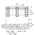
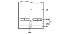
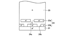
【解決手段】 バッファ層23は、n+型の第1バッファ領域23aとn+型の第2バッファ領域23bを有する。第1バッファ領域23aは、半導体層20の第1主面20aから第1深さD1に形成されており、その不純物濃度がドリフト層25の不純物濃度よりも濃い。第2バッファ領域23bは、半導体層20の第1主面20aから第1深さD1よりも浅い第2深さD2に形成されており、その不純物濃度がドリフト層25の不純物濃度よりも濃い。第1バッファ領域23aは、半導体層20の第1深さD1の面内に開口24aを画定している。第2バッファ領域23bは、半導体層20の第2深さD2の面内に開口24bを画定している。
【選択図】図1
Description
(1)図1に示されるように、半導体装置1では、半導体層20の厚み方向に観測したときに、第1バッファ領域23aで画定される開口24aの範囲と第2バッファ領域23bで画定される開口24bの範囲が重複していない。このため、半導体装置1がターンオフしたときに、ドリフト層25とベース層27の接合面から伸びる空乏層がコレクタ層21に達することが確実に防止される。これにより、ベース層27とコレクタ層21の間のパンチスルーの発生が防止され、リーク電流の増大が抑制される。
Claims (2)
- 縦型半導体装置であって、
半導体層と、
前記半導体層の第1主面を被膜する第1主電極と、
前記半導体層の第2主面を被膜する第2主電極と、を備えており、
前記半導体層は、
バッファ層と、
前記バッファ層に接しており、前記バッファ層よりも前記第2主面側に配置されている第1導電型の第1半導体層と、
前記第1半導体層に接しており、前記第1半導体層よりも前記第2主面側に配置されている第2導電型の第2半導体層と、を有しており、
前記バッファ層は、
前記第1主面から第1深さに形成されており、その不純物濃度が前記第1半導体層の不純物濃度よりも濃い第1導電型の第1バッファ領域と
前記第1主面から前記第1深さよりも浅い第2深さに形成されており、その不純物濃度が前記第1半導体層の不純物濃度よりも濃い第1導電型の第2バッファ領域と、を有しており、
前記第1バッファ領域は、前記半導体層の前記第1深さの面内に開口を画定しており、
前記第2バッファ領域は、前記半導体層の前記第2深さの面内に開口を画定している縦型半導体装置。 - 前記半導体層の深さ方向に沿って観測したときに、前記第1バッファ領域で画定される開口の位置と前記第2バッファ領域で画定される開口の位置が一致しない請求項1に記載の半導体装置。
Priority Applications (5)
| Application Number | Priority Date | Filing Date | Title |
|---|---|---|---|
| JP2013251994A JP6092760B2 (ja) | 2013-12-05 | 2013-12-05 | 縦型半導体装置 |
| US15/028,868 US20160276469A1 (en) | 2013-12-05 | 2014-10-07 | Vertical-type semiconductor device |
| DE112014005534.4T DE112014005534T5 (de) | 2013-12-05 | 2014-10-07 | Halbleitereinrichtung des vertikalen Typs |
| PCT/JP2014/076781 WO2015083434A1 (ja) | 2013-12-05 | 2014-10-07 | 縦型半導体装置 |
| CN201480066442.4A CN105793990A (zh) | 2013-12-05 | 2014-10-07 | 纵型半导体装置 |
Applications Claiming Priority (1)
| Application Number | Priority Date | Filing Date | Title |
|---|---|---|---|
| JP2013251994A JP6092760B2 (ja) | 2013-12-05 | 2013-12-05 | 縦型半導体装置 |
Publications (2)
| Publication Number | Publication Date |
|---|---|
| JP2015109369A true JP2015109369A (ja) | 2015-06-11 |
| JP6092760B2 JP6092760B2 (ja) | 2017-03-08 |
Family
ID=53273211
Family Applications (1)
| Application Number | Title | Priority Date | Filing Date |
|---|---|---|---|
| JP2013251994A Active JP6092760B2 (ja) | 2013-12-05 | 2013-12-05 | 縦型半導体装置 |
Country Status (5)
| Country | Link |
|---|---|
| US (1) | US20160276469A1 (ja) |
| JP (1) | JP6092760B2 (ja) |
| CN (1) | CN105793990A (ja) |
| DE (1) | DE112014005534T5 (ja) |
| WO (1) | WO2015083434A1 (ja) |
Families Citing this family (5)
| Publication number | Priority date | Publication date | Assignee | Title |
|---|---|---|---|---|
| JP6185511B2 (ja) * | 2015-05-26 | 2017-08-23 | トヨタ自動車株式会社 | 半導体装置 |
| JP2017188569A (ja) * | 2016-04-06 | 2017-10-12 | 三菱電機株式会社 | 半導体装置およびその製造方法 |
| JP7246983B2 (ja) | 2019-03-20 | 2023-03-28 | 株式会社東芝 | 半導体装置 |
| JP7528628B2 (ja) * | 2020-08-20 | 2024-08-06 | 三菱電機株式会社 | 半導体装置および半導体装置の製造方法 |
| JP7717010B2 (ja) * | 2022-03-08 | 2025-08-01 | 株式会社デンソー | 半導体装置 |
Citations (5)
| Publication number | Priority date | Publication date | Assignee | Title |
|---|---|---|---|---|
| JPH0637335A (ja) * | 1992-07-15 | 1994-02-10 | Naoshige Tamamushi | 埋込み構造もしくは切込み構造を有する静電誘導ダイオード |
| JPH09162398A (ja) * | 1995-12-11 | 1997-06-20 | Mitsubishi Electric Corp | 半導体装置およびその製造方法 |
| JP2002100772A (ja) * | 2000-07-17 | 2002-04-05 | Toshiba Corp | 電力用半導体装置及びその製造方法 |
| JP2012059734A (ja) * | 2010-09-03 | 2012-03-22 | Panasonic Corp | 半導体装置及びその製造方法 |
| JP2013065735A (ja) * | 2011-09-19 | 2013-04-11 | Denso Corp | 半導体装置 |
Family Cites Families (7)
| Publication number | Priority date | Publication date | Assignee | Title |
|---|---|---|---|---|
| DE19843659A1 (de) * | 1998-09-23 | 2000-04-06 | Siemens Ag | Halbleiterbauelement mit strukturiertem Halbleiterkörper |
| JP4655350B2 (ja) * | 2000-10-31 | 2011-03-23 | 富士電機システムズ株式会社 | 半導体装置 |
| DE10361136B4 (de) * | 2003-12-23 | 2005-10-27 | Infineon Technologies Ag | Halbleiterdiode und IGBT |
| US7687891B2 (en) * | 2007-05-14 | 2010-03-30 | Infineon Technologies Ag | Diode having one or more zones of a first conductivity type and one or more zones of a second conductivity type each located within a layer of the second conductivity type |
| US8466491B2 (en) * | 2011-05-12 | 2013-06-18 | Infineon Technologies Austria Ag | Semiconductor component with improved softness |
| CN102683404A (zh) * | 2012-05-22 | 2012-09-19 | 上海宏力半导体制造有限公司 | 绝缘栅双极型晶体管及其制造方法 |
| CN202917494U (zh) * | 2012-11-29 | 2013-05-01 | 杭州士兰集成电路有限公司 | 场截止缓冲层及具有场截止缓冲层的igbt器件 |
-
2013
- 2013-12-05 JP JP2013251994A patent/JP6092760B2/ja active Active
-
2014
- 2014-10-07 DE DE112014005534.4T patent/DE112014005534T5/de not_active Withdrawn
- 2014-10-07 US US15/028,868 patent/US20160276469A1/en not_active Abandoned
- 2014-10-07 WO PCT/JP2014/076781 patent/WO2015083434A1/ja not_active Ceased
- 2014-10-07 CN CN201480066442.4A patent/CN105793990A/zh active Pending
Patent Citations (5)
| Publication number | Priority date | Publication date | Assignee | Title |
|---|---|---|---|---|
| JPH0637335A (ja) * | 1992-07-15 | 1994-02-10 | Naoshige Tamamushi | 埋込み構造もしくは切込み構造を有する静電誘導ダイオード |
| JPH09162398A (ja) * | 1995-12-11 | 1997-06-20 | Mitsubishi Electric Corp | 半導体装置およびその製造方法 |
| JP2002100772A (ja) * | 2000-07-17 | 2002-04-05 | Toshiba Corp | 電力用半導体装置及びその製造方法 |
| JP2012059734A (ja) * | 2010-09-03 | 2012-03-22 | Panasonic Corp | 半導体装置及びその製造方法 |
| JP2013065735A (ja) * | 2011-09-19 | 2013-04-11 | Denso Corp | 半導体装置 |
Also Published As
| Publication number | Publication date |
|---|---|
| JP6092760B2 (ja) | 2017-03-08 |
| US20160276469A1 (en) | 2016-09-22 |
| WO2015083434A1 (ja) | 2015-06-11 |
| DE112014005534T5 (de) | 2016-08-25 |
| CN105793990A (zh) | 2016-07-20 |
Similar Documents
| Publication | Publication Date | Title |
|---|---|---|
| JP7673846B2 (ja) | 半導体装置 | |
| JP7632545B2 (ja) | 半導体装置 | |
| JP5787853B2 (ja) | 電力用半導体装置 | |
| US9059238B2 (en) | Semiconductor device | |
| US9147758B2 (en) | Semiconductor device | |
| US9853024B2 (en) | Semiconductor device | |
| JP6451869B2 (ja) | 半導体装置 | |
| US9214535B2 (en) | Semiconductor device | |
| WO2017155122A1 (ja) | 半導体装置 | |
| US9312372B2 (en) | Semiconductor device | |
| JP6958093B2 (ja) | 半導体装置 | |
| JP5865618B2 (ja) | 半導体装置 | |
| JP7414047B2 (ja) | 半導体装置 | |
| JP6139312B2 (ja) | 半導体装置 | |
| JP6416056B2 (ja) | 半導体装置 | |
| WO2018220879A1 (ja) | 半導体装置 | |
| WO2017038389A1 (ja) | 半導体装置 | |
| JP5480084B2 (ja) | 半導体装置 | |
| JP2013197122A (ja) | 半導体装置 | |
| JP2016040820A (ja) | 半導体装置 | |
| JP5865860B2 (ja) | 半導体装置 | |
| US12199092B2 (en) | Semiconductor apparatus | |
| JP7114901B2 (ja) | 半導体装置 | |
| JP6092760B2 (ja) | 縦型半導体装置 | |
| JP6173987B2 (ja) | 半導体装置 |
Legal Events
| Date | Code | Title | Description |
|---|---|---|---|
| A621 | Written request for application examination |
Free format text: JAPANESE INTERMEDIATE CODE: A621 Effective date: 20160121 |
|
| A131 | Notification of reasons for refusal |
Free format text: JAPANESE INTERMEDIATE CODE: A131 Effective date: 20160913 |
|
| A521 | Request for written amendment filed |
Free format text: JAPANESE INTERMEDIATE CODE: A523 Effective date: 20161018 |
|
| TRDD | Decision of grant or rejection written | ||
| A01 | Written decision to grant a patent or to grant a registration (utility model) |
Free format text: JAPANESE INTERMEDIATE CODE: A01 Effective date: 20170207 |
|
| A61 | First payment of annual fees (during grant procedure) |
Free format text: JAPANESE INTERMEDIATE CODE: A61 Effective date: 20170209 |
|
| R150 | Certificate of patent or registration of utility model |
Ref document number: 6092760 Country of ref document: JP Free format text: JAPANESE INTERMEDIATE CODE: R150 |
|
| R250 | Receipt of annual fees |
Free format text: JAPANESE INTERMEDIATE CODE: R250 |
|
| S111 | Request for change of ownership or part of ownership |
Free format text: JAPANESE INTERMEDIATE CODE: R313117 |
|
| R350 | Written notification of registration of transfer |
Free format text: JAPANESE INTERMEDIATE CODE: R350 |
|
| R250 | Receipt of annual fees |
Free format text: JAPANESE INTERMEDIATE CODE: R250 |
|
| R250 | Receipt of annual fees |
Free format text: JAPANESE INTERMEDIATE CODE: R250 |
|
| R250 | Receipt of annual fees |
Free format text: JAPANESE INTERMEDIATE CODE: R250 |
|
| R250 | Receipt of annual fees |
Free format text: JAPANESE INTERMEDIATE CODE: R250 |
|
| R250 | Receipt of annual fees |
Free format text: JAPANESE INTERMEDIATE CODE: R250 |
|
| R250 | Receipt of annual fees |
Free format text: JAPANESE INTERMEDIATE CODE: R250 |