JP2014192452A - Electronic component built-in substrate and manufacturing method of the same - Google Patents
Electronic component built-in substrate and manufacturing method of the same Download PDFInfo
- Publication number
- JP2014192452A JP2014192452A JP2013068549A JP2013068549A JP2014192452A JP 2014192452 A JP2014192452 A JP 2014192452A JP 2013068549 A JP2013068549 A JP 2013068549A JP 2013068549 A JP2013068549 A JP 2013068549A JP 2014192452 A JP2014192452 A JP 2014192452A
- Authority
- JP
- Japan
- Prior art keywords
- insulating layer
- substrate
- layer
- electronic component
- wiring
- Prior art date
- Legal status (The legal status is an assumption and is not a legal conclusion. Google has not performed a legal analysis and makes no representation as to the accuracy of the status listed.)
- Granted
Links
Images


Classifications
-
- H—ELECTRICITY
- H01—ELECTRIC ELEMENTS
- H01L—SEMICONDUCTOR DEVICES NOT COVERED BY CLASS H10
- H01L23/00—Details of semiconductor or other solid state devices
- H01L23/48—Arrangements for conducting electric current to or from the solid state body in operation, e.g. leads, terminal arrangements ; Selection of materials therefor
- H01L23/488—Arrangements for conducting electric current to or from the solid state body in operation, e.g. leads, terminal arrangements ; Selection of materials therefor consisting of soldered or bonded constructions
- H01L23/498—Leads, i.e. metallisations or lead-frames on insulating substrates, e.g. chip carriers
- H01L23/49866—Leads, i.e. metallisations or lead-frames on insulating substrates, e.g. chip carriers characterised by the materials
- H01L23/49894—Materials of the insulating layers or coatings
-
- H—ELECTRICITY
- H01—ELECTRIC ELEMENTS
- H01L—SEMICONDUCTOR DEVICES NOT COVERED BY CLASS H10
- H01L23/00—Details of semiconductor or other solid state devices
- H01L23/48—Arrangements for conducting electric current to or from the solid state body in operation, e.g. leads, terminal arrangements ; Selection of materials therefor
- H01L23/482—Arrangements for conducting electric current to or from the solid state body in operation, e.g. leads, terminal arrangements ; Selection of materials therefor consisting of lead-in layers inseparably applied to the semiconductor body
- H01L23/485—Arrangements for conducting electric current to or from the solid state body in operation, e.g. leads, terminal arrangements ; Selection of materials therefor consisting of lead-in layers inseparably applied to the semiconductor body consisting of layered constructions comprising conductive layers and insulating layers, e.g. planar contacts
-
- H—ELECTRICITY
- H01—ELECTRIC ELEMENTS
- H01L—SEMICONDUCTOR DEVICES NOT COVERED BY CLASS H10
- H01L23/00—Details of semiconductor or other solid state devices
- H01L23/48—Arrangements for conducting electric current to or from the solid state body in operation, e.g. leads, terminal arrangements ; Selection of materials therefor
- H01L23/488—Arrangements for conducting electric current to or from the solid state body in operation, e.g. leads, terminal arrangements ; Selection of materials therefor consisting of soldered or bonded constructions
- H01L23/498—Leads, i.e. metallisations or lead-frames on insulating substrates, e.g. chip carriers
- H01L23/49822—Multilayer substrates
-
- H—ELECTRICITY
- H05—ELECTRIC TECHNIQUES NOT OTHERWISE PROVIDED FOR
- H05K—PRINTED CIRCUITS; CASINGS OR CONSTRUCTIONAL DETAILS OF ELECTRIC APPARATUS; MANUFACTURE OF ASSEMBLAGES OF ELECTRICAL COMPONENTS
- H05K1/00—Printed circuits
- H05K1/18—Printed circuits structurally associated with non-printed electric components
- H05K1/182—Printed circuits structurally associated with non-printed electric components associated with components mounted in the printed circuit board, e.g. insert mounted components [IMC]
- H05K1/185—Components encapsulated in the insulating substrate of the printed circuit or incorporated in internal layers of a multilayer circuit
-
- H—ELECTRICITY
- H01—ELECTRIC ELEMENTS
- H01L—SEMICONDUCTOR DEVICES NOT COVERED BY CLASS H10
- H01L2224/00—Indexing scheme for arrangements for connecting or disconnecting semiconductor or solid-state bodies and methods related thereto as covered by H01L24/00
- H01L2224/01—Means for bonding being attached to, or being formed on, the surface to be connected, e.g. chip-to-package, die-attach, "first-level" interconnects; Manufacturing methods related thereto
- H01L2224/10—Bump connectors; Manufacturing methods related thereto
- H01L2224/15—Structure, shape, material or disposition of the bump connectors after the connecting process
- H01L2224/16—Structure, shape, material or disposition of the bump connectors after the connecting process of an individual bump connector
- H01L2224/161—Disposition
- H01L2224/16151—Disposition the bump connector connecting between a semiconductor or solid-state body and an item not being a semiconductor or solid-state body, e.g. chip-to-substrate, chip-to-passive
- H01L2224/16221—Disposition the bump connector connecting between a semiconductor or solid-state body and an item not being a semiconductor or solid-state body, e.g. chip-to-substrate, chip-to-passive the body and the item being stacked
- H01L2224/16225—Disposition the bump connector connecting between a semiconductor or solid-state body and an item not being a semiconductor or solid-state body, e.g. chip-to-substrate, chip-to-passive the body and the item being stacked the item being non-metallic, e.g. insulating substrate with or without metallisation
-
- H—ELECTRICITY
- H01—ELECTRIC ELEMENTS
- H01L—SEMICONDUCTOR DEVICES NOT COVERED BY CLASS H10
- H01L2224/00—Indexing scheme for arrangements for connecting or disconnecting semiconductor or solid-state bodies and methods related thereto as covered by H01L24/00
- H01L2224/01—Means for bonding being attached to, or being formed on, the surface to be connected, e.g. chip-to-package, die-attach, "first-level" interconnects; Manufacturing methods related thereto
- H01L2224/26—Layer connectors, e.g. plate connectors, solder or adhesive layers; Manufacturing methods related thereto
- H01L2224/31—Structure, shape, material or disposition of the layer connectors after the connecting process
- H01L2224/32—Structure, shape, material or disposition of the layer connectors after the connecting process of an individual layer connector
- H01L2224/321—Disposition
- H01L2224/32151—Disposition the layer connector connecting between a semiconductor or solid-state body and an item not being a semiconductor or solid-state body, e.g. chip-to-substrate, chip-to-passive
- H01L2224/32221—Disposition the layer connector connecting between a semiconductor or solid-state body and an item not being a semiconductor or solid-state body, e.g. chip-to-substrate, chip-to-passive the body and the item being stacked
- H01L2224/32225—Disposition the layer connector connecting between a semiconductor or solid-state body and an item not being a semiconductor or solid-state body, e.g. chip-to-substrate, chip-to-passive the body and the item being stacked the item being non-metallic, e.g. insulating substrate with or without metallisation
-
- H—ELECTRICITY
- H01—ELECTRIC ELEMENTS
- H01L—SEMICONDUCTOR DEVICES NOT COVERED BY CLASS H10
- H01L2224/00—Indexing scheme for arrangements for connecting or disconnecting semiconductor or solid-state bodies and methods related thereto as covered by H01L24/00
- H01L2224/73—Means for bonding being of different types provided for in two or more of groups H01L2224/10, H01L2224/18, H01L2224/26, H01L2224/34, H01L2224/42, H01L2224/50, H01L2224/63, H01L2224/71
- H01L2224/732—Location after the connecting process
- H01L2224/73201—Location after the connecting process on the same surface
- H01L2224/73203—Bump and layer connectors
- H01L2224/73204—Bump and layer connectors the bump connector being embedded into the layer connector
-
- H—ELECTRICITY
- H01—ELECTRIC ELEMENTS
- H01L—SEMICONDUCTOR DEVICES NOT COVERED BY CLASS H10
- H01L23/00—Details of semiconductor or other solid state devices
- H01L23/12—Mountings, e.g. non-detachable insulating substrates
- H01L23/13—Mountings, e.g. non-detachable insulating substrates characterised by the shape
-
- H—ELECTRICITY
- H01—ELECTRIC ELEMENTS
- H01L—SEMICONDUCTOR DEVICES NOT COVERED BY CLASS H10
- H01L23/00—Details of semiconductor or other solid state devices
- H01L23/52—Arrangements for conducting electric current within the device in operation from one component to another, i.e. interconnections, e.g. wires, lead frames
- H01L23/538—Arrangements for conducting electric current within the device in operation from one component to another, i.e. interconnections, e.g. wires, lead frames the interconnection structure between a plurality of semiconductor chips being formed on, or in, insulating substrates
- H01L23/5389—Arrangements for conducting electric current within the device in operation from one component to another, i.e. interconnections, e.g. wires, lead frames the interconnection structure between a plurality of semiconductor chips being formed on, or in, insulating substrates the chips being integrally enclosed by the interconnect and support structures
-
- H—ELECTRICITY
- H01—ELECTRIC ELEMENTS
- H01L—SEMICONDUCTOR DEVICES NOT COVERED BY CLASS H10
- H01L2924/00—Indexing scheme for arrangements or methods for connecting or disconnecting semiconductor or solid-state bodies as covered by H01L24/00
- H01L2924/15—Details of package parts other than the semiconductor or other solid state devices to be connected
- H01L2924/151—Die mounting substrate
- H01L2924/1517—Multilayer substrate
-
- H—ELECTRICITY
- H01—ELECTRIC ELEMENTS
- H01L—SEMICONDUCTOR DEVICES NOT COVERED BY CLASS H10
- H01L2924/00—Indexing scheme for arrangements or methods for connecting or disconnecting semiconductor or solid-state bodies as covered by H01L24/00
- H01L2924/15—Details of package parts other than the semiconductor or other solid state devices to be connected
- H01L2924/151—Die mounting substrate
- H01L2924/153—Connection portion
- H01L2924/1531—Connection portion the connection portion being formed only on the surface of the substrate opposite to the die mounting surface
- H01L2924/15311—Connection portion the connection portion being formed only on the surface of the substrate opposite to the die mounting surface being a ball array, e.g. BGA
-
- H—ELECTRICITY
- H05—ELECTRIC TECHNIQUES NOT OTHERWISE PROVIDED FOR
- H05K—PRINTED CIRCUITS; CASINGS OR CONSTRUCTIONAL DETAILS OF ELECTRIC APPARATUS; MANUFACTURE OF ASSEMBLAGES OF ELECTRICAL COMPONENTS
- H05K2201/00—Indexing scheme relating to printed circuits covered by H05K1/00
- H05K2201/10—Details of components or other objects attached to or integrated in a printed circuit board
- H05K2201/10613—Details of electrical connections of non-printed components, e.g. special leads
- H05K2201/10621—Components characterised by their electrical contacts
- H05K2201/10636—Leadless chip, e.g. chip capacitor or resistor
-
- H—ELECTRICITY
- H05—ELECTRIC TECHNIQUES NOT OTHERWISE PROVIDED FOR
- H05K—PRINTED CIRCUITS; CASINGS OR CONSTRUCTIONAL DETAILS OF ELECTRIC APPARATUS; MANUFACTURE OF ASSEMBLAGES OF ELECTRICAL COMPONENTS
- H05K2203/00—Indexing scheme relating to apparatus or processes for manufacturing printed circuits covered by H05K3/00
- H05K2203/14—Related to the order of processing steps
- H05K2203/1461—Applying or finishing the circuit pattern after another process, e.g. after filling of vias with conductive paste, after making printed resistors
- H05K2203/1469—Circuit made after mounting or encapsulation of the components
-
- H—ELECTRICITY
- H05—ELECTRIC TECHNIQUES NOT OTHERWISE PROVIDED FOR
- H05K—PRINTED CIRCUITS; CASINGS OR CONSTRUCTIONAL DETAILS OF ELECTRIC APPARATUS; MANUFACTURE OF ASSEMBLAGES OF ELECTRICAL COMPONENTS
- H05K3/00—Apparatus or processes for manufacturing printed circuits
- H05K3/46—Manufacturing multilayer circuits
- H05K3/4602—Manufacturing multilayer circuits characterized by a special circuit board as base or central core whereon additional circuit layers are built or additional circuit boards are laminated
-
- Y—GENERAL TAGGING OF NEW TECHNOLOGICAL DEVELOPMENTS; GENERAL TAGGING OF CROSS-SECTIONAL TECHNOLOGIES SPANNING OVER SEVERAL SECTIONS OF THE IPC; TECHNICAL SUBJECTS COVERED BY FORMER USPC CROSS-REFERENCE ART COLLECTIONS [XRACs] AND DIGESTS
- Y02—TECHNOLOGIES OR APPLICATIONS FOR MITIGATION OR ADAPTATION AGAINST CLIMATE CHANGE
- Y02P—CLIMATE CHANGE MITIGATION TECHNOLOGIES IN THE PRODUCTION OR PROCESSING OF GOODS
- Y02P70/00—Climate change mitigation technologies in the production process for final industrial or consumer products
- Y02P70/50—Manufacturing or production processes characterised by the final manufactured product
Abstract
Description
本発明は電子部品内蔵基板及びその製造方法に関する。 The present invention relates to an electronic component built-in substrate and a method for manufacturing the same.
近年の電子機器の発達に伴い、電子機器に使用される電子部品装置の配線基板は、小型化及び高性能化などが要求されている。これに対応するため、配線基板内に電子部品が内蔵された電子部品内蔵基板が実用化されている。 With the recent development of electronic devices, wiring boards for electronic component devices used in electronic devices are required to be smaller and have higher performance. In order to cope with this, an electronic component built-in board in which an electronic component is built in a wiring board has been put into practical use.
そのような電子部品内蔵基板の一例では、コア基板の開口部に電子部品が配置され、コア基板の両面側にビルドアップ配線が形成される。 In an example of such an electronic component built-in substrate, the electronic component is disposed in the opening of the core substrate, and build-up wiring is formed on both sides of the core substrate.
電子部品内蔵基板を製造する際には、コア基板の開口部に配置された電子部品の周りの隙間に、樹脂フィルムを熱プレスして樹脂を埋め込む工程がある。 When manufacturing an electronic component built-in substrate, there is a process of embedding resin by hot pressing a resin film in a gap around the electronic component arranged in the opening of the core substrate.
特に電子部品の厚みがコア基板の厚みより薄い場合は、埋め込む空間の体積が大きいため、コア基板の開口部で樹脂層が窪んで形成される。樹脂層の平坦性が悪いと、その上に微細な配線層を歩留りよく形成することが困難になる。 In particular, when the thickness of the electronic component is smaller than the thickness of the core substrate, since the volume of the space to be embedded is large, the resin layer is formed to be recessed at the opening of the core substrate. If the flatness of the resin layer is poor, it becomes difficult to form a fine wiring layer on the resin layer with a good yield.
電子部品内蔵基板及びその製造方法において、基板の開口部に配置された電子部品を信頼性よく絶縁層で封止することを目的とする。 It is an object of the present invention to provide an electronic component built-in substrate and a method of manufacturing the same, and to reliably seal an electronic component disposed in an opening of the substrate with an insulating layer.
以下の開示の一観点によれば、開口部を備えた基板と、前記基板に形成された第1配線層と、前記開口部内に配置された電子部品と、前記基板の一方の面に形成され、前記電子部品を封止する第1絶縁層と、前記基板の他方の面に形成された第2絶縁層と、前記第1絶縁層上に形成された第2配線層と、前記第2絶縁層上に形成された第3配線層とを有し、前記第1絶縁層は、前記基板の一方の面を被覆して前記開口部内を充填する内側絶縁層と、前記内側絶縁層上に形成された外側絶縁層とから形成されている電子部品内蔵基板が提供される。 According to one aspect of the following disclosure, a substrate having an opening, a first wiring layer formed on the substrate, an electronic component disposed in the opening, and one surface of the substrate are formed. A first insulating layer for sealing the electronic component; a second insulating layer formed on the other surface of the substrate; a second wiring layer formed on the first insulating layer; and the second insulating layer. A third wiring layer formed on the layer, wherein the first insulating layer is formed on the inner insulating layer and covers an inner insulating layer that covers one surface of the substrate and fills the opening. An electronic component built-in substrate formed of the outer insulating layer formed is provided.
また、その開示の他の観点によれば、第1配線層を備えた基板を用意し、前記基板に開口部を形成する工程と、前記開口部内に電子部品を配置する工程と、前記基板の一方の面に前記電子部品を封止する内側絶縁層を形成する工程と、前記内側絶縁層の上に外側絶縁層を形成して前記基板の一方の面に前記内側絶縁層及び外側絶縁層から形成される第1絶縁層を得ると共に、前記基板の他方の面に第2絶縁層を形成する工程と、前記第1絶縁層の上に第2配線層を形成すると共に、前記第2絶縁層の上に第3配線層を形成する工程とを有する。 According to another aspect of the disclosure, a substrate having a first wiring layer is prepared, an opening is formed in the substrate, an electronic component is disposed in the opening, Forming an inner insulating layer for sealing the electronic component on one surface; forming an outer insulating layer on the inner insulating layer; and forming the outer insulating layer and the outer insulating layer on one surface of the substrate. Obtaining a first insulating layer to be formed, forming a second insulating layer on the other surface of the substrate; forming a second wiring layer on the first insulating layer; and the second insulating layer Forming a third wiring layer on the substrate.
以下の開示によれば、電子部品内蔵基板の製造方法では、基板の開口部に配置された電子部品の周りを内側絶縁層で埋め込んだ後に、内側絶縁層の上に平坦化用の外側絶縁層を形成している。これにより、基板の開口部に充填された部分の内側絶縁層に窪み部が発生するとしても、外側絶縁層で窪み部を充填して平坦化することができる。 According to the following disclosure, in the method for manufacturing an electronic component-embedded substrate, the periphery of the electronic component disposed in the opening of the substrate is embedded with the inner insulating layer, and then the outer insulating layer for planarization is formed on the inner insulating layer. Is forming. Thereby, even if a dent occurs in the inner insulating layer of the portion filled in the opening of the substrate, the dent can be filled with the outer insulating layer and planarized.
また、基板の一方の面で内側絶縁層の上に外側絶縁層を形成して第1絶縁層を得ると同時に、基板の他方の面に第2絶縁層を形成している。これにより、基板の両面側の外側絶縁層及び第2絶縁層の熱履歴が同じになるため、外側絶縁層及び第2絶縁層に同一スペックの十分な粗化面を形成することができる。 In addition, an outer insulating layer is formed on the inner insulating layer on one surface of the substrate to obtain a first insulating layer, and at the same time, a second insulating layer is formed on the other surface of the substrate. Thereby, since the heat history of the outer insulating layer and the second insulating layer on both sides of the substrate becomes the same, a sufficiently roughened surface having the same specifications can be formed on the outer insulating layer and the second insulating layer.
以上により、基板の両面側の第1絶縁層及び第2絶縁層の上に微細な配線層を歩留りよく形成することができる。 As described above, a fine wiring layer can be formed on the first insulating layer and the second insulating layer on both sides of the substrate with high yield.
以下、実施の形態について、添付の図面を参照して説明する。 Hereinafter, embodiments will be described with reference to the accompanying drawings.
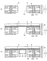
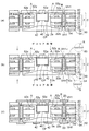
図1〜図9は実施形態の電子部品内蔵基板の製造方法を示す図、図10は実施形態の電子部品内蔵基板を示す図である。以下、電子部品内蔵基板の製造方法を説明しながら、電子部品内蔵基板の構造を説明する。 1 to 9 are diagrams showing a method of manufacturing an electronic component built-in substrate according to the embodiment, and FIG. 10 is a diagram showing the electronic component built-in substrate according to the embodiment. Hereinafter, the structure of the electronic component built-in substrate will be described while explaining the method for manufacturing the electronic component built-in substrate.
実施形態の電子部品内蔵基板の製造方法では、最初に、コア材及び配線層を備えたコア配線基板を作成する。詳しく説明すると、図1(a)に示すように、まず、厚みが200μm程度の第1コア材11の両面側に銅箔21aがそれぞれ積層された銅張積層板5を用意する。第1コア材11としては、ガラスエポキシ樹脂などの樹脂からなる絶縁材料が使用される。
In the method of manufacturing an electronic component built-in substrate according to the embodiment, first, a core wiring substrate including a core material and a wiring layer is created. More specifically, as shown in FIG. 1A, first, a
次いで、図1(b)に示すように、銅張積層板5の両面側の銅箔21aをフォトリソグラフィ及びウェットエッチングによってパターニングすることにより、両面側に第1配線層21をそれぞれ形成する。第1配線層21の厚みは18μm〜35μm程度である。
Next, as shown in FIG. 1B, the
続いて、図1(c)に示すように、第1コア材11の下面に第2コア材12と銅箔22aとを積層する。また同時に、第1コア材の上面に第3コア材13と銅箔22aとを積層する。第2コア材12及び第3コア材13の各厚みは、100μm程度である。
Subsequently, as shown in FIG. 1C, the
第2コア材12及び第3コア材13は、プリプレグを加熱・加圧することより形成される。プリプレグは、ガラスクロスなどにエポキシ樹脂などの樹脂を含侵させた半硬化状態の樹脂からなるシート状の中間材料である。
The
次いで、図1(d)に示すように、図1(c)の積層体をレーザやドリルなどによって厚み方向に貫通加工することにより、スルーホールTHを形成する。スルーホールTHの直径は200〜300μm程度に設定される。 Next, as shown in FIG. 1 (d), the through hole TH is formed by penetrating the laminated body of FIG. 1 (c) in the thickness direction with a laser or a drill. The diameter of the through hole TH is set to about 200 to 300 μm.
その後に、図2(a)に示すように、両面側の銅箔22aの上及びスルーホールTHの内面に無電解めっき及び電解めっきにより銅などからなるスルーホールめっき層22bを形成する。さらに、スルーホールTHの残りの孔にエポキシ樹脂などの樹脂体Rを充填する。
Thereafter, as shown in FIG. 2A, a through-
続いて、図2(b)に示すように、無電解めっき及び電解めっきにより、両面側のスルーホールめっき層22b及び樹脂体Rの上に銅などからなる金属めっき層22cをそれぞれ形成する。
Subsequently, as shown in FIG. 2B, a
さらに、図2(b)の積層体の両面側において、フォトリソグラフィ及びウェットエッチングにより、金属めっき層22c、スルーホールめっき層22b及び銅箔22aをそれぞれパターニングする。
Further, the
これにより、図2(c)に示すように、両面側の第2、第3コア材12,13の上に第2配線層22がそれぞれ形成される。2配線層22の厚みは、18μm〜35μm程度に設定される。
As a result, as shown in FIG. 2C, the
図2(c)の部分拡大断面図に示すように、第2配線層22は、下から順に、銅箔22a、スルーホールめっき層22b及び金属めっき層22cが積層されて形成される。両面側の第2配線層22は、スルーホールめっき層22bを介して相互接続される。
2C, the
以上により、本実施形態で使用されるコア配線基板2が得られる。図2(c)に示すように、コア配線基板2では、第1コア材11と、その両面側に配置された第2コア材12及び第3コア材13とによりコア基板3が形成される。第1コア材11の両面側に第1配線層21がそれぞれ形成されている。
As described above, the
コア基板3の両面側には第2配線層22がそれぞれ形成されている。さらに、コア基板3には厚み方向に貫通するスルーホールTHが形成されている。両面側の第2配線層22はスルーホールTHの側壁に形成されたスルーホールめっき層22bを介して電気的に相互接続されている。スルーホールTH内の孔には樹脂体Rが充填されている。また、第1コア材11の下面の第1配線層21がスルーホールめっき層22bに電気的に接続されている。
Second wiring layers 22 are respectively formed on both sides of the
なお、図2(c)の例では、スルーホールTH内の孔に樹脂体Rが充填されているが、スルーホールTH内の全体が銅などの金属めっき層で埋め込まれていてもよい。また、配線層の積層数も任意に設定することができる。 In the example of FIG. 2C, the resin body R is filled in the hole in the through hole TH, but the entire inside of the through hole TH may be embedded with a metal plating layer such as copper. Further, the number of wiring layers can be arbitrarily set.
以上のようにして、本実施形態では、コア基板3と、その内部及び両面に形成された第1、第2配線層21,22とを備えたコア配線基板2を作成する。第1、第2配線層21,22は、所要の電気回路を構築して形成される。
As described above, in the present embodiment, the
次に、コア配線基板2に電子部品を内蔵する方法について説明する。図3(a)に示すように、まず、金型を使用するパンチングによって、図2(c)のコア配線基板2の中央部に上面から下面まで貫通する開口部2aを形成する。パンチングの代わりに、レーザ加工やドリル加工により開口部2aを形成してもよい。開口部2aはキャビティとも呼ばれる。
Next, a method for incorporating electronic components in the
コア配線基板2の開口部2aは平面視して例えば四角形状で形成され、後述するように開口部2a内に電子部品が配置される。多面取り用の大型のコア配線基板2を使用する場合は、複数で画定された製品領域に開口部2aがそれぞれ配置される。
The
このとき、開口部2aの外側周囲領域のコア配線基板2に、第2配線層22が外側に後退して第3コア材13の上面が露出する露出面Aが配置されるように、開口部2aが形成される。露出面Aは、開口部2aに沿ってその外側周囲領域に環状に配置される。
At this time, the opening portion is arranged so that the exposed surface A in which the
次いで、図3(b)に示すように、コア配線基板2の上面に、仮止めテープ30を貼り付ける。仮止めテープ30は、樹脂を硬化させる際の加熱処理に耐える必要があるため、200℃以上の耐熱性を有するものが使用される。図3(b)以下の図面では、基板の一方の面としてコア配線基板2の下面を例示し、基板の他方の面として上面を例示する。
Next, as shown in FIG. 3B, a
そのような仮止めテープ30としては、ポリイミド又はPETなどの耐熱性の高いフィルム32の片面に粘着層34が積層されたものが使用される。粘着層34は例えばポリイミドからなる。そして、仮止めテープ30の粘着層34の面をコア配線基板2の上面に仮接着させる。
As such a
本実施形態では、搭載される電子部品を樹脂で封止する際に、樹脂の充填圧力で電子部品の位置ずれや傾きが生じないように、接着力の強い粘着層34を有する仮止めテープ30が採用される。
In this embodiment, when the electronic component to be mounted is sealed with a resin, the
続いて、図3(c)に示すように、コア配線基板2の開口部2a内の仮止めテープ30にチップキャパシタ40を仮接着して配置する。コア配線基板2の開口部2aの面積は、内蔵されるチップキャパシタ40の面積より一回り大きな面積で形成されている。
Subsequently, as shown in FIG. 3C, the
チップキャパシタ40は、横方向の両端側に一対の接続端子42を備えており、一対の接続端子42がコア配線基板2の表面と平行な水平方向に配置される。
The
チップキャパシタ40の接続端子42は両側面から上下面の端部まで延在して形成されている。図3(c)の例では、チップキャパシタ40の全体の厚みは、コア配線基板2の全体の厚みより薄く設定されている。あるいは、チップキャパシタ40の全体の厚みが、コア配線基板2の全体の厚みと同じに設定されるようにしてもよい。
The
チップキャパシタ40の一例としては、直方体からなるキャパシタ本体の長手方向の両端に電極が設けられたセラミックチップキャパシタがある。
As an example of the
電子部品として、チップキャパシタ40を例示するが、半導体チップ、抵抗素子、インダクタ素子などの接続端子を備えた各種の電子部品を使用することができる。また、コア配線基板2の1つの開口部2aに複数の電子部品を配置してもよい。
Although the
次いで、図4(a)に示すように、半硬化状態(Bステージ)の厚みが25〜40μm程度の樹脂フィルム52aを用意し、熱プレス機能を備えた真空ラミネーターによってコア配線基板2の下面に樹脂フィルム52aを積層する。
Next, as shown in FIG. 4A, a
このとき、130℃〜150℃の温度で熱プレスすることにより、樹脂フィルム52aの樹脂を流動化し、開口部2a内に流入させた後に、180℃〜200℃の温度で本キュアする。樹脂フィルム52aとして、熱硬化性のエポキシ樹脂又はポリイミド樹脂などが使用される。
At this time, the resin of the
これにより、図4(b)に示すように、コア配線基板2の下面に第1内側絶縁層52が形成される。チップキャパシタ40とコア配線基板2の開口部2aの側面との隙間が第1内側絶縁層52の充填絶縁部52xで埋め込まれ、チップキャパシタ40が第1内側絶縁層52によって封止された状態となる。
As a result, as shown in FIG. 4B, the first inner insulating
本実施形態では、仮止めテープ30の粘着層34の接着力を強くしているため、チップキャパシタ40が樹脂の充填圧力に耐えることができ、チップキャパシタ40の位置ずれや傾きが生じることが防止される。
In this embodiment, since the adhesive force of the
このとき、図4(b)のチップキャパシタ40の上部の外側領域に注目すると、図3(a)で説明した第3コア材13の環状の露出面Aと仮止めテープ30の下面との間の領域に第1内側絶縁層52の補強絶縁部52yが同時に充填される。これと同時に、チップキャパシタ40の接続端子42間の仮止めテープ30との間隙にも第1内側絶縁層52が充填されて、別の補強絶縁部52zが形成される。
At this time, when attention is paid to the outer region at the top of the
その後に、図5(a)に示すように、仮止めテープ30をコア配線基板2及びチップキャパシタ40から剥離する。このとき、チップキャパシタ40は、その上及び外側周囲領域の補強絶縁部52y,53zによってコア配線基板2に強く固定されている。
Thereafter, as shown in FIG. 5A, the
このため、仮止めテープ30の粘着層34の接着力が強い場合であっても、チップキャパシタ40が仮止めテープ30と共に充填絶縁部52xから抜けて脱落することが防止される。
For this reason, even if the adhesive force of the
図5(b)は図5(a)の様子を上側からみた部分平面図である。図5(b)に示すように、チップキャパシタ40はコア配線基板2の四角状の開口部2aの中に配置され、チップキャパシタ40と開口部2aの側面との間に充填絶縁部52xが形成されている。
FIG. 5B is a partial plan view of the state of FIG. As shown in FIG. 5B, the
また、開口部2aの外側周囲領域の第3コア材13の露出面Aの上及びチップキャパシタ40の上に、充填絶縁部52xに繋がる補強絶縁部52y,52zが形成されている。
Further, on the exposed surface A of the
補強絶縁部52yの外側領域に第2配線層22のプレーン層22xが一体的に形成されている。プレーン層22xは、電源プレーン又はグランドプレーンとして形成される。プレーン層22xは、スルーホールめっき層22bを介して、下面側の第2配線層22に電気的に接続されている。
A
また、プレーン層22xには円状の開口部22zが形成されており、その開口部22z内に第2配線層22の接続パッド22yがプレーン層22xと分離された状態で配置されている。接続パッド22yはスルーホールめっき層22bを介して、下面側の第2配線層22に電気的に接続されている。
Further, a
また、本実施形態のように、チップキャパシタ40の厚みがコア配線基板2の厚みより薄い場合は、コア配線基板2の開口部2a内のチップキャパシタ40を樹脂で封止する際に、樹脂を埋め込む空間の体積が大きい構造となる。
In addition, when the thickness of the
このため、図5(a)に示すように、コア配線基板2の開口部2aの領域の第1内側絶縁層52は、チップキャパシタ40側に落ち込む窪み部CPとなって形成される。このように、コア配線基板2の開口部2aに配置されたチップキャパシタ40を第1内側絶縁層52で封止する際に、第1内側絶縁層52の下面に内部にへこむ窪み部CPが発生してしまう。第1内側絶縁層52に窪み部CPが発生していると、その上に微細な配線層を歩留りよく形成することは困難である。
For this reason, as shown in FIG. 5A, the first inner insulating
例えば、セミアディティブ法で配線層を形成する場合は、シード層の上にドライフィルムレジスト層をパターニングする際に、レジストパターン層が窪み部CP上で浮いて配置されるため、隣接する配線層が下側で繋がって形成される不具合が発生する。 For example, when the wiring layer is formed by the semi-additive method, when patterning the dry film resist layer on the seed layer, the resist pattern layer is arranged so as to float on the recessed portion CP. There is a problem of being connected on the lower side.
この対策として、本実施形態では、図6(a)に示すように、コア配線基板2の下面に平坦化用の樹脂フィルム54aを積層する。また同時に、コア配線基板2の上面に樹脂フィルム60aを積層する。樹脂フィルム54a,60aとして、熱硬化性のエポキシ樹脂又はポリイミド樹脂などが使用される。
As a countermeasure, in this embodiment, as shown in FIG. 6A, a
そして、前述した第1内側絶縁層52の形成方法と同様に、熱プレス機能を備えた真空ラミネーターによって、130℃〜150℃の温度で熱プレスして両面側の樹脂フィルム54a,60aを流動化させた後に、180℃〜200℃の温度で本キュアする。
Then, similarly to the method for forming the first inner insulating
これにより、図6(b)に示すように、コア配線基板2の下面の第1内側絶縁層52の上に第1外側絶縁層54が積層されて形成される。このとき、コア配線基板2の下面では、第1内側絶縁層52の窪み部CPが第1外側絶縁層54で充填されて平坦化される。このようにして、第1外側絶縁層54の下面が平坦面となって形成される。
Thereby, as shown in FIG. 6B, the first outer insulating
以上により、コア配線基板2の下面に、チップキャパシタ40を埋め込む第1内側絶縁層52とそれを被覆する第1外側絶縁層54とから第1絶縁層50が形成される。
As described above, the first insulating
また同時に、コア配線基板2の上面に、コア配線基板2、チップキャパシタ40及び補強絶縁部52y,52zの上に第2絶縁層60が形成される。
At the same time, the second insulating
第1外側絶縁層54は、上記したように第1内側絶縁層52の窪み部CPを平坦化する目的以外に、両面側の絶縁層の表面粗さを同一に設定するために形成される。
The first outer insulating
ここで、本実施形態と違って、第1内側絶縁層52の上に第1外側絶縁層54を形成しない場合は、第2絶縁層60を形成する際に、第1内側絶縁層52の表面がさらに加熱処理されて第2絶縁層60より強固に硬化した状態となる。
Here, unlike the present embodiment, when the first outer insulating
このため、デスミア処理で配線層のアンカー用の粗化面を形成する際に、第2絶縁層60の表面はエッチングによって十分に凹凸が形成されて所要の粗化面となるが、第1内側絶縁層52の表面はエッチングされにくいため、十分に粗化されない。
For this reason, when the roughened surface for the anchor of the wiring layer is formed by the desmear process, the surface of the second insulating
よって、第1内側絶縁層52の下面は十分に粗化されていないため、配線層を形成する際に十分な密着性が得られなくなる。
Therefore, since the lower surface of the first inner insulating
そこで、コア配線基板2の上面に第2絶縁層60を形成すると同時に、コア配線基板2の下面の第1内側絶縁層52の上に第1外側絶縁層54を形成する。これにより、第1外側絶縁層54と第2絶縁層60とは同じ熱履歴となる。
Therefore, the second insulating
このため、両面側の第1外側絶縁層54と第2絶縁層60の各表面に、同一スペックの十分な表面粗さの粗化面をそれぞれ形成することができる。
For this reason, the rough surface of sufficient surface roughness of the same specification can be formed in each surface of the 1st outer
第1絶縁層50の厚みと第2絶縁層60の厚みの差は、±20%以下の範囲内、好適には±10%以下の範囲内に設定されていることが望ましく、さらに好適には、両者の厚みが略同一に設定される。第1絶縁層50と第2絶縁層60とを略同一の厚みにする場合は、例えば以下のように設定される。
The difference between the thickness of the first insulating
前述した図6(b)において、第1絶縁層50の厚みとして、第1内側絶縁層52の厚みを10μmとし、第1外側絶縁層54の厚みを20μmとする場合は、図6(b)の第2絶縁層60の厚みは30μmに設定される。第1絶縁層50の厚みは、第2配線層22上から第1絶縁層50の表面までの厚みである。また、第2絶縁層52の厚みは、第2配線層22上から第2絶縁層52の表面までの厚みである。
In FIG. 6B, when the thickness of the first insulating
コア配線基板2の両面側の第1、第2絶縁層50,60の各厚みを同じにすることにより、反りに強い構造となる。なお、絶縁層として絶縁樹脂を例示するが、その他の絶縁材料を使用することも可能である。
By making the thicknesses of the first and second insulating
次いで、図7(a)に示すように、コア配線基板2の上面側の第2絶縁層60をレーザなどで加工することにより、第1ビアホールVH1を形成する。第1ビアホールVH1は、チップキャパシタ40の接続端子42及び第2配線層22の接続部の上にそれぞれ到達して配置される。
Next, as shown in FIG. 7A, the first via hole VH1 is formed by processing the second insulating
また同時に、コア配線基板2の下面側の第1外側絶縁層54及び第1内側絶縁層52をレーザなどで加工することにより、第2配線層22に到達する第1ビアホールVH1を形成する。
At the same time, the first outer insulating
その後に、図7(b)に示すように、コア配線基板2の両面側において、過マンガン酸カリウム溶液などで第1ビアホールVH1内をデスミア処理することにより、第1ホールVH1の底に残留する樹脂スミアをクリーニングする。
Thereafter, as shown in FIG. 7B, the inside of the first via hole VH1 is desmeared with a potassium permanganate solution or the like on both sides of the
このとき同時に、図7(b)の部分拡大断面図に示すように、デスミア処理によって、両面側の第1外側絶縁層54及び第2絶縁層60の各表面に凹凸が形成されて表面が粗化面Rとなる。
At the same time, as shown in the partially enlarged cross-sectional view of FIG. 7B, the surface of the first outer insulating
第1外側絶縁層54及び第2絶縁層60の各粗化面Rの表面粗さ(Ra)は、500nm以下、好適には100nm〜400nmに設定される。
The surface roughness (Ra) of each roughened surface R of the first outer insulating
前述したように、第1外側絶縁層54及び第2絶縁層60の熱履歴は、この時点ではそれらを形成する際の加熱処理のみで同一であるため、第1外側絶縁層54及び第2絶縁層60には同一スペックの表面粗さの適度な粗化面Rが形成される。
As described above, since the thermal history of the first outer insulating
後述する他の絶縁層においても、表面粗さは第1外側絶縁層54及び第2絶縁層60と同一範囲に設定される。
Also in other insulating layers described later, the surface roughness is set in the same range as the first outer insulating
デスミア処理の方法として、過マンガン酸法を例示したが、プラズマエッチング、又はブラスト処理などを使用してもよい。プラズマエッチングを使用する場合は、例えば、CF4にO2又はN2などが添加された混合ガスを使用するドライエッチング装置によって行われる。 Although the permanganic acid method has been exemplified as the desmear treatment method, plasma etching, blast treatment, or the like may be used. In the case of using plasma etching, for example, it is performed by a dry etching apparatus using a mixed gas in which O 2 or N 2 or the like is added to CF 4 .
さらに、図7(c)に示すように、コア配線基板2の上面側において、第1ビアホールVH1内のビア導体を介してチップキャパシタ40の接続端子42及び第2配線層22に接続される第3配線層23を第2絶縁層60の上に形成する。
Further, as shown in FIG. 7C, on the upper surface side of the
また同時に、コア配線基板2の下面側において、第1ビアホールVH1内のビア導体を介して第2配線層22に接続される第3配線層23を第1絶縁層50の上に形成する。
At the same time, a
第1外側絶縁層54及び第2絶縁層60の各表面は適度に粗化されているため、第3配線層23はアンカー効果によって密着性よく第1外側絶縁層54及び第2絶縁層60の上にそれぞれ形成される。
Since the surfaces of the first outer insulating
第3配線層23は、例えば、セミアディティブ法によって形成される。詳しく説明すると、コア配線基板2の上面側では、まず、第2絶縁層60の上及び第1ビアホールVH1の内面に無電解めっき又はスパッタ法により銅などからなるシード層(不図示)を形成する。
The
次いで、第3配線層23が配置される部分に開口部が設けられためっきレジスト層(不図示)をシード層の上にフォトリソグラフィに基づいて形成する。さらに、シード層をめっき給電経路に利用する電解めっきにより、第1ビアホールVH1内からめっきレジスト層の開口部に銅などからなる金属めっき層(不図示)を形成する。
Next, a plating resist layer (not shown) provided with an opening in a portion where the
続いて、めっきレジスト層を除去した後に、金属めっき層をマスクにしてシード層をエッチングして除去する。これにより、シード層及び金属めっき層から第3配線層23が得られる。
Subsequently, after removing the plating resist layer, the seed layer is etched and removed using the metal plating layer as a mask. Thereby, the
前述したように、コア配線基板2の両面側の第1、第2絶縁層50,60との各厚みを同じに設定すると、両面側で第1ビアホールVH1の深さや形状が同一になる。このため、同一の電解めっき条件で、両面側の第1ビアホールVH1に金属めっき層を信頼性よく埋め込むことができる。
As described above, when the thicknesses of the first and second insulating
コア配線基板2の下面側においても、同様な方法で第3配線層23が同時に形成される。
Also on the lower surface side of the
他の配線層においても、好適には、セミアディティブ法で形成されるが、サブトラクティブ法又はフルアディティブ法などの他の配線形成方法を使用してもよい。 Other wiring layers are preferably formed by a semi-additive method, but other wiring forming methods such as a subtractive method or a full additive method may be used.
本実施形態では、コア配線基板2に所要の電気回路を構築する第1、第2配線層21,22が形成されている。このため、チップキャパシタ40とコア配線基板2の第2配線層22とを、その上の第2絶縁層60に形成された第1ビアホールVH1を経由する第3配線層23によって容易に接続することができる。
In the present embodiment, first and second wiring layers 21 and 22 for forming a required electric circuit are formed on the
なお、図7(b)及び(c)において、コア基板3の下面側の第1絶縁層50に第1ビアホールVHを形成する際に、チップキャパシタ40の下側の接続端子42に到達する第1ビアホールを同時に形成してもよい。そして、第1絶縁層50上に形成された第3配線層23が第1ビアホール内のビア導体を介してチップキャパシタ40の接続端子42に接続された形態としてもよい。
7B and 7C, when the first via hole VH is formed in the first insulating
次いで、図8(a)に示すように、前述した図6(b)〜図7(b)と同様な工程を繰り返す。これにより、コア配線基板2の両面側において、第3配線層23の接続部上に第2ビアホールVH2を備えた第3絶縁層70を第1絶縁層50及び第2絶縁層60の上にそれぞれ形成成する。
Next, as shown in FIG. 8A, the same steps as those in FIGS. 6B to 7B are repeated. Thereby, the third insulating
さらに、図8(b)に示すように、前述した図7(c)と同様な方法により、コア配線基板2の両面側において、第2ビアホールVH2内のビア導体を介して第3配線層23に接続される第4配線層24を第3絶縁層70の上にそれぞれ形成する。
Further, as shown in FIG. 8B, the
続いて、図9に示すように、前述した図6(b)〜図7(b)と同様な方法により、コア配線基板2の両面側において、第4配線層24の接続部上に第3ビアホールVH3を備えた第4絶縁層80を第3絶縁層70の上にそれぞれ形成成する。
Subsequently, as shown in FIG. 9, the third method is performed on the connection portion of the
さらに、同じく図9に示すように、前述した図7(c)と同様な方法により、コア配線基板2の両面側において、第3ビアホールVH3内のビア導体を介して第4配線層24に接続される第5配線層25を第4絶縁層80の上にそれぞれ形成する。
Further, as shown in FIG. 9, in the same manner as in FIG. 7C described above, the both sides of the
その後に、図10に示すように、コア配線基板2の両面側において、第5配線層25の接続部上に開口部82aが設けられたソルダレジスト層82を第4絶縁層80の上にそれぞれ形成する。
After that, as shown in FIG. 10, on both sides of the
以上により、実施形態の電子部品内蔵基板1が得られる。なお、多面取り用の大型のコア配線基板2を使用する場合は、各製品領域から個々の電子部品内蔵基板1が得られるように分割される。
Thus, the electronic component built-in substrate 1 of the embodiment is obtained. In addition, when using the large
図10に示すように、実施形態の電子部品内蔵基板1では、厚み方向の中央部に前述した図3(c)で説明したコア配線基板2が配置され、そのコア配線基板2の中央部に厚み方向に貫通する開口部2aが設けられている。
As shown in FIG. 10, in the electronic component built-in substrate 1 of the embodiment, the
コア配線基板2では、第1コア材11の両面に第2コア材12及び第3コア13が配置されてコア基板3が形成されている。第1コア材11の両面に第1配線層21がそれぞれ形成されている。また、コア基板3の両面に第2配線層22がそれぞれ形成されている。
In the
両面側の第2配線層22は、スルーホールTH内のスルーホールめっき層22bを介して相互接続されている。第1、第2配線層21,22は所要の電気回路を構築するように形成されている。
The second wiring layers 22 on both sides are interconnected via a through-
また、前述した図3(a)で説明したように、開口部2aの外側周囲領域のコア配線基板2に、第2配線層22が外側に後退して第3コア材13の上面が露出する露出面Aが配置されている。
Further, as described with reference to FIG. 3A described above, the
そして、コア配線基板2の開口部2a内に、両端側に一対の接続端子42を備えたチップキャパシタ40が配置されている。チップキャパシタ40は、一対の接続端子42が水平方向に並ぶようにして配置されている。チップキャパシタ40の厚みはコア配線基板2の厚みより薄く設定されており、チップキャパシタ40は開口部2a内の上寄りの部分に配置されている。
A
コア配線基板2の下面にはチップキャパシタ40を封止する第1内側絶縁層52が形成されている。第1内側絶縁層52は、チップキャパシタ40とコア配線基板2の開口部2aの側面との間からチップキャパシタ40の下側の領域を充填する充填絶縁部52xを備えて形成されている。
A first inner insulating
また、コア配線基板2の上面には第2絶縁層60が形成されている。そして、第1内側絶縁層52は、開口部2aの外側周囲領域の第3コア材13の露出面Aと第2絶縁層60との間、及びチップキャパシタ40と第2絶縁層60との間に、充填絶縁部52xに繋がる補強絶縁部52y,52zを備えて形成されている。
A second insulating
さらに、第1内側絶縁層52の下面に第1外側絶縁層54が形成されている。第1外側絶縁層54の下面は全体にわたって平坦化されて形成されている。第1内側絶縁層52と第1外側絶縁層54とから第1絶縁層50が形成される。
Further, a first outer insulating
また、両面側の第1絶縁層50及び第2絶縁層60には、第2配線層22に到達する第1ビアホールVH1がそれぞれ形成されている。
Further, first via holes VH1 reaching the
さらに、両面側の第1絶縁層50及び第2絶縁層60の上には、第1ビアホールVH1内のビア導体を介して第2配線層22に接続される第3配線層23がそれぞれ形成されている。コア配線基板2の上面側では、チップキャパシタ40の接続端子42が第3配線層23及び第1ビアホールVH1内のビア導体によってコア配線基板2の第2配線層22に電気的に接続されている。
Further, a
また同様に、両面側の第1絶縁層50及び第2絶縁層60の上には、第3配線層23に到達する第2ビアホールVH2を備えた第3絶縁層70が形成されている。さらに、両面側の第3絶縁層70の上には、第2ビアホールVH2内のビア導体を介して第3配線層23に接続される第4配線層24がそれぞれ形成されている。
Similarly, a third insulating
また同様に、両面側の第3絶縁層70の上には、第4配線層24に到達する第3ビアホールVH3を備えた第4絶縁層80が形成されている。また、両面側の第4絶縁層80の上には、第3ビアホールVH3内のビア導体を介して第4配線層24に接続される第5配線層25がそれぞれ形成されている。
Similarly, a fourth insulating
さらに、両面側の第4絶縁層80の上に、第5配線層25の接続部上に開口部82aが設けられたソルダレジスト層82がそれぞれ形成されている。
Further, a solder resist
本実施形態の電子部品内蔵基板1では、コア配線基板2の開口部2aに配置されたチップキャパシタ40を封止する際に、チップキャパシタ40の周りを第1内側絶縁層52で埋め込んだ後に、平坦化用の第1外側絶縁層54を形成している。
In the electronic component built-in substrate 1 of the present embodiment, when the
これにより、特にチップキャパシタ40の厚みがコア配線基板2の厚みより薄い場合に、開口部2aを充填する部分の第1内側絶縁層52に窪み部CPが発生するとしても、第1外側絶縁層54で窪み部CPを平坦化することができる。
As a result, even when the
また、コア配線基板2の下面に形成された第1内側絶縁層52の下に第1外側絶縁層54を形成すると同時に、コア配線基板2の上面に第2絶縁層60を形成している。これにより、コア配線基板2の両面の第1外側絶縁層54及び第2絶縁層60は熱履歴が同一になる。
In addition, the first outer insulating
従って、第1外側絶縁層54及び第2絶縁層60に十分な表面粗さの粗化面を形成することができるので、第1外側絶縁層54及び第2絶縁層60の上に微細な第3配線層23を歩留りよく形成することができる。
Accordingly, a roughened surface having a sufficient surface roughness can be formed on the first outer insulating
また、本実施形態の電子部品内蔵基板1では、コア配線基板2が所要の電気回路を構築する第1、第2配線層21,22を備えている。コア配線基板2の上面の第2配線層22はチップキャパシタ40の接続端子42の横方向の隣接する領域に配置されている。
Further, in the electronic component built-in substrate 1 of the present embodiment, the
これにより、チップキャパシタ40の接続端子42とコア配線基板2の第2配線層22とを、その上の第2絶縁層60に形成された第1ビアホールVH1を経由する第3配線層23によって容易に接続することができる。
Thereby, the
また、好適な形態では、コア配線基板2の下面に形成されてチップキャパシタ40を封止する第1絶縁層50と、コア配線基板2の上面に形成される第2絶縁層60との間で、厚みを同一に設定している。これにより、反りに強い構造となると共に、両面側の第1ビアホールVH1に金属めっき層を同一めっき条件で安定して埋め込むことができる。
Further, in a preferred embodiment, between the first insulating
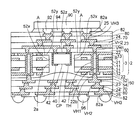
図11には、図10の電子部品内蔵基板1に半導体チップが実装された様子が示されている。図11に示すように、図10の電子部品内蔵基板1の上面側の第5配線層25に、半導体チップ90の接続部がはんだなどのバンプ電極92を介してフリップチップ接続される。
FIG. 11 shows a state in which a semiconductor chip is mounted on the electronic component built-in substrate 1 of FIG. As shown in FIG. 11, the connection portion of the
その後に、半導体チップ90と電子部品内蔵基板1との隙間にアンダーフィル樹脂94が充填される。このように、図10の電子部品内蔵基板1の第2絶縁層22側の最外面が半導体チップ90を搭載するための部品搭載面として形成される。
Thereafter, an
さらに、電子部品内蔵基板1の下面側の第5配線層25(パッド)にはんだボールを搭載するなどして外部接続端子96を形成する。
Further, the
図11の例では、電子部品内蔵基板1のチップキャパシタ40は、半導体チップ90の電源電圧を安定させ、かつ高周波ノイズを低減させる目的で電源ラインとグランドラインとの間にデカップリングキャパシタとして配置される。
In the example of FIG. 11, the
本実施形態では、チップキャパシタ40を内蔵させ、表面に半導体チップ90を実装する組み合わせを例示したが、各種の電子部品の組み合わせに適用することができる。また、コア基板に配線層が形成されていない形態にも適用することができる。
In the present embodiment, the combination in which the
1…電子部品内蔵基板、2…コア配線基板、3…コア基板、5…銅張積層板、2a,22z,82a…開口部、11…第1コア材、12…第2コア材、13…第3コア材、21…第1配線層、22…第2配線層、23…第3配線層、24…第5配線層、25…第5配線層、21a,22a…銅箔、22b…スルーホールめっき層、22c…金属めっき層、22x…プレーン層、22y…接続パッド、30…仮止めテープ、32…フィルム、34…粘着層、40…チップキャパシタ、42…接続端子、50…第1絶縁層、52…第1内側絶縁層、52x…充填絶縁部、52y,52z…補強絶縁部、54…第1外側絶縁層、52a,54a,60a…樹脂フィルム、60…第2絶縁層、70…第3絶縁層、80…第4絶縁層、82…ソルダレジスト層、90…半導体チップ、92…バンプ電極、94…アンダーフィル樹脂、96…外部接続端子、A…露出面、CP…窪み部、R…樹脂体、TH…スルーホール。VH1…第1ビアホール、VH2…第2ビアホール、VH3…第3ビアホール。
DESCRIPTION OF SYMBOLS 1 ... Electronic component built-in board, 2 ... Core wiring board, 3 ... Core board, 5 ... Copper clad laminated board, 2a, 22z, 82a ... Opening part, 11 ... 1st core material, 12 ... 2nd core material, 13 ... 3rd core material, 21 ... 1st wiring layer, 22 ... 2nd wiring layer, 23 ... 3rd wiring layer, 24 ... 5th wiring layer, 25 ... 5th wiring layer, 21a, 22a ... Copper foil, 22b ... Through Hole plating layer, 22c ... metal plating layer, 22x ... plane layer, 22y ... connection pad, 30 ... temporary fastening tape, 32 ... film, 34 ... adhesive layer, 40 ... chip capacitor, 42 ... connection terminal, 50 ...
Claims (12)
前記基板に形成された第1配線層と、
前記開口部内に配置された電子部品と、
前記基板の一方の面に形成され、前記電子部品を封止する第1絶縁層と、
前記基板の他方の面に形成された第2絶縁層と、
前記第1絶縁層上に形成された第2配線層と、
前記第2絶縁層上に形成された第3配線層と
を有し、
前記第1絶縁層は、前記基板の一方の面を被覆して前記開口部内を充填する内側絶縁層と、前記内側絶縁層上に形成された外側絶縁層とから形成されていることを特徴とする電子部品内蔵基板。 A substrate with an opening;
A first wiring layer formed on the substrate;
An electronic component disposed in the opening;
A first insulating layer formed on one surface of the substrate and encapsulating the electronic component;
A second insulating layer formed on the other surface of the substrate;
A second wiring layer formed on the first insulating layer;
A third wiring layer formed on the second insulating layer;
The first insulating layer is formed of an inner insulating layer that covers one surface of the substrate and fills the opening, and an outer insulating layer formed on the inner insulating layer. Electronic component built-in board.
前記第2配線層が、前記内側絶縁層及び外側絶縁層内に形成されたビア導体を介して前記第1配線層に接続されており、
前記第3配線層が、前記第2絶縁層内に形成されたビア導体を介して前記電子部品の接続端子及び前記第1配線層に接続されていることを特徴とする請求項1に記載の電子部品内蔵基板。 The first wiring layer is formed on both sides of the substrate,
The second wiring layer is connected to the first wiring layer via via conductors formed in the inner insulating layer and the outer insulating layer;
2. The device according to claim 1, wherein the third wiring layer is connected to a connection terminal of the electronic component and the first wiring layer through a via conductor formed in the second insulating layer. Electronic component built-in substrate.
前記開口部内に電子部品を配置する工程と、
前記基板の一方の面に前記電子部品を封止する内側絶縁層を形成する工程と、
前記内側絶縁層の上に外側絶縁層を形成して前記基板の一方の面に前記内側絶縁層及び外側絶縁層から形成される第1絶縁層を得ると共に、前記基板の他方の面に第2絶縁層を形成する工程と、
前記第1絶縁層の上に第2配線層を形成すると共に、前記第2絶縁層の上に第3配線層を形成する工程とを有することを電子部品内蔵基板の製造方法。 Preparing a substrate having a first wiring layer and forming an opening in the substrate;
Placing an electronic component in the opening;
Forming an inner insulating layer for sealing the electronic component on one surface of the substrate;
An outer insulating layer is formed on the inner insulating layer to obtain a first insulating layer formed from the inner insulating layer and the outer insulating layer on one surface of the substrate, and a second is formed on the other surface of the substrate. Forming an insulating layer;
Forming a second wiring layer on the first insulating layer and forming a third wiring layer on the second insulating layer.
前記第2配線層及び第3配線層を形成する工程において
前記第2配線層は、前記第1絶縁層内に形成されたビア導体を介して前記第1配線層に接続され、
前記第3配線層は、前記第2絶縁層内に形成されたビア導体を介して前記電子部品の接続端子及び前記第1配線層に接続されることを特徴とする請求項7に記載の電子部品内蔵基板の製造方法。 In the step of preparing the substrate and forming the opening, the first wiring layer is formed on both surfaces of the substrate,
In the step of forming the second wiring layer and the third wiring layer, the second wiring layer is connected to the first wiring layer via a via conductor formed in the first insulating layer,
8. The electron according to claim 7, wherein the third wiring layer is connected to a connection terminal of the electronic component and the first wiring layer through a via conductor formed in the second insulating layer. A method for manufacturing a component-embedded substrate.
前記内側絶縁層を形成する工程において、前記露出面の上に前記内側絶縁層の補強絶縁部が形成されることを特徴とする請求項7乃至9のいずれか一項に記載の電子部品内蔵基板の製造方法。 In the step of forming the opening in the substrate, the surface of the substrate in the outer peripheral region of the opening is an exposed surface in which the first wiring layer has receded to the outside,
10. The electronic component built-in substrate according to claim 7, wherein a reinforcing insulating portion of the inner insulating layer is formed on the exposed surface in the step of forming the inner insulating layer. Manufacturing method.
前記外側絶縁層を形成する工程において、前記窪み部を充填して前記内側絶縁層の上に前記外側絶縁層が形成されて、前記第1絶縁層の表面が平坦化されることを特徴とする請求項7乃至10のいずれか一項に記載の電子部品内蔵基板の製造方法。 In the step of forming the inner insulating layer, a recess is formed in the inner insulating layer of the portion filled in the opening,
In the step of forming the outer insulating layer, the outer insulating layer is formed on the inner insulating layer by filling the depression, and the surface of the first insulating layer is planarized. The manufacturing method of the electronic component built-in substrate as described in any one of Claims 7 thru | or 10.
Priority Applications (2)
| Application Number | Priority Date | Filing Date | Title |
|---|---|---|---|
| JP2013068549A JP6200178B2 (en) | 2013-03-28 | 2013-03-28 | Electronic component built-in substrate and manufacturing method thereof |
| US14/221,567 US9331011B2 (en) | 2013-03-28 | 2014-03-21 | Electronic component built-in substrate and method of manufacturing the same |
Applications Claiming Priority (1)
| Application Number | Priority Date | Filing Date | Title |
|---|---|---|---|
| JP2013068549A JP6200178B2 (en) | 2013-03-28 | 2013-03-28 | Electronic component built-in substrate and manufacturing method thereof |
Publications (3)
| Publication Number | Publication Date |
|---|---|
| JP2014192452A true JP2014192452A (en) | 2014-10-06 |
| JP2014192452A5 JP2014192452A5 (en) | 2016-01-28 |
| JP6200178B2 JP6200178B2 (en) | 2017-09-20 |
Family
ID=51620014
Family Applications (1)
| Application Number | Title | Priority Date | Filing Date |
|---|---|---|---|
| JP2013068549A Active JP6200178B2 (en) | 2013-03-28 | 2013-03-28 | Electronic component built-in substrate and manufacturing method thereof |
Country Status (2)
| Country | Link |
|---|---|
| US (1) | US9331011B2 (en) |
| JP (1) | JP6200178B2 (en) |
Cited By (9)
| Publication number | Priority date | Publication date | Assignee | Title |
|---|---|---|---|---|
| KR20160132763A (en) * | 2015-05-11 | 2016-11-21 | 삼성전기주식회사 | Electronic component package and method of manufacturing the same |
| KR20180012187A (en) * | 2016-07-26 | 2018-02-05 | 삼성전기주식회사 | Fan-out semiconductor package |
| JP2018064085A (en) * | 2016-10-10 | 2018-04-19 | サムソン エレクトロ−メカニックス カンパニーリミテッド. | Fan-out semiconductor package and photosensitive resin composition |
| KR20180055570A (en) * | 2016-11-17 | 2018-05-25 | 삼성전기주식회사 | Fan-out semiconductor package |
| US10199337B2 (en) | 2015-05-11 | 2019-02-05 | Samsung Electro-Mechanics Co., Ltd. | Electronic component package and method of manufacturing the same |
| KR20190023285A (en) * | 2017-08-28 | 2019-03-08 | 삼성전기주식회사 | Fan-out semiconductor package |
| US10262949B2 (en) | 2015-05-11 | 2019-04-16 | Samsung Electro-Mechanics Co., Ltd. | Fan-out semiconductor package and method of manufacturing the same |
| WO2019111873A1 (en) * | 2017-12-05 | 2019-06-13 | 株式会社村田製作所 | Module |
| CN110957281A (en) * | 2018-09-27 | 2020-04-03 | 台湾积体电路制造股份有限公司 | Integrated circuit package and method |
Families Citing this family (12)
| Publication number | Priority date | Publication date | Assignee | Title |
|---|---|---|---|---|
| KR101601815B1 (en) * | 2014-02-06 | 2016-03-10 | 삼성전기주식회사 | Embedded board, printed circuit board and method of manufactruing the same |
| US9837484B2 (en) * | 2015-05-27 | 2017-12-05 | STATS ChipPAC Pte. Ltd. | Semiconductor device and method of forming substrate including embedded component with symmetrical structure |
| US10700024B2 (en) * | 2017-08-18 | 2020-06-30 | Samsung Electro-Mechanics Co., Ltd. | Fan-out semiconductor package |
| EP3474639B1 (en) * | 2017-10-20 | 2021-07-14 | AT & S Austria Technologie & Systemtechnik Aktiengesellschaft | Embedding a component into a component carrier by transferring the component into a cavity being already filled with filling material |
| KR102005351B1 (en) * | 2017-12-07 | 2019-07-31 | 삼성전자주식회사 | Fan-out sensor package |
| KR102039711B1 (en) * | 2018-03-13 | 2019-11-01 | 삼성전자주식회사 | Fan-out component package |
| US10797017B2 (en) * | 2018-03-20 | 2020-10-06 | Unimicron Technology Corp. | Embedded chip package, manufacturing method thereof, and package-on-package structure |
| CN208691627U (en) * | 2018-08-03 | 2019-04-02 | 奥特斯科技(重庆)有限公司 | With the component load-bearing part on the component in insertion chamber and front side with double dielectric layers |
| KR102595864B1 (en) * | 2018-12-07 | 2023-10-30 | 삼성전자주식회사 | Semiconductor package |
| US10903169B2 (en) * | 2019-04-30 | 2021-01-26 | Advanced Semiconductor Engineering, Inc. | Conductive structure and wiring structure including the same |
| US11145624B2 (en) | 2019-07-26 | 2021-10-12 | Advanced Semiconductor Engineering, Inc. | Semiconductor device package and method for manufacturing the same |
| JP2021082786A (en) * | 2019-11-22 | 2021-05-27 | ルネサスエレクトロニクス株式会社 | Semiconductor device |
Citations (2)
| Publication number | Priority date | Publication date | Assignee | Title |
|---|---|---|---|---|
| JP2010114434A (en) * | 2008-10-08 | 2010-05-20 | Ngk Spark Plug Co Ltd | Component built-in wiring board and method of manufacturing the same |
| WO2010137421A1 (en) * | 2009-05-29 | 2010-12-02 | イビデン株式会社 | Wiring board and method for manufacturing same |
Family Cites Families (6)
| Publication number | Priority date | Publication date | Assignee | Title |
|---|---|---|---|---|
| JP3709882B2 (en) * | 2003-07-22 | 2005-10-26 | 松下電器産業株式会社 | Circuit module and manufacturing method thereof |
| TWI324901B (en) * | 2007-01-08 | 2010-05-11 | Unimicron Technology Corp | Printed circuit board structure integrating electronic components |
| TWI363411B (en) * | 2008-07-22 | 2012-05-01 | Advanced Semiconductor Eng | Embedded chip substrate and fabrication method thereof |
| JP5001395B2 (en) | 2010-03-31 | 2012-08-15 | イビデン株式会社 | Wiring board and method of manufacturing wiring board |
| US8895380B2 (en) * | 2010-11-22 | 2014-11-25 | Bridge Semiconductor Corporation | Method of making semiconductor assembly with built-in stiffener and semiconductor assembly manufactured thereby |
| US9406658B2 (en) * | 2010-12-17 | 2016-08-02 | Advanced Semiconductor Engineering, Inc. | Embedded component device and manufacturing methods thereof |
-
2013
- 2013-03-28 JP JP2013068549A patent/JP6200178B2/en active Active
-
2014
- 2014-03-21 US US14/221,567 patent/US9331011B2/en active Active
Patent Citations (2)
| Publication number | Priority date | Publication date | Assignee | Title |
|---|---|---|---|---|
| JP2010114434A (en) * | 2008-10-08 | 2010-05-20 | Ngk Spark Plug Co Ltd | Component built-in wiring board and method of manufacturing the same |
| WO2010137421A1 (en) * | 2009-05-29 | 2010-12-02 | イビデン株式会社 | Wiring board and method for manufacturing same |
Cited By (21)
| Publication number | Priority date | Publication date | Assignee | Title |
|---|---|---|---|---|
| US10256200B2 (en) | 2015-05-11 | 2019-04-09 | Samsung Electro-Mechanics Co., Ltd. | Electronic component package and method of manufacturing the same |
| JP2016213466A (en) * | 2015-05-11 | 2016-12-15 | サムソン エレクトロ−メカニックス カンパニーリミテッド. | Fan-out semiconductor package and manufacturing method of the same |
| KR102002071B1 (en) * | 2015-05-11 | 2019-07-22 | 삼성전자주식회사 | Fan-out semiconductor package and method of manufacturing the same |
| US10199337B2 (en) | 2015-05-11 | 2019-02-05 | Samsung Electro-Mechanics Co., Ltd. | Electronic component package and method of manufacturing the same |
| KR20160132763A (en) * | 2015-05-11 | 2016-11-21 | 삼성전기주식회사 | Electronic component package and method of manufacturing the same |
| US10262949B2 (en) | 2015-05-11 | 2019-04-16 | Samsung Electro-Mechanics Co., Ltd. | Fan-out semiconductor package and method of manufacturing the same |
| KR20180012187A (en) * | 2016-07-26 | 2018-02-05 | 삼성전기주식회사 | Fan-out semiconductor package |
| KR101994752B1 (en) * | 2016-07-26 | 2019-07-01 | 삼성전기주식회사 | Fan-out semiconductor package |
| US10283426B2 (en) | 2016-10-10 | 2019-05-07 | Samsung Electro-Mechanics Co., Ltd. | Fan-out semiconductor package and photosensitive resin composition |
| JP2018064085A (en) * | 2016-10-10 | 2018-04-19 | サムソン エレクトロ−メカニックス カンパニーリミテッド. | Fan-out semiconductor package and photosensitive resin composition |
| US10217631B2 (en) | 2016-11-17 | 2019-02-26 | Samsung Electro-Mechanics Co., Ltd. | Fan-out semiconductor package |
| KR20180055570A (en) * | 2016-11-17 | 2018-05-25 | 삼성전기주식회사 | Fan-out semiconductor package |
| KR102004801B1 (en) * | 2016-11-17 | 2019-07-29 | 삼성전기주식회사 | Fan-out semiconductor package |
| KR20190023285A (en) * | 2017-08-28 | 2019-03-08 | 삼성전기주식회사 | Fan-out semiconductor package |
| KR102029535B1 (en) * | 2017-08-28 | 2019-10-07 | 삼성전기주식회사 | Fan-out semiconductor package |
| US10685929B2 (en) | 2017-08-28 | 2020-06-16 | Samsung Electro-Mechanics Co., Ltd. | Fan-out semiconductor package |
| WO2019111873A1 (en) * | 2017-12-05 | 2019-06-13 | 株式会社村田製作所 | Module |
| US11322472B2 (en) | 2017-12-05 | 2022-05-03 | Murata Manufacturing Co., Ltd. | Module |
| CN110957281A (en) * | 2018-09-27 | 2020-04-03 | 台湾积体电路制造股份有限公司 | Integrated circuit package and method |
| US11527474B2 (en) | 2018-09-27 | 2022-12-13 | Taiwan Semiconductor Manufacturing Company, Ltd. | Integrated circuit package and method |
| CN110957281B (en) * | 2018-09-27 | 2023-06-30 | 台湾积体电路制造股份有限公司 | Integrated circuit package and method |
Also Published As
| Publication number | Publication date |
|---|---|
| US9331011B2 (en) | 2016-05-03 |
| JP6200178B2 (en) | 2017-09-20 |
| US20140291859A1 (en) | 2014-10-02 |
Similar Documents
| Publication | Publication Date | Title |
|---|---|---|
| JP6200178B2 (en) | Electronic component built-in substrate and manufacturing method thereof | |
| KR102032171B1 (en) | Electronic component built-in substrate and method of manufacturing the same | |
| JP2009200389A (en) | Method of manufacturing electronic component built-in board | |
| JP6208411B2 (en) | Wiring board and manufacturing method thereof | |
| JP6795137B2 (en) | Manufacturing method of printed circuit board with built-in electronic elements | |
| JP2010157664A (en) | Circuit substrate with electric and electronic component incorporated therein, and method of manufacturing the same | |
| TW201444440A (en) | Printed circuit board and fabricating method thereof | |
| KR20160004157A (en) | Chip embedded substrate and method of manufacturing the same | |
| JP5593863B2 (en) | Multilayer circuit board and substrate manufacturing method | |
| KR101138542B1 (en) | Manufactory method for multi-layer printed circuit board | |
| JP5385699B2 (en) | Manufacturing method of multilayer wiring board | |
| KR101205464B1 (en) | Method for manufacturing a printed circuit board | |
| JP4899409B2 (en) | Multilayer printed wiring board and manufacturing method thereof | |
| TWI477214B (en) | Printed circuit board having buried component and method for manufacturing same | |
| JP5836019B2 (en) | Component built-in substrate and manufacturing method thereof | |
| JP6266908B2 (en) | Manufacturing method of electronic component built-in substrate | |
| JP6062884B2 (en) | Component-embedded substrate, manufacturing method thereof, and mounting body | |
| TWI513392B (en) | Manufacturing method for circuit structure embedded with electronic device | |
| JP4803918B2 (en) | Manufacturing method of multilayer wiring board | |
| KR100888562B1 (en) | Method of fabricating an active device embedded printer circuit board | |
| JP4803919B2 (en) | Manufacturing method of multilayer wiring board | |
| JP2007115952A (en) | Interposer substrate and manufacturing method thereof | |
| JP6075789B2 (en) | Wiring board manufacturing method | |
| JP2000315863A (en) | Manufacture of multilayer printed wiring board | |
| JP2012191101A (en) | Manufacturing method of circuit board |
Legal Events
| Date | Code | Title | Description |
|---|---|---|---|
| A521 | Request for written amendment filed |
Free format text: JAPANESE INTERMEDIATE CODE: A523 Effective date: 20151207 |
|
| A621 | Written request for application examination |
Free format text: JAPANESE INTERMEDIATE CODE: A621 Effective date: 20151207 |
|
| A977 | Report on retrieval |
Free format text: JAPANESE INTERMEDIATE CODE: A971007 Effective date: 20161027 |
|
| A131 | Notification of reasons for refusal |
Free format text: JAPANESE INTERMEDIATE CODE: A131 Effective date: 20161206 |
|
| A521 | Request for written amendment filed |
Free format text: JAPANESE INTERMEDIATE CODE: A523 Effective date: 20170117 |
|
| TRDD | Decision of grant or rejection written | ||
| A01 | Written decision to grant a patent or to grant a registration (utility model) |
Free format text: JAPANESE INTERMEDIATE CODE: A01 Effective date: 20170808 |
|
| A61 | First payment of annual fees (during grant procedure) |
Free format text: JAPANESE INTERMEDIATE CODE: A61 Effective date: 20170825 |
|
| R150 | Certificate of patent or registration of utility model |
Ref document number: 6200178 Country of ref document: JP Free format text: JAPANESE INTERMEDIATE CODE: R150 |