JP2014142390A - 電気光学装置、電気光学装置の製造方法、及び電子機器 - Google Patents
電気光学装置、電気光学装置の製造方法、及び電子機器 Download PDFInfo
- Publication number
- JP2014142390A JP2014142390A JP2013009022A JP2013009022A JP2014142390A JP 2014142390 A JP2014142390 A JP 2014142390A JP 2013009022 A JP2013009022 A JP 2013009022A JP 2013009022 A JP2013009022 A JP 2013009022A JP 2014142390 A JP2014142390 A JP 2014142390A
- Authority
- JP
- Japan
- Prior art keywords
- contact hole
- wiring
- electrode
- liquid crystal
- insulating layer
- Prior art date
- Legal status (The legal status is an assumption and is not a legal conclusion. Google has not performed a legal analysis and makes no representation as to the accuracy of the status listed.)
- Pending
Links
- 238000000034 method Methods 0.000 title claims abstract description 36
- 238000004519 manufacturing process Methods 0.000 title claims abstract description 25
- 239000000758 substrate Substances 0.000 claims abstract description 43
- 239000003990 capacitor Substances 0.000 claims description 53
- 239000000463 material Substances 0.000 claims description 20
- 229910052751 metal Inorganic materials 0.000 claims description 12
- 239000002184 metal Substances 0.000 claims description 12
- 239000004973 liquid crystal related substance Substances 0.000 abstract description 87
- 239000010410 layer Substances 0.000 description 103
- 239000010408 film Substances 0.000 description 85
- 230000005611 electricity Effects 0.000 description 49
- 230000003068 static effect Effects 0.000 description 49
- 239000011229 interlayer Substances 0.000 description 32
- 239000004065 semiconductor Substances 0.000 description 15
- 239000003566 sealing material Substances 0.000 description 12
- VYPSYNLAJGMNEJ-UHFFFAOYSA-N silicon dioxide Inorganic materials O=[Si]=O VYPSYNLAJGMNEJ-UHFFFAOYSA-N 0.000 description 12
- 229910052814 silicon oxide Inorganic materials 0.000 description 10
- 230000015572 biosynthetic process Effects 0.000 description 7
- 230000004048 modification Effects 0.000 description 7
- 238000012986 modification Methods 0.000 description 7
- 150000002500 ions Chemical class 0.000 description 6
- 230000003287 optical effect Effects 0.000 description 6
- 238000005229 chemical vapour deposition Methods 0.000 description 5
- 229910052782 aluminium Inorganic materials 0.000 description 4
- XAGFODPZIPBFFR-UHFFFAOYSA-N aluminium Chemical compound [Al] XAGFODPZIPBFFR-UHFFFAOYSA-N 0.000 description 4
- 239000011651 chromium Substances 0.000 description 4
- 238000005530 etching Methods 0.000 description 4
- 238000005286 illumination Methods 0.000 description 4
- 238000007689 inspection Methods 0.000 description 4
- 230000010287 polarization Effects 0.000 description 4
- 239000010936 titanium Substances 0.000 description 4
- 238000002834 transmittance Methods 0.000 description 4
- 229910052581 Si3N4 Inorganic materials 0.000 description 3
- 238000010586 diagram Methods 0.000 description 3
- 239000012535 impurity Substances 0.000 description 3
- 229910010272 inorganic material Inorganic materials 0.000 description 3
- 239000011147 inorganic material Substances 0.000 description 3
- 239000011159 matrix material Substances 0.000 description 3
- HQVNEWCFYHHQES-UHFFFAOYSA-N silicon nitride Chemical compound N12[Si]34N5[Si]62N3[Si]51N64 HQVNEWCFYHHQES-UHFFFAOYSA-N 0.000 description 3
- 239000010409 thin film Substances 0.000 description 3
- VYZAMTAEIAYCRO-UHFFFAOYSA-N Chromium Chemical compound [Cr] VYZAMTAEIAYCRO-UHFFFAOYSA-N 0.000 description 2
- OAICVXFJPJFONN-UHFFFAOYSA-N Phosphorus Chemical compound [P] OAICVXFJPJFONN-UHFFFAOYSA-N 0.000 description 2
- RTAQQCXQSZGOHL-UHFFFAOYSA-N Titanium Chemical compound [Ti] RTAQQCXQSZGOHL-UHFFFAOYSA-N 0.000 description 2
- 238000006243 chemical reaction Methods 0.000 description 2
- 229910052804 chromium Inorganic materials 0.000 description 2
- 238000000151 deposition Methods 0.000 description 2
- 239000011521 glass Substances 0.000 description 2
- MRELNEQAGSRDBK-UHFFFAOYSA-N lanthanum(3+);oxygen(2-) Chemical compound [O-2].[O-2].[O-2].[La+3].[La+3] MRELNEQAGSRDBK-UHFFFAOYSA-N 0.000 description 2
- 230000003071 parasitic effect Effects 0.000 description 2
- 238000000059 patterning Methods 0.000 description 2
- 230000002093 peripheral effect Effects 0.000 description 2
- 229910052698 phosphorus Inorganic materials 0.000 description 2
- 239000011574 phosphorus Substances 0.000 description 2
- 229910021420 polycrystalline silicon Inorganic materials 0.000 description 2
- 229920005591 polysilicon Polymers 0.000 description 2
- 239000010453 quartz Substances 0.000 description 2
- 238000003860 storage Methods 0.000 description 2
- 229910052719 titanium Inorganic materials 0.000 description 2
- WFKWXMTUELFFGS-UHFFFAOYSA-N tungsten Chemical compound [W] WFKWXMTUELFFGS-UHFFFAOYSA-N 0.000 description 2
- 229910052721 tungsten Inorganic materials 0.000 description 2
- 239000010937 tungsten Substances 0.000 description 2
- ZOXJGFHDIHLPTG-UHFFFAOYSA-N Boron Chemical compound [B] ZOXJGFHDIHLPTG-UHFFFAOYSA-N 0.000 description 1
- ZOKXTWBITQBERF-UHFFFAOYSA-N Molybdenum Chemical compound [Mo] ZOKXTWBITQBERF-UHFFFAOYSA-N 0.000 description 1
- 229910004298 SiO 2 Inorganic materials 0.000 description 1
- GWEVSGVZZGPLCZ-UHFFFAOYSA-N Titan oxide Chemical compound O=[Ti]=O GWEVSGVZZGPLCZ-UHFFFAOYSA-N 0.000 description 1
- QCWXUUIWCKQGHC-UHFFFAOYSA-N Zirconium Chemical compound [Zr] QCWXUUIWCKQGHC-UHFFFAOYSA-N 0.000 description 1
- 239000000853 adhesive Substances 0.000 description 1
- 230000001070 adhesive effect Effects 0.000 description 1
- 229910045601 alloy Inorganic materials 0.000 description 1
- 239000000956 alloy Substances 0.000 description 1
- 229910052796 boron Inorganic materials 0.000 description 1
- 239000000470 constituent Substances 0.000 description 1
- 238000007599 discharging Methods 0.000 description 1
- 230000000694 effects Effects 0.000 description 1
- 239000003822 epoxy resin Substances 0.000 description 1
- 229910000449 hafnium oxide Inorganic materials 0.000 description 1
- WIHZLLGSGQNAGK-UHFFFAOYSA-N hafnium(4+);oxygen(2-) Chemical compound [O-2].[O-2].[Hf+4] WIHZLLGSGQNAGK-UHFFFAOYSA-N 0.000 description 1
- 229910052736 halogen Inorganic materials 0.000 description 1
- 150000002367 halogens Chemical class 0.000 description 1
- AMGQUBHHOARCQH-UHFFFAOYSA-N indium;oxotin Chemical compound [In].[Sn]=O AMGQUBHHOARCQH-UHFFFAOYSA-N 0.000 description 1
- 238000009413 insulation Methods 0.000 description 1
- QSHDDOUJBYECFT-UHFFFAOYSA-N mercury Chemical compound [Hg] QSHDDOUJBYECFT-UHFFFAOYSA-N 0.000 description 1
- 229910052753 mercury Inorganic materials 0.000 description 1
- 229910044991 metal oxide Inorganic materials 0.000 description 1
- 150000004706 metal oxides Chemical class 0.000 description 1
- 229910052750 molybdenum Inorganic materials 0.000 description 1
- 239000011733 molybdenum Substances 0.000 description 1
- 229910000484 niobium oxide Inorganic materials 0.000 description 1
- URLJKFSTXLNXLG-UHFFFAOYSA-N niobium(5+);oxygen(2-) Chemical compound [O-2].[O-2].[O-2].[O-2].[O-2].[Nb+5].[Nb+5] URLJKFSTXLNXLG-UHFFFAOYSA-N 0.000 description 1
- TWNQGVIAIRXVLR-UHFFFAOYSA-N oxo(oxoalumanyloxy)alumane Chemical compound O=[Al]O[Al]=O TWNQGVIAIRXVLR-UHFFFAOYSA-N 0.000 description 1
- BPUBBGLMJRNUCC-UHFFFAOYSA-N oxygen(2-);tantalum(5+) Chemical compound [O-2].[O-2].[O-2].[O-2].[O-2].[Ta+5].[Ta+5] BPUBBGLMJRNUCC-UHFFFAOYSA-N 0.000 description 1
- 238000000206 photolithography Methods 0.000 description 1
- 238000005268 plasma chemical vapour deposition Methods 0.000 description 1
- 238000005498 polishing Methods 0.000 description 1
- 229920000647 polyepoxide Polymers 0.000 description 1
- 239000003870 refractory metal Substances 0.000 description 1
- 238000000926 separation method Methods 0.000 description 1
- 229910021332 silicide Inorganic materials 0.000 description 1
- FVBUAEGBCNSCDD-UHFFFAOYSA-N silicide(4-) Chemical compound [Si-4] FVBUAEGBCNSCDD-UHFFFAOYSA-N 0.000 description 1
- 150000003377 silicon compounds Chemical class 0.000 description 1
- 125000006850 spacer group Chemical group 0.000 description 1
- 238000004528 spin coating Methods 0.000 description 1
- 239000000126 substance Substances 0.000 description 1
- 229910052715 tantalum Inorganic materials 0.000 description 1
- GUVRBAGPIYLISA-UHFFFAOYSA-N tantalum atom Chemical compound [Ta] GUVRBAGPIYLISA-UHFFFAOYSA-N 0.000 description 1
- 229910001936 tantalum oxide Inorganic materials 0.000 description 1
- 229920001187 thermosetting polymer Polymers 0.000 description 1
- OGIDPMRJRNCKJF-UHFFFAOYSA-N titanium oxide Inorganic materials [Ti]=O OGIDPMRJRNCKJF-UHFFFAOYSA-N 0.000 description 1
- 238000007740 vapor deposition Methods 0.000 description 1
- 229910052726 zirconium Inorganic materials 0.000 description 1
Images


Classifications
-
- G—PHYSICS
- G02—OPTICS
- G02F—OPTICAL DEVICES OR ARRANGEMENTS FOR THE CONTROL OF LIGHT BY MODIFICATION OF THE OPTICAL PROPERTIES OF THE MEDIA OF THE ELEMENTS INVOLVED THEREIN; NON-LINEAR OPTICS; FREQUENCY-CHANGING OF LIGHT; OPTICAL LOGIC ELEMENTS; OPTICAL ANALOGUE/DIGITAL CONVERTERS
- G02F1/00—Devices or arrangements for the control of the intensity, colour, phase, polarisation or direction of light arriving from an independent light source, e.g. switching, gating or modulating; Non-linear optics
- G02F1/01—Devices or arrangements for the control of the intensity, colour, phase, polarisation or direction of light arriving from an independent light source, e.g. switching, gating or modulating; Non-linear optics for the control of the intensity, phase, polarisation or colour
- G02F1/13—Devices or arrangements for the control of the intensity, colour, phase, polarisation or direction of light arriving from an independent light source, e.g. switching, gating or modulating; Non-linear optics for the control of the intensity, phase, polarisation or colour based on liquid crystals, e.g. single liquid crystal display cells
- G02F1/133—Constructional arrangements; Operation of liquid crystal cells; Circuit arrangements
- G02F1/136—Liquid crystal cells structurally associated with a semi-conducting layer or substrate, e.g. cells forming part of an integrated circuit
- G02F1/1362—Active matrix addressed cells
- G02F1/136204—Arrangements to prevent high voltage or static electricity failures
-
- G—PHYSICS
- G02—OPTICS
- G02F—OPTICAL DEVICES OR ARRANGEMENTS FOR THE CONTROL OF LIGHT BY MODIFICATION OF THE OPTICAL PROPERTIES OF THE MEDIA OF THE ELEMENTS INVOLVED THEREIN; NON-LINEAR OPTICS; FREQUENCY-CHANGING OF LIGHT; OPTICAL LOGIC ELEMENTS; OPTICAL ANALOGUE/DIGITAL CONVERTERS
- G02F1/00—Devices or arrangements for the control of the intensity, colour, phase, polarisation or direction of light arriving from an independent light source, e.g. switching, gating or modulating; Non-linear optics
- G02F1/01—Devices or arrangements for the control of the intensity, colour, phase, polarisation or direction of light arriving from an independent light source, e.g. switching, gating or modulating; Non-linear optics for the control of the intensity, phase, polarisation or colour
- G02F1/13—Devices or arrangements for the control of the intensity, colour, phase, polarisation or direction of light arriving from an independent light source, e.g. switching, gating or modulating; Non-linear optics for the control of the intensity, phase, polarisation or colour based on liquid crystals, e.g. single liquid crystal display cells
- G02F1/133—Constructional arrangements; Operation of liquid crystal cells; Circuit arrangements
- G02F1/136—Liquid crystal cells structurally associated with a semi-conducting layer or substrate, e.g. cells forming part of an integrated circuit
- G02F1/1362—Active matrix addressed cells
- G02F1/136213—Storage capacitors associated with the pixel electrode
-
- G—PHYSICS
- G02—OPTICS
- G02F—OPTICAL DEVICES OR ARRANGEMENTS FOR THE CONTROL OF LIGHT BY MODIFICATION OF THE OPTICAL PROPERTIES OF THE MEDIA OF THE ELEMENTS INVOLVED THEREIN; NON-LINEAR OPTICS; FREQUENCY-CHANGING OF LIGHT; OPTICAL LOGIC ELEMENTS; OPTICAL ANALOGUE/DIGITAL CONVERTERS
- G02F1/00—Devices or arrangements for the control of the intensity, colour, phase, polarisation or direction of light arriving from an independent light source, e.g. switching, gating or modulating; Non-linear optics
- G02F1/01—Devices or arrangements for the control of the intensity, colour, phase, polarisation or direction of light arriving from an independent light source, e.g. switching, gating or modulating; Non-linear optics for the control of the intensity, phase, polarisation or colour
- G02F1/13—Devices or arrangements for the control of the intensity, colour, phase, polarisation or direction of light arriving from an independent light source, e.g. switching, gating or modulating; Non-linear optics for the control of the intensity, phase, polarisation or colour based on liquid crystals, e.g. single liquid crystal display cells
- G02F1/133—Constructional arrangements; Operation of liquid crystal cells; Circuit arrangements
- G02F1/136—Liquid crystal cells structurally associated with a semi-conducting layer or substrate, e.g. cells forming part of an integrated circuit
- G02F1/1362—Active matrix addressed cells
- G02F1/136227—Through-hole connection of the pixel electrode to the active element through an insulation layer
Abstract
【解決手段】第1基材10aと、第1基材10aの上に配置されるTFT30と、TFT30に接続される、一対の電極の間に絶縁膜が挟持された容量素子116と、一対の電極のうちの一方の電極に電気的に接続される第1配線116a1と、一対の電極のうちの他方の電極に電気的に接続される第2配線116c1と、第1配線116a1と電気的に接続されるコンタクトホールCNT71aと、第2配線116c1と電気的に接続されるコンタクトホールCNT72aと、を含み、コンタクトホールCNT71a及びコンタクトホールCNT72aは、第1配線116a1及び第2配線116c1上に配置されるパッド絶縁層11eに設けられる。
【選択図】図7
Description
図1は、電気光学装置としての液晶装置が複数面付けされたウエハの一部の構成を示す模式平面図である。図2は、液晶装置の構成を示す模式平面図である。図3は、図2に示す液晶装置のH−H’線に沿う模式断面図である。図4は、液晶装置の電気的な構成を示す等価回路図である。以下、液晶装置の構成を、図1〜図4を参照しながら説明する。
図6に示すように、第1基材10a上には、チタン(Ti)やクロム(Cr)、タングステン(W)等からなる下側遮光膜3cが形成されている。下側遮光膜3cは、平面的に格子状にパターニングされており、各画素の開口領域を規定している。なお、下側遮光膜3cは、走査線3aの一部として機能するようにしてもよい。第1基材10a及び下側遮光膜3c上には、シリコン酸化膜等からなる下地絶縁層11aが形成されている。
次に、図7を参照しながら、ソース線負荷容量素子116の周辺の構造について説明する。図7に示すように、半導体層30aのデータ線側ソースドレイン領域30s(ソース領域)は、コンタクトホールCNT41とデータ線41aとコンタクトホールCNT46とを介して、ソース線負荷容量素子116を構成する第1負荷容量電極116aと電気的に接続されている。
図8及び図9は、電気光学装置としての液晶装置の製造方法のうち、ソース線負荷容量素子周辺の製造方法を示す模式断面図である。以下、液晶装置の製造方法を、図8及び図9を参照しながら説明する。なお、図8及び図9は、図7に示す液晶装置の断面構造を簡略化して説明する。
次に、本実施形態の電子機器としての投射型表示装置について、図10を参照して説明する。図10は、上記した液晶装置を備えた投射型表示装置の構成を示す概略図である。
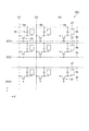
上記したように、液晶装置の構造は、図7に示すような構造であることに限定されず、例えば、図11〜図13に示すような構造でもよい。図11〜図13は、変形例の液晶装置の構造を示す模式断面図である。
上記したように、透過型の液晶装置100であることに限定されず、例えば、反射型の液晶装置に本発明を適用するようにしてもよい。
上記したように、電気光学装置として液晶装置100を用いることに限定されず、例えば、有機EL装置、プラズマディスプレイ、電子ペーパー等に適用するようにしてもよい。
Claims (7)
- 第1基材と、
前記第1基材の上に配置されるトランジスターと、
前記トランジスターのソース領域に接続される、一対の電極の間に絶縁膜が挟持された容量と、
前記一対の電極のうちの一方の電極に電気的に接続される第1配線と、
前記一対の電極のうちの他方の電極に電気的に接続される第2配線と、
前記第1基材の上から見て、前記第1配線と重なるように配置される第1コンタクトホールと、
前記第1基材の上から見て、前記第2配線と重なるように配置される第2コンタクトホールと、
を含み、
前記第1コンタクトホール及び前記第2コンタクトホールは、前記第1配線及び前記第2配線上に配置される絶縁層に設けられることを特徴とする電気光学装置。 - 請求項1に記載の電気光学装置であって、
前記第1コンタクトホールに金属膜が埋め込まれた第1電極と、
前記第2コンタクトホールに金属膜が埋め込まれた第2電極と、が設けられていることを特徴とする電気光学装置。 - 請求項2に記載の電気光学装置であって、
前記第1電極には、ソース電位が印加され、
前記第2電極には、コモン電位が印加されることを特徴とする電気光学装置。 - 第1基材の上にトランジスターを形成するトランジスター形成工程と、
前記トランジスターの上に、前記トランジスターのソース領域と接続される、一対の電極間に絶縁膜が挟持された構造の容量を形成する容量形成工程と、
前記一対の電極のうち一方の電極と電気的に接続される第1配線を形成する第1配線形成工程と、
前記一対の電極のうち他方の電極と電気的に接続される第2配線を形成する第2配線形成工程と、
前記第1配線及び前記第2配線の上に絶縁層を形成する絶縁層形成工程と、
前記絶縁層に、前記第1配線と電気的に接続するための第1コンタクトホールと、前記第2配線と電気的に接続するための第2コンタクトホールと、を形成するコンタクトホール形成工程と、
を有することを特徴とする電気光学装置の製造方法。 - 請求項4に記載の電気光学装置の製造方法であって、
前記第1コンタクトホールに金属膜を埋め込んで第1電極を形成する第1電極形成工程と、
前記第2コンタクトホールに金属膜を埋め込んで第2電極を形成する第2電極形成工程と、を有することを特徴とする電気光学装置の製造方法。 - 請求項4又は請求項5に記載の電気光学装置の製造方法であって、
前記第1電極には、ソース電位が印加され、
前記第2電極には、コモン電位が印加されることを特徴とする電気光学装置の製造方法。 - 請求項1乃至請求項3のいずれか一項に記載の電気光学装置を備えることを特徴とする電子機器。
Priority Applications (2)
| Application Number | Priority Date | Filing Date | Title |
|---|---|---|---|
| JP2013009022A JP2014142390A (ja) | 2013-01-22 | 2013-01-22 | 電気光学装置、電気光学装置の製造方法、及び電子機器 |
| US14/157,837 US9335593B2 (en) | 2013-01-22 | 2014-01-17 | Electro-optic device comprising a data line disposed between a transistor and a capacitor and electronic apparatus |
Applications Claiming Priority (1)
| Application Number | Priority Date | Filing Date | Title |
|---|---|---|---|
| JP2013009022A JP2014142390A (ja) | 2013-01-22 | 2013-01-22 | 電気光学装置、電気光学装置の製造方法、及び電子機器 |
Publications (1)
| Publication Number | Publication Date |
|---|---|
| JP2014142390A true JP2014142390A (ja) | 2014-08-07 |
Family
ID=51207413
Family Applications (1)
| Application Number | Title | Priority Date | Filing Date |
|---|---|---|---|
| JP2013009022A Pending JP2014142390A (ja) | 2013-01-22 | 2013-01-22 | 電気光学装置、電気光学装置の製造方法、及び電子機器 |
Country Status (2)
| Country | Link |
|---|---|
| US (1) | US9335593B2 (ja) |
| JP (1) | JP2014142390A (ja) |
Families Citing this family (3)
| Publication number | Priority date | Publication date | Assignee | Title |
|---|---|---|---|---|
| CN104749846B (zh) * | 2015-04-17 | 2017-06-30 | 京东方科技集团股份有限公司 | 一种阵列基板及其制作方法、显示面板 |
| CN104952934B (zh) * | 2015-06-25 | 2018-05-01 | 京东方科技集团股份有限公司 | 薄膜晶体管及制造方法、阵列基板、显示面板 |
| CN105572981B (zh) * | 2016-02-23 | 2018-05-25 | 武汉华星光电技术有限公司 | 阵列基板、显示面板以及液晶显示装置 |
Citations (7)
| Publication number | Priority date | Publication date | Assignee | Title |
|---|---|---|---|---|
| JP2005128309A (ja) * | 2003-10-24 | 2005-05-19 | Seiko Epson Corp | 電気光学装置用基板の製造方法及び電気光学装置用基板、、電気光学装置及び電子機器、並びに半導体装置用基板の製造方法及び半導体装置用基板 |
| JP2006010859A (ja) * | 2004-06-23 | 2006-01-12 | Seiko Epson Corp | 電気光学装置及び電子機器、並びに電気光学装置の製造方法 |
| JP2007041433A (ja) * | 2005-08-05 | 2007-02-15 | Seiko Epson Corp | 電気光学装置、電子機器及び電気光学装置の製造方法 |
| JP2008262136A (ja) * | 2007-04-13 | 2008-10-30 | Nec Lcd Technologies Ltd | 半透過型液晶表示装置 |
| JP2010085813A (ja) * | 2008-10-01 | 2010-04-15 | Seiko Epson Corp | 電気光学装置及び電子機器 |
| JP2011237776A (ja) * | 2010-04-12 | 2011-11-24 | Seiko Epson Corp | 電気光学装置及び電子機器 |
| JP2012108409A (ja) * | 2010-11-19 | 2012-06-07 | Seiko Epson Corp | 電気光学装置及び電子機器 |
Family Cites Families (10)
| Publication number | Priority date | Publication date | Assignee | Title |
|---|---|---|---|---|
| JPH02256030A (ja) | 1989-03-29 | 1990-10-16 | Mitsubishi Electric Corp | マトリクス型表示装置の製造方法 |
| JP4179483B2 (ja) | 1996-02-13 | 2008-11-12 | 株式会社半導体エネルギー研究所 | 表示装置の作製方法 |
| JPH10325963A (ja) | 1997-05-26 | 1998-12-08 | Sharp Corp | アクティブマトリクス型表示装置の製造方法 |
| JP5017923B2 (ja) * | 2005-08-05 | 2012-09-05 | セイコーエプソン株式会社 | 電気光学装置、及びこれを備えた電子機器 |
| CN101253618B (zh) | 2005-09-09 | 2010-12-01 | 夏普株式会社 | 薄膜元件、使用其的显示装置和存储单元、以及它们的制造方法 |
| JP2007123297A (ja) | 2005-10-24 | 2007-05-17 | Sharp Corp | 半導体装置及びその製造方法 |
| JP2008064804A (ja) | 2006-09-04 | 2008-03-21 | Ricoh Co Ltd | 画像形成装置 |
| JP2007122071A (ja) | 2006-12-04 | 2007-05-17 | Semiconductor Energy Lab Co Ltd | 表示装置の作製方法 |
| JP4306737B2 (ja) * | 2007-02-08 | 2009-08-05 | セイコーエプソン株式会社 | 電気光学装置用基板及び電気光学装置、並びに電子機器 |
| JP5786601B2 (ja) * | 2011-09-28 | 2015-09-30 | セイコーエプソン株式会社 | 電気光学装置、及び電子機器 |
-
2013
- 2013-01-22 JP JP2013009022A patent/JP2014142390A/ja active Pending
-
2014
- 2014-01-17 US US14/157,837 patent/US9335593B2/en active Active
Patent Citations (7)
| Publication number | Priority date | Publication date | Assignee | Title |
|---|---|---|---|---|
| JP2005128309A (ja) * | 2003-10-24 | 2005-05-19 | Seiko Epson Corp | 電気光学装置用基板の製造方法及び電気光学装置用基板、、電気光学装置及び電子機器、並びに半導体装置用基板の製造方法及び半導体装置用基板 |
| JP2006010859A (ja) * | 2004-06-23 | 2006-01-12 | Seiko Epson Corp | 電気光学装置及び電子機器、並びに電気光学装置の製造方法 |
| JP2007041433A (ja) * | 2005-08-05 | 2007-02-15 | Seiko Epson Corp | 電気光学装置、電子機器及び電気光学装置の製造方法 |
| JP2008262136A (ja) * | 2007-04-13 | 2008-10-30 | Nec Lcd Technologies Ltd | 半透過型液晶表示装置 |
| JP2010085813A (ja) * | 2008-10-01 | 2010-04-15 | Seiko Epson Corp | 電気光学装置及び電子機器 |
| JP2011237776A (ja) * | 2010-04-12 | 2011-11-24 | Seiko Epson Corp | 電気光学装置及び電子機器 |
| JP2012108409A (ja) * | 2010-11-19 | 2012-06-07 | Seiko Epson Corp | 電気光学装置及び電子機器 |
Also Published As
| Publication number | Publication date |
|---|---|
| US20140204301A1 (en) | 2014-07-24 |
| US9335593B2 (en) | 2016-05-10 |
Similar Documents
| Publication | Publication Date | Title |
|---|---|---|
| JP2014212191A (ja) | 半導体装置、電気光学装置、半導体装置の製造方法、電気光学装置の製造方法、及び電子機器 | |
| JP2014056212A (ja) | 電気光学装置、電気光学装置の製造方法、及び電子機器 | |
| JP6251955B2 (ja) | 電気光学装置、電気光学装置の製造方法、及び電子機器 | |
| JP2018136477A (ja) | 電気光学装置、電子機器 | |
| JP5919890B2 (ja) | 電気光学装置、及び電子機器 | |
| JP2013073032A (ja) | 液晶装置、液晶装置の製造方法、及び電子機器 | |
| JP2013182144A (ja) | 電気光学装置、及び電子機器 | |
| US9335593B2 (en) | Electro-optic device comprising a data line disposed between a transistor and a capacitor and electronic apparatus | |
| JP2014228673A (ja) | 液晶装置、液晶装置の製造方法、及び電子機器 | |
| JP2013235127A (ja) | 電気光学装置、電気光学装置の製造方法、及び電子機器 | |
| JP2017083679A (ja) | 表示装置および電子機器 | |
| JP2014182251A (ja) | 電気光学装置、電気光学装置の製造方法、及び電子機器 | |
| JP2015055816A (ja) | 電気光学装置用基板、電気光学装置用基板の製造方法、電気光学装置、及び電子機器 | |
| JP6303283B2 (ja) | 半導体装置、電気光学装置、半導体装置の製造方法、及び電子機器 | |
| JP6402999B2 (ja) | 電気光学装置、電気光学装置の製造方法、電子機器 | |
| JP6205836B2 (ja) | 液晶装置、及び電子機器 | |
| JP6048075B2 (ja) | 液晶装置、及び電子機器 | |
| JP2014142385A (ja) | 電気光学装置、電気光学装置の製造方法、及び電子機器 | |
| JP2017097086A (ja) | 液晶装置、及び電子機器 | |
| JP6236827B2 (ja) | 電気光学装置、電気光学装置の製造方法、及び電子機器 | |
| JP2017040847A (ja) | 液晶装置、液晶装置の製造方法、及び電子機器 | |
| JP6277640B2 (ja) | 電気光学装置用基板の製造方法、電気光学装置用基板、電気光学装置、及び電子機器 | |
| JP2014092691A (ja) | 液晶装置、及び電子機器 | |
| JP2014119683A (ja) | 液晶装置、及び電子機器 | |
| JP2018050069A (ja) | 半導体装置、電気光学装置、及び電子機器 |
Legal Events
| Date | Code | Title | Description |
|---|---|---|---|
| RD04 | Notification of resignation of power of attorney |
Free format text: JAPANESE INTERMEDIATE CODE: A7424 Effective date: 20150109 |
|
| A621 | Written request for application examination |
Free format text: JAPANESE INTERMEDIATE CODE: A621 Effective date: 20151224 |
|
| RD04 | Notification of resignation of power of attorney |
Free format text: JAPANESE INTERMEDIATE CODE: A7424 Effective date: 20160614 |
|
| RD03 | Notification of appointment of power of attorney |
Free format text: JAPANESE INTERMEDIATE CODE: A7423 Effective date: 20160624 |
|
| A977 | Report on retrieval |
Free format text: JAPANESE INTERMEDIATE CODE: A971007 Effective date: 20161012 |
|
| A131 | Notification of reasons for refusal |
Free format text: JAPANESE INTERMEDIATE CODE: A131 Effective date: 20161018 |
|
| A521 | Request for written amendment filed |
Free format text: JAPANESE INTERMEDIATE CODE: A523 Effective date: 20161213 |
|
| RD02 | Notification of acceptance of power of attorney |
Free format text: JAPANESE INTERMEDIATE CODE: A7422 Effective date: 20161213 |
|
| A131 | Notification of reasons for refusal |
Free format text: JAPANESE INTERMEDIATE CODE: A131 Effective date: 20170404 |
|
| A521 | Request for written amendment filed |
Free format text: JAPANESE INTERMEDIATE CODE: A523 Effective date: 20170518 |
|
| A02 | Decision of refusal |
Free format text: JAPANESE INTERMEDIATE CODE: A02 Effective date: 20170912 |