JP2014123772A - パッケージ基板 - Google Patents
パッケージ基板 Download PDFInfo
- Publication number
- JP2014123772A JP2014123772A JP2014053501A JP2014053501A JP2014123772A JP 2014123772 A JP2014123772 A JP 2014123772A JP 2014053501 A JP2014053501 A JP 2014053501A JP 2014053501 A JP2014053501 A JP 2014053501A JP 2014123772 A JP2014123772 A JP 2014123772A
- Authority
- JP
- Japan
- Prior art keywords
- layer
- package substrate
- electrical contact
- core layer
- thickness
- Prior art date
- Legal status (The legal status is an assumption and is not a legal conclusion. Google has not performed a legal analysis and makes no representation as to the accuracy of the status listed.)
- Granted
Links
- 239000000758 substrate Substances 0.000 title claims abstract description 73
- 239000010410 layer Substances 0.000 claims abstract description 65
- 239000012792 core layer Substances 0.000 claims abstract description 38
- 239000011241 protective layer Substances 0.000 claims description 23
- 239000002335 surface treatment layer Substances 0.000 claims description 12
- 239000012790 adhesive layer Substances 0.000 claims description 11
- 239000000463 material Substances 0.000 claims description 10
- 229920001651 Cyanoacrylate Polymers 0.000 claims description 4
- 239000004830 Super Glue Substances 0.000 claims description 4
- 239000003795 chemical substances by application Substances 0.000 claims description 4
- 238000009413 insulation Methods 0.000 abstract description 7
- 238000004806 packaging method and process Methods 0.000 abstract description 7
- 230000008878 coupling Effects 0.000 abstract description 6
- 238000010168 coupling process Methods 0.000 abstract description 6
- 238000005859 coupling reaction Methods 0.000 abstract description 6
- 238000009434 installation Methods 0.000 abstract 2
- 239000004020 conductor Substances 0.000 abstract 1
- 238000004519 manufacturing process Methods 0.000 description 38
- 239000002184 metal Substances 0.000 description 22
- 229910052751 metal Inorganic materials 0.000 description 22
- 238000000034 method Methods 0.000 description 15
- 239000000853 adhesive Substances 0.000 description 8
- 230000001070 adhesive effect Effects 0.000 description 8
- 230000008569 process Effects 0.000 description 8
- 238000007796 conventional method Methods 0.000 description 3
- 238000005516 engineering process Methods 0.000 description 3
- RYGMFSIKBFXOCR-UHFFFAOYSA-N Copper Chemical compound [Cu] RYGMFSIKBFXOCR-UHFFFAOYSA-N 0.000 description 2
- 230000008859 change Effects 0.000 description 2
- 229910052802 copper Inorganic materials 0.000 description 2
- 239000010949 copper Substances 0.000 description 2
- 238000010586 diagram Methods 0.000 description 2
- 230000000694 effects Effects 0.000 description 2
- 238000012986 modification Methods 0.000 description 2
- 230000004048 modification Effects 0.000 description 2
- 238000000059 patterning Methods 0.000 description 2
- 238000005352 clarification Methods 0.000 description 1
- 239000003989 dielectric material Substances 0.000 description 1
- 238000003475 lamination Methods 0.000 description 1
- 229920000620 organic polymer Polymers 0.000 description 1
- 238000012858 packaging process Methods 0.000 description 1
- 230000000149 penetrating effect Effects 0.000 description 1
- 239000002861 polymer material Substances 0.000 description 1
- 230000002250 progressing effect Effects 0.000 description 1
- 239000004065 semiconductor Substances 0.000 description 1
- 239000007779 soft material Substances 0.000 description 1
Images

Landscapes
- Structure Of Printed Boards (AREA)
Abstract
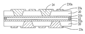
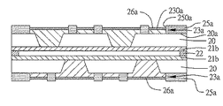
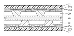
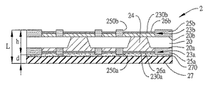
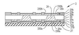
【解決手段】パッケージ基板2は、対向する2つの表面20a,20bを有するコア層20と、前記コア層20の2つの表面20a,20bに設けられた2つの回路層23a,23bと、前記コア層20に設けられた複数の導電ビア24と、前記コア層20の2つの表面20a,20b及び2つの回路層23a,23bに設けられた2つの絶縁保護層25a,25bと、前記コア層20のいずれか一方の表面20aの絶縁保護層25aに結合された搭載部材27とを備える。前記パッケージ基板2の一方の側に搭載部材27が結合されることにより、運送時又はパッケージング時に厚さが薄すぎることによる破損が回避される。
【選択図】 図2I
Description
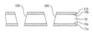
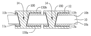
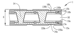
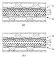
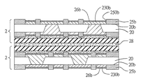
10、20 コア層
10a、20a 第1の表面
10b、20b 第2の表面
100、200 貫通孔
11a、21a 第1の金属層
11b、21b 第2の金属層
12 導電層
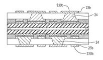
13a、23a 第1の回路層
13b、23b 第2の回路層
130a、230a 第1の電気接触パッド
130b、230b 第2の電気接触パッド
14、24 導電ビア
15a、25a 第1の絶縁保護層
15b、25b 第2の絶縁保護層
150a、250a 第1の開口
150b、250b 第2の開口
16a、26a 第1の表面処理層
16b、26b 第2の表面処理層
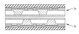
2a 基板本体
22 接着部材
27 搭載部材
270 接着層
28 結合部材
L、d、S 厚さ
h 残りの厚さ
Claims (2)
- 対向する第1の表面及び第2の表面を有するコア層と、
前記コア層の前記第1の表面に設けられ、第1の電気接触パッドを有する第1の回路層と、
前記コア層の前記第2の表面に設けられ、第2の電気接触パッドを有する第2の回路層と、
前記コア層に設けられ、前記第1及び第2の回路層に電気的に接続される導電ビアと、
前記コア層の前記第1の表面及び前記第1の回路層に設けられ、前記第1の電気接触パッドが露出される第1の絶縁保護層と、
前記第1の電気接触パッドの露出表面に形成される第1の表面処理層と、
前記コア層の前記第2の表面及び前記第2の回路層に設けられ、前記第2の電気接触パッドが露出される第2の絶縁保護層と、
前記第2の電気接触パッドの露出表面に形成される第2の表面処理層と、
前記第1の絶縁保護層に接着層により結合される搭載部材と、
を備えることを特徴とするパッケージ基板。 - 前記接着層の材質は、スーパーグルー又は離型剤であることを特徴とする請求項1に記載のパッケージ基板。
Priority Applications (1)
| Application Number | Priority Date | Filing Date | Title |
|---|---|---|---|
| JP2014053501A JP6000297B2 (ja) | 2014-03-17 | 2014-03-17 | パッケージ基板 |
Applications Claiming Priority (1)
| Application Number | Priority Date | Filing Date | Title |
|---|---|---|---|
| JP2014053501A JP6000297B2 (ja) | 2014-03-17 | 2014-03-17 | パッケージ基板 |
Related Parent Applications (1)
| Application Number | Title | Priority Date | Filing Date |
|---|---|---|---|
| JP2011276005A Division JP5536748B2 (ja) | 2011-12-16 | 2011-12-16 | パッケージ基板の製造方法 |
Publications (3)
| Publication Number | Publication Date |
|---|---|
| JP2014123772A true JP2014123772A (ja) | 2014-07-03 |
| JP2014123772A5 JP2014123772A5 (ja) | 2014-12-04 |
| JP6000297B2 JP6000297B2 (ja) | 2016-09-28 |
Family
ID=51403966
Family Applications (1)
| Application Number | Title | Priority Date | Filing Date |
|---|---|---|---|
| JP2014053501A Expired - Fee Related JP6000297B2 (ja) | 2014-03-17 | 2014-03-17 | パッケージ基板 |
Country Status (1)
| Country | Link |
|---|---|
| JP (1) | JP6000297B2 (ja) |
Citations (6)
| Publication number | Priority date | Publication date | Assignee | Title |
|---|---|---|---|---|
| JP2003324276A (ja) * | 2002-04-30 | 2003-11-14 | Ngk Spark Plug Co Ltd | 配線基板の製造方法 |
| JP2004140254A (ja) * | 2002-10-18 | 2004-05-13 | Toray Ind Inc | 多層回路基板用部材および多層回路基板の製造方法 |
| JP2009212140A (ja) * | 2008-02-29 | 2009-09-17 | Shinko Electric Ind Co Ltd | 配線基板の製造方法及び半導体パッケージの製造方法 |
| JP2010239126A (ja) * | 2009-03-09 | 2010-10-21 | Shinko Electric Ind Co Ltd | 半導体装置および半導体装置の製造方法 |
| JP2011009686A (ja) * | 2009-06-23 | 2011-01-13 | Kinko Denshi Kofun Yugenkoshi | パッケージ基板及びその製造方法、並びにその基材 |
| JP2011119722A (ja) * | 2009-11-09 | 2011-06-16 | Hitachi Chem Co Ltd | 多層配線基板及びその製造方法 |
-
2014
- 2014-03-17 JP JP2014053501A patent/JP6000297B2/ja not_active Expired - Fee Related
Patent Citations (6)
| Publication number | Priority date | Publication date | Assignee | Title |
|---|---|---|---|---|
| JP2003324276A (ja) * | 2002-04-30 | 2003-11-14 | Ngk Spark Plug Co Ltd | 配線基板の製造方法 |
| JP2004140254A (ja) * | 2002-10-18 | 2004-05-13 | Toray Ind Inc | 多層回路基板用部材および多層回路基板の製造方法 |
| JP2009212140A (ja) * | 2008-02-29 | 2009-09-17 | Shinko Electric Ind Co Ltd | 配線基板の製造方法及び半導体パッケージの製造方法 |
| JP2010239126A (ja) * | 2009-03-09 | 2010-10-21 | Shinko Electric Ind Co Ltd | 半導体装置および半導体装置の製造方法 |
| JP2011009686A (ja) * | 2009-06-23 | 2011-01-13 | Kinko Denshi Kofun Yugenkoshi | パッケージ基板及びその製造方法、並びにその基材 |
| JP2011119722A (ja) * | 2009-11-09 | 2011-06-16 | Hitachi Chem Co Ltd | 多層配線基板及びその製造方法 |
Also Published As
| Publication number | Publication date |
|---|---|
| JP6000297B2 (ja) | 2016-09-28 |
Similar Documents
| Publication | Publication Date | Title |
|---|---|---|
| TWI493671B (zh) | 具有支撐體的封裝基板及其製法、具有支撐體的封裝結構及其製法 | |
| US20120049366A1 (en) | Package structure having through-silicon-via (tsv) chip embedded therein and fabrication method thereof | |
| TW201505507A (zh) | 封裝基板、封裝結構以及封裝基板的製作方法 | |
| US20130075928A1 (en) | Integrated circuit and method of making | |
| TW200822830A (en) | Circuit board structure and fabrication method thereof | |
| CN118553709A (zh) | 封装基板及其制法 | |
| CN104795356A (zh) | 半导体封装件及其制法 | |
| US8828796B1 (en) | Semiconductor package and method of manufacturing the same | |
| US8628636B2 (en) | Method of manufacturing a package substrate | |
| KR101043328B1 (ko) | 전자소자 내장형 인쇄회로기판 및 그 제조방법 | |
| JP5346388B2 (ja) | パッケージ基板の製造方法 | |
| CN118553621B (zh) | 封装基板的制法 | |
| CN103208429B (zh) | 封装基板的制法 | |
| CN103066049B (zh) | 封装基板及其制法 | |
| JP6000297B2 (ja) | パッケージ基板 | |
| JP5536748B2 (ja) | パッケージ基板の製造方法 | |
| CN104103602A (zh) | 半导体封装件及其制法 | |
| US9084341B2 (en) | Fabrication method of packaging substrate | |
| KR101378311B1 (ko) | 패키징 기판 및 그 제조 방법 | |
| TWI520276B (zh) | 封裝基板及其製法 | |
| TWI558286B (zh) | 封裝結構及其製法 | |
| TW201601224A (zh) | 封裝基板結構及其製法 | |
| JP5934057B2 (ja) | プリント回路基板 | |
| KR101299140B1 (ko) | 패키지 기판 제조 방법 | |
| KR102117481B1 (ko) | 인쇄회로기판 및 그 제조방법 |
Legal Events
| Date | Code | Title | Description |
|---|---|---|---|
| A521 | Written amendment |
Free format text: JAPANESE INTERMEDIATE CODE: A523 Effective date: 20141020 |
|
| A621 | Written request for application examination |
Free format text: JAPANESE INTERMEDIATE CODE: A621 Effective date: 20141020 |
|
| A977 | Report on retrieval |
Free format text: JAPANESE INTERMEDIATE CODE: A971007 Effective date: 20150710 |
|
| A131 | Notification of reasons for refusal |
Free format text: JAPANESE INTERMEDIATE CODE: A131 Effective date: 20150721 |
|
| RD02 | Notification of acceptance of power of attorney |
Free format text: JAPANESE INTERMEDIATE CODE: A7422 Effective date: 20150914 |
|
| A521 | Written amendment |
Free format text: JAPANESE INTERMEDIATE CODE: A821 Effective date: 20150914 |
|
| RD04 | Notification of resignation of power of attorney |
Free format text: JAPANESE INTERMEDIATE CODE: A7424 Effective date: 20151009 |
|
| A521 | Written amendment |
Free format text: JAPANESE INTERMEDIATE CODE: A523 Effective date: 20151015 |
|
| A131 | Notification of reasons for refusal |
Free format text: JAPANESE INTERMEDIATE CODE: A131 Effective date: 20160419 |
|
| A521 | Written amendment |
Free format text: JAPANESE INTERMEDIATE CODE: A523 Effective date: 20160707 |
|
| TRDD | Decision of grant or rejection written | ||
| A01 | Written decision to grant a patent or to grant a registration (utility model) |
Free format text: JAPANESE INTERMEDIATE CODE: A01 Effective date: 20160809 |
|
| A61 | First payment of annual fees (during grant procedure) |
Free format text: JAPANESE INTERMEDIATE CODE: A61 Effective date: 20160830 |
|
| R150 | Certificate of patent or registration of utility model |
Ref document number: 6000297 Country of ref document: JP Free format text: JAPANESE INTERMEDIATE CODE: R150 |
|
| R250 | Receipt of annual fees |
Free format text: JAPANESE INTERMEDIATE CODE: R250 |
|
| LAPS | Cancellation because of no payment of annual fees |