JP2014116604A - 発光素子 - Google Patents
発光素子 Download PDFInfo
- Publication number
- JP2014116604A JP2014116604A JP2013251766A JP2013251766A JP2014116604A JP 2014116604 A JP2014116604 A JP 2014116604A JP 2013251766 A JP2013251766 A JP 2013251766A JP 2013251766 A JP2013251766 A JP 2013251766A JP 2014116604 A JP2014116604 A JP 2014116604A
- Authority
- JP
- Japan
- Prior art keywords
- light emitting
- layer
- electrode
- disposed
- current blocking
- Prior art date
- Legal status (The legal status is an assumption and is not a legal conclusion. Google has not performed a legal analysis and makes no representation as to the accuracy of the status listed.)
- Pending
Links
Images


Classifications
-
- H—ELECTRICITY
- H01—ELECTRIC ELEMENTS
- H01L—SEMICONDUCTOR DEVICES NOT COVERED BY CLASS H10
- H01L27/00—Devices consisting of a plurality of semiconductor or other solid-state components formed in or on a common substrate
- H01L27/15—Devices consisting of a plurality of semiconductor or other solid-state components formed in or on a common substrate including semiconductor components with at least one potential-jump barrier or surface barrier specially adapted for light emission
- H01L27/153—Devices consisting of a plurality of semiconductor or other solid-state components formed in or on a common substrate including semiconductor components with at least one potential-jump barrier or surface barrier specially adapted for light emission in a repetitive configuration, e.g. LED bars
- H01L27/156—Devices consisting of a plurality of semiconductor or other solid-state components formed in or on a common substrate including semiconductor components with at least one potential-jump barrier or surface barrier specially adapted for light emission in a repetitive configuration, e.g. LED bars two-dimensional arrays
-
- H—ELECTRICITY
- H01—ELECTRIC ELEMENTS
- H01L—SEMICONDUCTOR DEVICES NOT COVERED BY CLASS H10
- H01L27/00—Devices consisting of a plurality of semiconductor or other solid-state components formed in or on a common substrate
- H01L27/15—Devices consisting of a plurality of semiconductor or other solid-state components formed in or on a common substrate including semiconductor components with at least one potential-jump barrier or surface barrier specially adapted for light emission
-
- H—ELECTRICITY
- H01—ELECTRIC ELEMENTS
- H01L—SEMICONDUCTOR DEVICES NOT COVERED BY CLASS H10
- H01L33/00—Semiconductor devices with at least one potential-jump barrier or surface barrier specially adapted for light emission; Processes or apparatus specially adapted for the manufacture or treatment thereof or of parts thereof; Details thereof
- H01L33/02—Semiconductor devices with at least one potential-jump barrier or surface barrier specially adapted for light emission; Processes or apparatus specially adapted for the manufacture or treatment thereof or of parts thereof; Details thereof characterised by the semiconductor bodies
- H01L33/10—Semiconductor devices with at least one potential-jump barrier or surface barrier specially adapted for light emission; Processes or apparatus specially adapted for the manufacture or treatment thereof or of parts thereof; Details thereof characterised by the semiconductor bodies with a light reflecting structure, e.g. semiconductor Bragg reflector
-
- H—ELECTRICITY
- H01—ELECTRIC ELEMENTS
- H01L—SEMICONDUCTOR DEVICES NOT COVERED BY CLASS H10
- H01L33/00—Semiconductor devices with at least one potential-jump barrier or surface barrier specially adapted for light emission; Processes or apparatus specially adapted for the manufacture or treatment thereof or of parts thereof; Details thereof
- H01L33/02—Semiconductor devices with at least one potential-jump barrier or surface barrier specially adapted for light emission; Processes or apparatus specially adapted for the manufacture or treatment thereof or of parts thereof; Details thereof characterised by the semiconductor bodies
- H01L33/14—Semiconductor devices with at least one potential-jump barrier or surface barrier specially adapted for light emission; Processes or apparatus specially adapted for the manufacture or treatment thereof or of parts thereof; Details thereof characterised by the semiconductor bodies with a carrier transport control structure, e.g. highly-doped semiconductor layer or current-blocking structure
- H01L33/145—Semiconductor devices with at least one potential-jump barrier or surface barrier specially adapted for light emission; Processes or apparatus specially adapted for the manufacture or treatment thereof or of parts thereof; Details thereof characterised by the semiconductor bodies with a carrier transport control structure, e.g. highly-doped semiconductor layer or current-blocking structure with a current-blocking structure
-
- H—ELECTRICITY
- H01—ELECTRIC ELEMENTS
- H01L—SEMICONDUCTOR DEVICES NOT COVERED BY CLASS H10
- H01L33/00—Semiconductor devices with at least one potential-jump barrier or surface barrier specially adapted for light emission; Processes or apparatus specially adapted for the manufacture or treatment thereof or of parts thereof; Details thereof
- H01L33/36—Semiconductor devices with at least one potential-jump barrier or surface barrier specially adapted for light emission; Processes or apparatus specially adapted for the manufacture or treatment thereof or of parts thereof; Details thereof characterised by the electrodes
- H01L33/40—Materials therefor
- H01L33/42—Transparent materials
-
- H—ELECTRICITY
- H01—ELECTRIC ELEMENTS
- H01L—SEMICONDUCTOR DEVICES NOT COVERED BY CLASS H10
- H01L33/00—Semiconductor devices with at least one potential-jump barrier or surface barrier specially adapted for light emission; Processes or apparatus specially adapted for the manufacture or treatment thereof or of parts thereof; Details thereof
- H01L33/48—Semiconductor devices with at least one potential-jump barrier or surface barrier specially adapted for light emission; Processes or apparatus specially adapted for the manufacture or treatment thereof or of parts thereof; Details thereof characterised by the semiconductor body packages
- H01L33/62—Arrangements for conducting electric current to or from the semiconductor body, e.g. lead-frames, wire-bonds or solder balls
-
- H—ELECTRICITY
- H01—ELECTRIC ELEMENTS
- H01L—SEMICONDUCTOR DEVICES NOT COVERED BY CLASS H10
- H01L2924/00—Indexing scheme for arrangements or methods for connecting or disconnecting semiconductor or solid-state bodies as covered by H01L24/00
- H01L2924/0001—Technical content checked by a classifier
- H01L2924/0002—Not covered by any one of groups H01L24/00, H01L24/00 and H01L2224/00
-
- H—ELECTRICITY
- H01—ELECTRIC ELEMENTS
- H01L—SEMICONDUCTOR DEVICES NOT COVERED BY CLASS H10
- H01L33/00—Semiconductor devices with at least one potential-jump barrier or surface barrier specially adapted for light emission; Processes or apparatus specially adapted for the manufacture or treatment thereof or of parts thereof; Details thereof
- H01L33/36—Semiconductor devices with at least one potential-jump barrier or surface barrier specially adapted for light emission; Processes or apparatus specially adapted for the manufacture or treatment thereof or of parts thereof; Details thereof characterised by the electrodes
- H01L33/38—Semiconductor devices with at least one potential-jump barrier or surface barrier specially adapted for light emission; Processes or apparatus specially adapted for the manufacture or treatment thereof or of parts thereof; Details thereof characterised by the electrodes with a particular shape
- H01L33/385—Semiconductor devices with at least one potential-jump barrier or surface barrier specially adapted for light emission; Processes or apparatus specially adapted for the manufacture or treatment thereof or of parts thereof; Details thereof characterised by the electrodes with a particular shape the electrode extending at least partially onto a side surface of the semiconductor body
Abstract
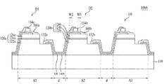
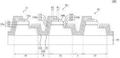
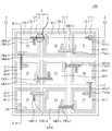
【解決手段】発光素子100Aは、基板110と基板上に互いに離隔して配列され、下部及び上部半導体層122a、126aと活性層124aを有する発光構造物120a、上部電極134a及び下部電極132aを含む複数の発光セルD1と隣接する複数の発光セルのうち一方の第1発光セルの下部電極と、他方の第2発光セルの上部電極とを電気的に接続する導電型相互連結層150と第2発光セルの上部電極と上部半導体層との間から、隣接する複数の発光セルと導電型相互連結層との間に延びて配置された電流遮断層140Aとを含み、複数の発光セルのそれぞれは、第2発光セルの上部電極と電流遮断層との間から、第2発光セルの上部半導体層の上に延びて配置されて、第2発光セルの上部電極と第2発光セルの上部半導体層とを電気的に接続する伝導層160aをさらに含む。
【選択図】図2
Description
Claims (10)
- 基板と、
前記基板上に水平方向に互いに離隔して配列され、それぞれは、互いに異なる導電型の下部及び上部半導体層、前記下部及び上部半導体層の間に配置された活性層を有する発光構造物と、前記上部半導体層上に配置された上部電極と、前記下部半導体層上に配置された下部電極とを含む複数の発光セルと、
隣接する複数の発光セルのうち一方の第1発光セルの下部電極と、前記隣接する複数の発光セルのうち他方の第2発光セルの上部電極とを電気的に接続する導電型相互連結層と、
前記第2発光セルの上部電極と上部半導体層との間から前記隣接する複数の発光セルと前記導電型相互連結層との間に延びて配置された電流遮断層とを含み、
前記複数の発光セルのそれぞれは、
前記第2発光セルの上部電極と前記電流遮断層との間から前記第2発光セルの上部半導体層の上に延びて配置されて、前記第2発光セルの上部電極と第2発光セルの上部半導体層とを電気的に接続する伝導層をさらに含む、発光素子。 - 前記電流遮断層は、
前記第1発光セルの下部半導体層と前記導電型相互連結層との間、前記基板と前記導電型相互連結層との間、及び前記第2発光セルの発光構造物と前記導電型相互連結層との間に配置される、請求項1に記載の発光素子。 - 前記第2発光セルの上部電極は、前記第2発光セルの前記上部半導体層と対向する下部面を有し、
前記第2発光セルの上部電極と上部半導体層との間に配置される前記電流遮断層は、前記上部電極と対向する上部面を有し、
前記電流遮断層の上部面の面積は、前記上部電極の下部面全体の面積以上である、請求項1又は2に記載の発光素子。 - 前記第2発光セルの上部電極と前記第1発光セルの下部電極と前記導電型相互連結層とは一体型層である、請求項1ないし3のいずれかに記載の発光素子。
- 前記一体型層は、前記第2発光セルの前記上部半導体層と対向する下部面を有し、
前記一体型層と前記第2発光セルの上部半導体層との間に配置される前記電流遮断層は、前記一体型層と対向する上部面を有し、
前記電流遮断層の上部面の面積は、前記一体型層の下部面全体の面積以上である、請求項4に記載の発光素子。 - 前記上部半導体層の上部に配置された前記伝導層の面積は、前記上部半導体層の上部面の面積以下である、請求項1ないし5のいずれかに記載の発光素子。
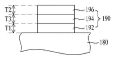
- 前記電流遮断層は、分散ブラッグ反射層である、請求項1に記載の発光素子。
- 前記分散ブラッグ反射層は、屈折率の互いに異なる第1及び第2層が交互に少なくとも1回以上積層された絶縁物質を含む、請求項7に記載の発光素子。
- 前記上部電極は、
互いに重なる第1接着層及び第1ボンディング層を含み、前記第1接着層と前記第1ボンディング層との間に反射層が介在していない、請求項1ないし8のいずれかに記載の発光素子。 - 前記下部電極は、
互いに重なる第2接着層及び第2ボンディング層を含み、前記第2接着層と前記第2ボンディング層との間に反射層が介在していない、請求項1ないし9のいずれかに記載の発光素子。
Applications Claiming Priority (2)
| Application Number | Priority Date | Filing Date | Title |
|---|---|---|---|
| KR1020120141503A KR20140073351A (ko) | 2012-12-06 | 2012-12-06 | 발광 소자 |
| KR10-2012-0141503 | 2012-12-06 |
Publications (2)
| Publication Number | Publication Date |
|---|---|
| JP2014116604A true JP2014116604A (ja) | 2014-06-26 |
| JP2014116604A5 JP2014116604A5 (ja) | 2017-01-12 |
Family
ID=49683623
Family Applications (1)
| Application Number | Title | Priority Date | Filing Date |
|---|---|---|---|
| JP2013251766A Pending JP2014116604A (ja) | 2012-12-06 | 2013-12-05 | 発光素子 |
Country Status (5)
| Country | Link |
|---|---|
| US (2) | US9337236B2 (ja) |
| EP (1) | EP2741338B1 (ja) |
| JP (1) | JP2014116604A (ja) |
| KR (1) | KR20140073351A (ja) |
| CN (1) | CN103855180B (ja) |
Cited By (7)
| Publication number | Priority date | Publication date | Assignee | Title |
|---|---|---|---|---|
| JP2016012707A (ja) * | 2014-06-30 | 2016-01-21 | 晶元光電股▲ふん▼有限公司 | 光電部品及びその製造方法 |
| JP2017059752A (ja) * | 2015-09-18 | 2017-03-23 | 豊田合成株式会社 | 発光装置とその製造方法 |
| JP2019145843A (ja) * | 2019-05-14 | 2019-08-29 | 晶元光電股▲ふん▼有限公司Epistar Corporation | 光電部品 |
| US10903394B2 (en) | 2018-02-19 | 2021-01-26 | Nichia Corporation | Light emitting element |
| JP2021082837A (ja) * | 2021-02-24 | 2021-05-27 | 晶元光電股▲ふん▼有限公司Epistar Corporation | 光電部品 |
| US11355550B2 (en) | 2014-05-19 | 2022-06-07 | Epistar Corporation | Optoelectronic device having conductor arrangement structures non-overlapped with heat dissipation pads |
| WO2023068264A1 (ja) * | 2021-10-18 | 2023-04-27 | 浜松ホトニクス株式会社 | 光半導体素子 |
Families Citing this family (41)
| Publication number | Priority date | Publication date | Assignee | Title |
|---|---|---|---|---|
| CN103840054A (zh) * | 2012-11-20 | 2014-06-04 | 展晶科技(深圳)有限公司 | 发光二极管芯片 |
| KR20140073351A (ko) * | 2012-12-06 | 2014-06-16 | 엘지이노텍 주식회사 | 발광 소자 |
| US9356212B2 (en) | 2012-12-21 | 2016-05-31 | Seoul Viosys Co., Ltd. | Light emitting diode and method of fabricating the same |
| WO2014098510A1 (en) * | 2012-12-21 | 2014-06-26 | Seoul Viosys Co., Ltd. | Light emitting diode and method of fabricating the same |
| CN103915463B (zh) * | 2013-01-09 | 2016-12-28 | 新世纪光电股份有限公司 | 发光装置 |
| KR20150101783A (ko) * | 2014-02-27 | 2015-09-04 | 서울바이오시스 주식회사 | 발광 다이오드 및 그 제조 방법 |
| KR102197082B1 (ko) * | 2014-06-16 | 2020-12-31 | 엘지이노텍 주식회사 | 발광 소자 및 이를 포함하는 발광소자 패키지 |
| FR3023061B1 (fr) * | 2014-06-27 | 2017-12-15 | Commissariat Energie Atomique | Diode de structure mesa a surface de contact sensiblement plane |
| KR102052040B1 (ko) * | 2014-06-30 | 2019-12-04 | 에피스타 코포레이션 | 광전소자와 그 제조방법 |
| CN104218133B (zh) * | 2014-08-26 | 2017-04-26 | 华灿光电股份有限公司 | 一种发光二极管芯片及其制造方法 |
| CN104362236B (zh) * | 2014-11-11 | 2017-03-08 | 杭州士兰明芯科技有限公司 | 一种led结构及其制作方法 |
| TWI620349B (zh) * | 2015-01-05 | 2018-04-01 | 隆達電子股份有限公司 | 覆晶式發光二極體晶片 |
| CN110690250A (zh) * | 2015-02-13 | 2020-01-14 | 首尔伟傲世有限公司 | 发光元件和发光二极管 |
| TWI723897B (zh) * | 2015-04-22 | 2021-04-01 | 新世紀光電股份有限公司 | 發光元件之製造方法 |
| US10147849B2 (en) * | 2015-05-05 | 2018-12-04 | Xiangneng Hualei Optoelectronic Co., Ltd | Manufacturing method of flip-chip structure of group III semiconductor light emitting device |
| US9705035B1 (en) | 2015-12-30 | 2017-07-11 | Epistar Corporation | Light emitting device |
| DE102017205639A1 (de) * | 2016-04-18 | 2017-10-19 | Seoul Viosys Co., Ltd | Lumineszenzdiode mit hoher Effizienz |
| KR102641965B1 (ko) * | 2016-11-10 | 2024-02-29 | 서울바이오시스 주식회사 | 고효율 발광 다이오드 |
| CN105762246B (zh) * | 2016-04-25 | 2017-11-28 | 厦门乾照光电股份有限公司 | 一种垂直结构发光二极管及其制作方法 |
| KR102510006B1 (ko) * | 2016-05-24 | 2023-03-14 | 엘지이노텍 주식회사 | 반도체 소자 |
| KR20180007025A (ko) * | 2016-07-11 | 2018-01-22 | 삼성디스플레이 주식회사 | 초소형 발광 소자를 포함하는 픽셀 구조체, 표시장치 및 그 제조방법 |
| CN106711306A (zh) * | 2016-12-20 | 2017-05-24 | 合肥彩虹蓝光科技有限公司 | 一种高压led芯片制备方法 |
| WO2018137139A1 (en) * | 2017-01-24 | 2018-08-02 | Goertek. Inc | Micro-led device, display apparatus and method for manufacturing a micro-led device |
| US10043941B1 (en) | 2017-01-31 | 2018-08-07 | International Business Machines Corporation | Light emitting diode having improved quantum efficiency at low injection current |
| FR3062953A1 (fr) * | 2017-02-15 | 2018-08-17 | Commissariat A L'energie Atomique Et Aux Energies Alternatives | Dispositif comportant une pluralite de diodes |
| DE102017104135A1 (de) | 2017-02-28 | 2018-08-30 | Osram Opto Semiconductors Gmbh | Optoelektronisches Bauelement und Verfahren zur Herstellung eines optoelektronischen Bauelements |
| KR20180106720A (ko) * | 2017-03-21 | 2018-10-01 | 서울바이오시스 주식회사 | 분포 브래그 반사기 적층체를 구비하는 발광 다이오드 |
| CN106941108B (zh) * | 2017-05-23 | 2019-09-17 | 深圳市华星光电技术有限公司 | 微发光二极管显示面板及其制作方法 |
| CN108110107A (zh) * | 2017-12-18 | 2018-06-01 | 湘能华磊光电股份有限公司 | 一种led芯片的制作方法 |
| KR20190094283A (ko) | 2018-02-03 | 2019-08-13 | 김승훈 | 기억 상기 다기능 테이블 |
| JP2019149480A (ja) * | 2018-02-27 | 2019-09-05 | 豊田合成株式会社 | 半導体素子、発光装置、および発光装置の製造方法 |
| CN108447955B (zh) | 2018-03-16 | 2019-07-23 | 厦门市三安光电科技有限公司 | 发光二极管芯片结构及其制作方法 |
| CN208385406U (zh) * | 2018-05-25 | 2019-01-15 | 深圳市瑞丰光电子股份有限公司 | 一种led模组 |
| US11282984B2 (en) * | 2018-10-05 | 2022-03-22 | Seoul Viosys Co., Ltd. | Light emitting device |
| CN109891610A (zh) * | 2018-10-11 | 2019-06-14 | 厦门市三安光电科技有限公司 | 一种发光二极管元件及其制作方法 |
| US11515456B2 (en) * | 2019-02-21 | 2022-11-29 | Innolux Corporation | LED with light adjusting layer extending past the LED |
| KR102649029B1 (ko) * | 2019-04-10 | 2024-03-20 | 삼성전자주식회사 | Led 소자, led 소자의 제조 방법 및 led 소자를 포함하는 디스플레이 장치 |
| CN110767670B (zh) * | 2019-10-31 | 2022-11-15 | 成都辰显光电有限公司 | 显示面板、显示装置和显示面板的制作方法 |
| CN113036014B (zh) * | 2019-12-25 | 2022-07-05 | 深圳第三代半导体研究院 | 一种垂直集成单元发光二极管 |
| US11901491B2 (en) * | 2020-10-29 | 2024-02-13 | Lumileds Llc | Light emitting diode devices |
| WO2024053994A1 (ko) * | 2022-09-06 | 2024-03-14 | 서울반도체 주식회사 | 발광장치 |
Citations (10)
| Publication number | Priority date | Publication date | Assignee | Title |
|---|---|---|---|---|
| JP2000101136A (ja) * | 1998-09-25 | 2000-04-07 | Toshiba Corp | 半導体発光装置及び半導体発光装置の駆動方法 |
| JP2002026384A (ja) * | 2000-07-05 | 2002-01-25 | Nichia Chem Ind Ltd | 集積型窒化物半導体発光素子 |
| US20060169993A1 (en) * | 2005-02-03 | 2006-08-03 | Zhaoyang Fan | Micro-LED based high voltage AC/DC indicator lamp |
| JP2009071220A (ja) * | 2007-09-18 | 2009-04-02 | Toyoda Gosei Co Ltd | Iii族窒化物系化合物半導体発光素子 |
| JP2009302314A (ja) * | 2008-06-13 | 2009-12-24 | Rohm Co Ltd | GaN系半導体装置 |
| JP2010056195A (ja) * | 2008-08-27 | 2010-03-11 | Nichia Corp | 半導体発光素子 |
| US20100237371A1 (en) * | 2007-10-04 | 2010-09-23 | Bong Cheol Kang | Light emitting device and method for fabricating the same |
| JP2012028749A (ja) * | 2010-07-22 | 2012-02-09 | Seoul Opto Devices Co Ltd | 発光ダイオード |
| JP2012507134A (ja) * | 2008-09-11 | 2012-03-22 | ブリッジラックス・インク | 直列接続されたセグメント化led |
| JP2012519377A (ja) * | 2009-02-26 | 2012-08-23 | ブリッジラックス インコーポレイテッド | 個々のセグメントledの光出力における製造工程でのばらつきを補償するセグメントledを用いた光源 |
Family Cites Families (10)
| Publication number | Priority date | Publication date | Assignee | Title |
|---|---|---|---|---|
| DE60043536D1 (de) * | 1999-03-04 | 2010-01-28 | Nichia Corp | Nitridhalbleiterlaserelement |
| US6630689B2 (en) | 2001-05-09 | 2003-10-07 | Lumileds Lighting, U.S. Llc | Semiconductor LED flip-chip with high reflectivity dielectric coating on the mesa |
| KR100640496B1 (ko) * | 2005-11-23 | 2006-11-01 | 삼성전기주식회사 | 수직구조 질화갈륨계 발광다이오드 소자 |
| CN101485000B (zh) | 2006-06-23 | 2012-01-11 | Lg电子株式会社 | 具有垂直拓扑的发光二极管及其制造方法 |
| US8536584B2 (en) | 2007-11-14 | 2013-09-17 | Cree, Inc. | High voltage wire bond free LEDS |
| JP5123269B2 (ja) | 2008-09-30 | 2013-01-23 | ソウル オプト デバイス カンパニー リミテッド | 発光素子及びその製造方法 |
| KR20100076083A (ko) * | 2008-12-17 | 2010-07-06 | 서울반도체 주식회사 | 복수개의 발광셀들을 갖는 발광 다이오드 및 그것을 제조하는 방법 |
| KR101533817B1 (ko) | 2008-12-31 | 2015-07-09 | 서울바이오시스 주식회사 | 복수개의 비극성 발광셀들을 갖는 발광 소자 및 그것을 제조하는 방법 |
| CN102201426B (zh) * | 2010-03-23 | 2016-05-04 | 展晶科技(深圳)有限公司 | 发光二极管及其制作方法 |
| KR20140073351A (ko) * | 2012-12-06 | 2014-06-16 | 엘지이노텍 주식회사 | 발광 소자 |
-
2012
- 2012-12-06 KR KR1020120141503A patent/KR20140073351A/ko not_active Application Discontinuation
-
2013
- 2013-12-04 EP EP13195745.8A patent/EP2741338B1/en active Active
- 2013-12-04 US US14/096,138 patent/US9337236B2/en active Active
- 2013-12-05 JP JP2013251766A patent/JP2014116604A/ja active Pending
- 2013-12-05 CN CN201310651693.6A patent/CN103855180B/zh active Active
-
2016
- 2016-04-07 US US15/092,682 patent/US9735199B2/en active Active
Patent Citations (10)
| Publication number | Priority date | Publication date | Assignee | Title |
|---|---|---|---|---|
| JP2000101136A (ja) * | 1998-09-25 | 2000-04-07 | Toshiba Corp | 半導体発光装置及び半導体発光装置の駆動方法 |
| JP2002026384A (ja) * | 2000-07-05 | 2002-01-25 | Nichia Chem Ind Ltd | 集積型窒化物半導体発光素子 |
| US20060169993A1 (en) * | 2005-02-03 | 2006-08-03 | Zhaoyang Fan | Micro-LED based high voltage AC/DC indicator lamp |
| JP2009071220A (ja) * | 2007-09-18 | 2009-04-02 | Toyoda Gosei Co Ltd | Iii族窒化物系化合物半導体発光素子 |
| US20100237371A1 (en) * | 2007-10-04 | 2010-09-23 | Bong Cheol Kang | Light emitting device and method for fabricating the same |
| JP2009302314A (ja) * | 2008-06-13 | 2009-12-24 | Rohm Co Ltd | GaN系半導体装置 |
| JP2010056195A (ja) * | 2008-08-27 | 2010-03-11 | Nichia Corp | 半導体発光素子 |
| JP2012507134A (ja) * | 2008-09-11 | 2012-03-22 | ブリッジラックス・インク | 直列接続されたセグメント化led |
| JP2012519377A (ja) * | 2009-02-26 | 2012-08-23 | ブリッジラックス インコーポレイテッド | 個々のセグメントledの光出力における製造工程でのばらつきを補償するセグメントledを用いた光源 |
| JP2012028749A (ja) * | 2010-07-22 | 2012-02-09 | Seoul Opto Devices Co Ltd | 発光ダイオード |
Cited By (10)
| Publication number | Priority date | Publication date | Assignee | Title |
|---|---|---|---|---|
| US11355550B2 (en) | 2014-05-19 | 2022-06-07 | Epistar Corporation | Optoelectronic device having conductor arrangement structures non-overlapped with heat dissipation pads |
| US11705480B2 (en) | 2014-05-19 | 2023-07-18 | Epistar Corporation | Optoelectronic device with electrodes forming an outer boundary beyond an outer boundary of an epitaxial stack |
| JP2016012707A (ja) * | 2014-06-30 | 2016-01-21 | 晶元光電股▲ふん▼有限公司 | 光電部品及びその製造方法 |
| JP2017059752A (ja) * | 2015-09-18 | 2017-03-23 | 豊田合成株式会社 | 発光装置とその製造方法 |
| US10903394B2 (en) | 2018-02-19 | 2021-01-26 | Nichia Corporation | Light emitting element |
| US11715814B2 (en) | 2018-02-19 | 2023-08-01 | Nichia Corporation | Light emitting element including first and second semiconductor layered bodies having defined relative lateral surface angles |
| JP2019145843A (ja) * | 2019-05-14 | 2019-08-29 | 晶元光電股▲ふん▼有限公司Epistar Corporation | 光電部品 |
| JP2021082837A (ja) * | 2021-02-24 | 2021-05-27 | 晶元光電股▲ふん▼有限公司Epistar Corporation | 光電部品 |
| JP7223046B2 (ja) | 2021-02-24 | 2023-02-15 | 晶元光電股▲ふん▼有限公司 | 光電部品 |
| WO2023068264A1 (ja) * | 2021-10-18 | 2023-04-27 | 浜松ホトニクス株式会社 | 光半導体素子 |
Also Published As
| Publication number | Publication date |
|---|---|
| US9337236B2 (en) | 2016-05-10 |
| KR20140073351A (ko) | 2014-06-16 |
| US20160225816A1 (en) | 2016-08-04 |
| CN103855180B (zh) | 2019-11-05 |
| US20140159071A1 (en) | 2014-06-12 |
| US9735199B2 (en) | 2017-08-15 |
| CN103855180A (zh) | 2014-06-11 |
| EP2741338A1 (en) | 2014-06-11 |
| EP2741338B1 (en) | 2020-05-20 |
Similar Documents
| Publication | Publication Date | Title |
|---|---|---|
| EP2741338B1 (en) | Electrode structure for light-emitting diode array | |
| KR102087933B1 (ko) | 발광 소자 및 이를 포함하는 발광 소자 어레이 | |
| KR101888604B1 (ko) | 발광 소자 및 발광 소자 패키지 | |
| JP6053453B2 (ja) | 発光素子 | |
| KR101871372B1 (ko) | 발광 소자 | |
| US9812626B2 (en) | Light emitting device | |
| US9837577B2 (en) | Light emitting device | |
| KR101712050B1 (ko) | 발광 소자 패키지 | |
| KR101830719B1 (ko) | 발광 소자 | |
| KR20140092037A (ko) | 발광 소자 패키지 |
Legal Events
| Date | Code | Title | Description |
|---|---|---|---|
| A521 | Request for written amendment filed |
Free format text: JAPANESE INTERMEDIATE CODE: A523 Effective date: 20161124 |
|
| A621 | Written request for application examination |
Free format text: JAPANESE INTERMEDIATE CODE: A621 Effective date: 20161124 |
|
| A977 | Report on retrieval |
Free format text: JAPANESE INTERMEDIATE CODE: A971007 Effective date: 20171031 |
|
| A131 | Notification of reasons for refusal |
Free format text: JAPANESE INTERMEDIATE CODE: A131 Effective date: 20171121 |
|
| A521 | Request for written amendment filed |
Free format text: JAPANESE INTERMEDIATE CODE: A523 Effective date: 20180220 |
|
| A131 | Notification of reasons for refusal |
Free format text: JAPANESE INTERMEDIATE CODE: A131 Effective date: 20180717 |
|
| A521 | Request for written amendment filed |
Free format text: JAPANESE INTERMEDIATE CODE: A523 Effective date: 20181016 |
|
| A02 | Decision of refusal |
Free format text: JAPANESE INTERMEDIATE CODE: A02 Effective date: 20190402 |